Cryogenic operation of silicon photonic modulators based on DC Kerr effect
Abstract
Reliable operation of photonic integrated circuits at cryogenic temperatures would enable new capabilities for emerging computing platforms, such as quantum technologies and low-power cryogenic computing. The silicon-on-insulator platform is a highly promising approach to developing large-scale photonic integrated circuits due to its exceptional manufacturability, CMOS compatibility and high component density. Fast, efficient and low-loss modulation at cryogenic temperatures in silicon, however, remains an outstanding challenge, particularly without the addition of exotic nonlinear optical materials. In this paper, we demonstrate DC-Kerr-effect-based modulation at a temperature of 5 K at GHz speeds, in a silicon photonic device fabricated exclusively within a CMOS process. This work opens up the path for the integration of DC Kerr modulators in large-scale photonic integrated circuits for emerging cryogenic classical and quantum computing applications.
I Introduction
Photonic integrated circuits (PICs) have emerged as a promising platform for a wide range of integrated optical computing and signal processing applications. PICs are a highly attractive candidate for quantum technologies due to the ease with which they can generate, manipulate and detect quantum states of light in a compact architecture Wang et al. (2020). These systems can now be accessed through commercial photonics foundries Hochberg and Baehr-Jones (2010), paving the way for a new paradigm in large-scale photonic quantum information processing Carolan et al. (2015); Wang et al. (2020) and quantum key distribution Sibson et al. (2017); Bunandar et al. (2018). The CMOS-compatibility and large refractive index contrast of the silicon-on-insulator platform makes it particularly well suited for large-scale quantum photonics Silverstone et al. (2016); Rudolph (2017) and optical data transmission.
However, integration of silicon photonics with key quantum componentry — including single photon emitters Kim et al. (2020); Elshaari et al. (2020), quantum memories Dibos et al. (2018) and single photon detectors Najafi et al. (2014); Shibata et al. (2019) — will likely require operation at cryogenic ( K) temperatures. Silicon photonics provides an efficient platform for electro-optic interconnects, which can reduce passive heat loading and provide a high-speed, low-loss solution to limitations on electrical connections in cryogenically-cooled circuits Youssefi et al. (2020). Low-power cryogenic systems for classical computing, such as superconducting optoelectronic circuits Shainline et al. (2018), must also be operated at K temperatures Holmes et al. (2013).
The major challenge in the operation of silicon quantum photonics at cryogenic temperatures is the absence of fast, low-loss, phase-only modulation technology, which is required for active multiplexing Gimeno-Segovia et al. (2017) and high-fidelity quantum gates Laing et al. (2010). To date, silicon photonic modulators typically rely on the plasma dispersion effect Reed et al. (2010); Timurdogan et al. (2014); Pérez-Galacho et al. (2015) or the (typically slow) thermo-optic effect Harris et al. (2014). At cryogenic temperatures, thermo-optic modulators suffer from a decrease in the thermo-optic coefficient of silicon by four orders of magnitude Komma et al. (2012). Plasma dispersion modulators can suffer from large carrier-induced losses and can be bandwidth-limited by low-temperature carrier freeze-out Gehl et al. (2017); Pires et al. (1990).
While silicon’s intrinsic third order nonlinearity makes it an excellent candidate for nonlinear processes such as four-wave mixing Faruque et al. (2018); Carolan et al. (2019), silicon’s crystal centro-symmetry precludes the existence of a native second-order nonlinearity. Thus, unlike non-centro-symmetric materials such as lithium niobate (LiNbO3) and gallium arsenide (GaAs), silicon cannot be a natural candidate for Pockels-effect-based electro-optic modulators. One approach is to integrate materials that possess a strong second-order nonlinearity such as LiNbO3 He et al. (2019) or barium titanate (BaTiO3) Eltes et al. (2019) into the silicon photonics platform. Such hybrid integration techniques, however, typically require non-standard fabrication procedures and complex material compatibility, thus motivating the need for a “zero-change” phase-only modulator in silicon.
The absence of an intrinsic in silicon had, until recently, precluded the development of phase-only modulators in pure silicon. While some prior experiments Jacobsen et al. (2006); Chmielak et al. (2011) have suggested that a large second-order nonlinearity can be induced by straining silicon waveguides, more recent studies Olivares et al. (2017); Castellan et al. (2019a) have deduced that the reported second-order nonlinearities were overestimates, and that the observed nonlinear effects arose from interfacial charge defects rather than strain as originally believed. Alternatively, it has now been shown Timurdogan et al. (2017); Castellan et al. (2019b) that a second-order nonlinearity can be generated in silicon by means of an applied DC electric field, producing an effective from the third order nonlinear susceptibility . This approach leads to efficient electric-field-induced second harmonic (EFISH) generation in silicon as well as a large electro-optic DC Kerr effect that can be leveraged in optical phase shifters.
The index shift in silicon due to an applied DC field is derived using the following approach, where denotes the magnitude of the static applied electric field and the amplitude of the optical mode field with frequency . Since = 0 in silicon, the nonlinear polarization Boyd (2020) is given by
| (1) |
Retaining only the terms proportional to , we have
| (2) |
where is the effective relative permittivity . As such, the change in relative permittivity with an applied DC field is given by
| (3) |
Since the refractive index equals , we obtain the electric-field-induced refractive index shift as
| (4) |
The performance of DC-Kerr-effect-based modulators incorporated into Mach-Zehnder interferometers (MZIs) has been demonstrated at room temperature Timurdogan et al. (2017). The use of such DC-Kerr-effect-based modulators at cryogenic temperatures is highly desirable in photonic integrated circuits for classical and quantum information processing. Based on Equation (4), given that the thermo-optic decrease in the refractive index of silicon between room and cryogenic temperatures is negligibly small (on the order of Komma et al. (2012); Frey et al. (2006)), the refractive index shift at cryogenic temperatures is expected to be of the same order of magnitude as that at room temperature for the same externally-applied DC electric field. In the present work, we demonstrate the cryogenic operation of integrated DC-Kerr-based silicon modulators, showing that the effective refractive index shifts observed at a temperature of 5 K are indeed comparable to those observed at room temperature.
II Device structure
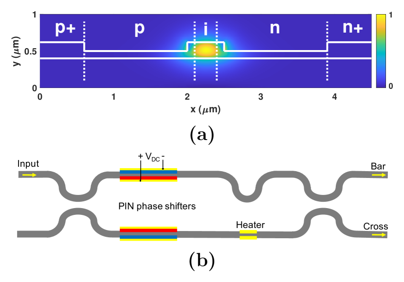
Our test structures were two MZIs with input and output adiabatic couplers, 4.5-mm-long integrated PIN junction modulators in both arms, and a path length difference of 37.4 m between the arms (Fig. 1). (One arm of each MZI also had an embedded thermo-optic phase shifter which was not used in this experiment.) The devices were fabricated in a CMOS foundry (at SUNY Polytechnic Institute) using silicon-on-insulator wafers following the design in Timurdogan et al. (2017). The modulators consisted of 500 nm 220 nm silicon ridge waveguides with embedded PIN junctions. The widths of the intrinsic silicon regions of the waveguide core of the devices were 300 nm and 400 nm, respectively. The p and n regions were formed by boron difluoride (BF2) and arsenic (As) implants with a target doping concentration of cm-3, and the p+ and n+ regions by BF2 and phosphorus (P) implants with a target doping concentration of cm-3. Tungsten vias contacting the n+ and p+ regions provided electrical connections to copper routing layers and on-chip copper contact pads. We present the experimental results from the 300 nm intrinsic silicon device in the main body of the paper and the results from the 400 nm intrinsic device in Appendix A.
III Experimental Procedure
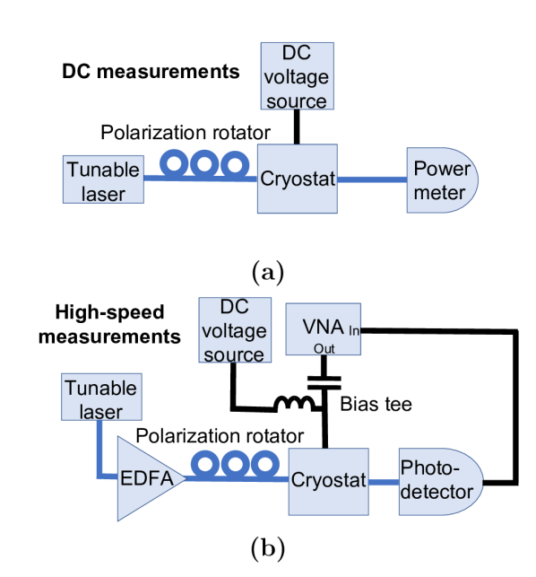
We affixed the chip with the test structures to a copper mount with conductive silver paint (Ted Pella) and wire-bonded it to a high-frequency PCB. We mounted the package in a closed-cycle cryostat (Montana Instruments) and connected the PCB to the cryostat’s RF feed-throughs. Using piezo-driven positioners, we edge-coupled lensed single-mode fibers to the input and output adiabatic couplers of the Mach-Zehnder devices (with a measured loss of 6 dB per facet). Appendix B shows the experimental setup with the packaged chip mounted in the cryostat.
Fig. 2 shows the two experimental configurations for measurements conducted with DC reverse bias only and DC bias with AC small signal, respectively. We conducted transmission measurements at room temperature and at 5 K. An Agilent tunable telecom laser (1 mW) was coupled through the input lensed fiber onto the on-chip waveguide, and polarization rotators were used to match the input to the fundamental waveguide TE mode as closely as possible. For DC measurements, we applied voltages (with an Agilent DC power supply) to reverse bias the modulator on one arm of each device at a time, and measured (with an Agilent telecom power meter) the transmitted power from one output arm of the adiabatic coupler at a time (Fig. 2a).
To conduct high-frequency measurements for determining the Mach-Zehnder bandwidths, we amplified the input laser with an Oprel erbium-doped fiber amplifier (EDFA) to provide 5 mW of on-chip power, and applied a 0.1 V AC small signal with frequencies up to 4 GHz using a Keysight vector network analyzer (VNA) (Fig. 2b). The devices were biased at their quadrature points using the DC power supply. The transmitted optical signal was routed to a Discovery Semiconductors high-speed photodetector, the electrical output of which was in turn routed to the VNA to capture the RF bandwidth of the devices.
IV Results
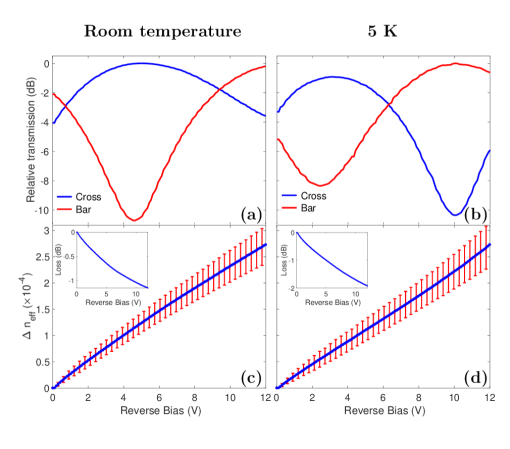
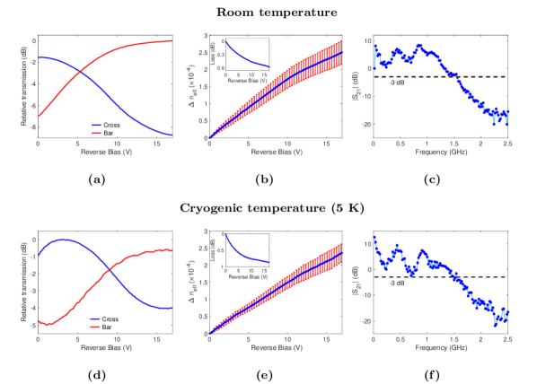
Experimental results for the 300 nm intrinsic silicon device are presented in Figs. 3 and 4, and the corresponding results for the 400 nm device in Appendix A. Figs. 3a and 3b show the transmitted power from both cross and bar arms at a representative wavelength of 1548 nm for the 300 nm intrinsic silicon MZI at room temperature and at 5 K, respectively. To determine the shift in the effective refractive index at each wavelength as a function of the DC reverse bias, we set the laser input to each wavelength and swept the DC reverse bias on one PIN modulator from 0 V to 12 V for the 300 nm device and 0 V to 17 V for the 400 nm device. The transmission curves showing both a peak and a trough in the applied voltage range were normalized and fitted to a cosine function to extract the differential phase shift as a function of the reverse bias voltage. From this empirically-estimated differential phase shift , we calculated the effective index shift as , where is the input wavelength and the PIN modulator length (4.5 mm).
In Fig. 3c, we show the average effective index shift obtained from voltage sweeps at wavelengths of 1525-1575 nm for the 300 nm intrinsic silicon device at room temperature. Fig. 3d shows the corresponding results at 5 K. The figure insets show the average relative loss as a function of applied DC reverse bias. With increasing reverse bias, the widening of the depletion region leads to a smaller overlap of the optical mode with free carriers, thus reducing the propagation loss. From our results for both the devices, we observe that the magnitudes of the effective index shifts at 5 K remain comparable to those at room temperature, exceeding 2 at the upper ends of the applied reverse bias ranges. The order of magnitude of our experimentally-obtained effective index shifts are in agreement with the simulations presented in Appendix C. These experimental results suggest that the DC Kerr effect, as well as the plasma dispersion effect, continues to remain at work down to a temperature of 5 K.
Fig. 4 shows the electro-optic frequency response of the 300 nm intrinsic silicon device reverse biased at the quadrature point at room temperature and 5 K, respectively. The 3 dB bandwidths exceed 1.5 GHz at both room temperature and 5 K. Preliminary measurements conducted using an RF probe at room temperature (before the chip was wire-bonded to the PCB) yielded higher RC-limited bandwidths (4 GHz), indicating that the chip-PCB packaging ultimately limits the speed of modulation in this experiment. By modifying the electrical packaging in future experiments to overcome the PCB-induced limitation, the devices could be operated at higher speeds up to their full intrinsic bandwidths.
V Conclusion and Outlook
In this work, we have demonstrated DC-Kerr-effect-based modulation in silicon at a cryogenic temperature of 5 K. We studied the electric field-induced refractive index shift in Mach-Zehnder modulators with embedded PIN phase shifters, and showed that effective refractive index shifts greater than 2 10-4 can be achieved at both room temperature and 5 K. The total index shift is the result of a combination of the DC Kerr and plasma dispersion effects.
Silicon DC Kerr modulators such as the ones demonstrated in this work can be fabricated in commercial silicon photonics foundries without the need for complex fabrication processes involving heterogeneous integration of electro-optic materials Eltes et al. (2018); Alexander et al. (2018); Koeber et al. (2015). However, scaling up photonic quantum technologies to a level where they can tackle practical problems in quantum simulation Aspuru-Guzik and Walther (2012) and machine learning Steinbrecher et al. (2019) and ultimately demonstrate a quantum advantage Aaronson and Arkhipov (2011); Harrow and Montanaro (2017), will likely require the co-integration of photonics with CMOS electronics Atabaki et al. (2018); Kim et al. (2019). The use of CMOS driving electronics will bring with it new challenges for the large-scale control of DC Kerr modulators. Rigorous engineering of modulator geometries will be essential for maximizing the induced effective by applying transverse electric fields approaching the breakdown field of silicon (40 V/m) while minimizing losses due to free carrier absorption. DC Kerr modulators in other CMOS-compatible platforms, such as silicon nitride (Si3N4), could also be explored as a pathway to cryogenic phase modulation in photonic integrated circuits. Recently, the photogalvanic effect in Si3N4 microring resonators has been shown to build up a DC field which in turn induces a second-order nonlinearity for highly efficient second harmonic generation Lu et al. (2020). A similar photogalvanic approach could potentially enable DC-Kerr-based phase modulation in Si3N4 or silicon-rich Si3N4 waveguides at cryogenic temperatures. Our low-temperature, high-speed DC Kerr modulator demonstration now paves the way for the use of such devices in cryogenic quantum and classical computing systems.
Acknowledgements: U.C. is supported by a National Defense Science and Engineering Graduate (NDSEG) Fellowship. J.C. is supported by EU H2020 Marie Sklodowska-Curie Grant Number 751016. Experiments were supported in part by AFOSR grant FA9550-16-1-0391, supervised by G. Pomrenke. Devices were fabricated under the Defense Advanced Research Projects Agency (DARPA) DODOS program (Grant No. HR0011-15-C-0056). This work was supported in part by the MITRE Quantum Moonshot Program. We are grateful to Gerald Gilbert, Michael Fanto, Michael Walsh, Ryan Hamerly, and Carlos Rios Ocampo for helpful discussions and comments.
References
- Wang et al. (2020) J. Wang, F. Sciarrino, A. Laing, and M. G. Thompson, Nature Photonics 14, 273 (2020).
- Hochberg and Baehr-Jones (2010) M. Hochberg and T. Baehr-Jones, Nature Photonics 4, 492 (2010).
- Carolan et al. (2015) J. Carolan, C. Harrold, C. Sparrow, E. Martín López, N. J. Russell, J. W. Silverstone, P. J. Shadbolt, N. Matsuda, M. Oguma, M. Itoh, G. D. Marshall, M. G. Thompson, J. C. F. Matthews, T. Hashimoto, J. L. O’Brien, and A. Laing, Science 349, 711 (2015).
- Sibson et al. (2017) P. Sibson, C. Erven, M. Godfrey, S. Miki, T. Yamashita, M. Fujiwara, M. Sasaki, H. Terai, M. G. Tanner, C. M. Natarajan, et al., Nature Communications 8, 1 (2017).
- Bunandar et al. (2018) D. Bunandar, A. Lentine, C. Lee, H. Cai, C. M. Long, N. Boynton, N. Martinez, C. DeRose, C. Chen, M. Grein, et al., Physical Review X 8, 021009 (2018).
- Silverstone et al. (2016) J. W. Silverstone, D. Bonneau, J. L. O’Brien, and M. G. Thompson, IEEE Journal of Selected Topics in Quantum Electronics 22, 1 (2016).
- Rudolph (2017) T. Rudolph, APL Photonics 2, 030901 (2017).
- Kim et al. (2020) J.-H. Kim, S. Aghaeimeibodi, J. Carolan, D. Englund, and E. Waks, Optica 7, 291 (2020).
- Elshaari et al. (2020) A. W. Elshaari, W. Pernice, K. Srinivasan, O. Benson, and V. Zwiller, Nature Photonics 14, 285 (2020).
- Dibos et al. (2018) A. Dibos, M. Raha, C. Phenicie, and J. D. Thompson, Physical Review Letters 120, 243601 (2018).
- Najafi et al. (2014) F. Najafi, J. Mower, N. C. Harris, F. Bellei, A. Dane, C. Lee, X. Hu, P. Kharel, F. Marsili, S. Assefa, K. K. Berggren, and D. Englund, Nature Communications 6, 1 (2014).
- Shibata et al. (2019) H. Shibata, T. Hiraki, T. Tsuchizawa, K. Yamada, Y. Tokura, and S. Matsuo, Superconductor Science and Technology 32, 034001 (2019).
- Youssefi et al. (2020) A. Youssefi, I. Shomroni, Y. J. Joshi, N. Bernier, A. Lukashchuk, P. Uhrich, L. Qiu, and T. J. Kippenberg, arXiv preprint arXiv:2004.04705 (2020).
- Shainline et al. (2018) J. M. Shainline, S. M. Buckley, A. N. McCaughan, J. Chiles, A. Jafari-Salim, R. P. Mirin, and S. W. Nam, Journal of Applied Physics 124, 152130 (2018).
- Holmes et al. (2013) D. S. Holmes, A. L. Ripple, and M. A. Manheimer, IEEE Transactions on Applied Superconductivity 23, 1701610 (2013).
- Gimeno-Segovia et al. (2017) M. Gimeno-Segovia, H. Cable, G. J. Mendoza, P. Shadbolt, J. W. Silverstone, J. Carolan, M. G. Thompson, J. L. O’Brien, and T. Rudolph, New Journal of Physics 19, 063013 (2017).
- Laing et al. (2010) A. Laing, A. Peruzzo, A. Politi, M. R. Verde, M. Hadler, T. C. Ralph, M. G. Thompson, and J. L. O’Brien, Applied Phyics Letters 97, 211109 (2010).
- Reed et al. (2010) G. T. Reed, G. Mashanovich, F. Y. Gardes, and D. J. Thomson, Nature Photonics 4, 518 (2010).
- Timurdogan et al. (2014) E. Timurdogan, C. M. Sorace-Agaskar, J. Sun, E. S. Hosseini, A. Biberman, and M. R. Watts, Nature Communications 5, 1 (2014).
- Pérez-Galacho et al. (2015) D. Pérez-Galacho, D. Marris-Morini, E. Cassan, C. Baudot, J.-M. Fédéli, S. Olivier, F. Boeuf, and L. Vivien, in 2015 17th International Conference on Transparent Optical Networks (ICTON) (IEEE, 2015) pp. 1–4.
- Harris et al. (2014) N. C. Harris, Y. Ma, J. Mower, T. Baehr-Jones, D. Englund, M. Hochberg, and C. Galland, Optics Express 22, 10487 (2014).
- Komma et al. (2012) J. Komma, C. Schwarz, G. Hofmann, D. Heinert, and R. Nawrodt, Applied Physics Letters 101, 041905 (2012).
- Gehl et al. (2017) M. Gehl, C. Long, D. Trotter, A. Starbuck, A. Pomerene, J. B. Wright, S. Melgaard, J. Siirola, A. L. Lentine, and C. DeRose, Optica 4, 374 (2017).
- Pires et al. (1990) R. Pires, R. Dickstein, S. Titcomb, and R. Anderson, Cryogenics 30, 1064 (1990).
- Faruque et al. (2018) I. I. Faruque, G. F. Sinclair, D. Bonneau, J. G. Rarity, and M. G. Thompson, Optics Express 26, 20379 (2018).
- Carolan et al. (2019) J. Carolan, U. Chakraborty, N. C. Harris, M. Pant, T. Baehr-Jones, M. Hochberg, and D. Englund, Optica 6, 335 (2019).
- He et al. (2019) M. He, M. Xu, Y. Ren, J. Jian, Z. Ruan, Y. Xu, S. Gao, S. Sun, X. Wen, L. Zhou, et al., Nature Photonics 13, 359 (2019).
- Eltes et al. (2019) F. Eltes, G. E. Villarreal-Garcia, D. Caimi, H. Siegwart, A. A. Gentile, A. Hart, P. Stark, G. D. Marshall, M. G. Thompson, J. Barreto, et al., arXiv preprint arXiv:1904.10902 (2019).
- Jacobsen et al. (2006) R. S. Jacobsen, K. N. Andersen, P. I. Borel, J. Fage-Pedersen, L. H. Frandsen, O. Hansen, M. Kristensen, A. V. Lavrinenko, G. Moulin, H. Ou, et al., Nature 441, 199 (2006).
- Chmielak et al. (2011) B. Chmielak, M. Waldow, C. Matheisen, C. Ripperda, J. Bolten, T. Wahlbrink, M. Nagel, F. Merget, and H. Kurz, Optics Express 19, 17212 (2011).
- Olivares et al. (2017) I. Olivares, T. I. Angelova, A. M. Gutierrez, and P. Sanchis, in 2017 19th International Conference on Transparent Optical Networks (ICTON) (IEEE, 2017) pp. 1–4.
- Castellan et al. (2019a) C. Castellan, A. Trenti, C. Vecchi, A. Marchesini, M. Mancinelli, M. Ghulinyan, G. Pucker, and L. Pavesi, Scientific Reports 9, 1 (2019a).
- Timurdogan et al. (2017) E. Timurdogan, C. V. Poulton, M. J. Byrd, and M. R. Watts, Nature Photonics 11, 200 (2017).
- Castellan et al. (2019b) C. Castellan, R. Franchi, S. Biasi, M. Bernard, M. Ghulinyan, and L. Pavesi, Frontiers in Physics 7, 104 (2019b).
- Boyd (2020) R. W. Boyd, Nonlinear Optics (Academic press, 2020).
- Frey et al. (2006) B. J. Frey, D. B. Leviton, and T. J. Madison, in Optomechanical Technologies for Astronomy, Vol. 6273 (International Society for Optics and Photonics, 2006) p. 62732J.
- Eltes et al. (2018) F. Eltes, J. Barreto, D. Caimi, S. Karg, A. Gentile, A. Hart, P. Stark, N. Meier, M. Thompson, J. Fompeyrine, et al., in 2018 IEEE International Electron Devices Meeting (IEDM) (IEEE, 2018) pp. 23–1.
- Alexander et al. (2018) K. Alexander, J. P. George, J. Verbist, K. Neyts, B. Kuyken, D. Van Thourhout, and J. Beeckman, Nature Communications 9, 3444 (2018).
- Koeber et al. (2015) S. Koeber, R. Palmer, M. Lauermann, W. Heni, D. L. Elder, D. Korn, M. Woessner, L. Alloatti, S. Koenig, P. C. Schindler, et al., Light: Science & Applications 4, e255 (2015).
- Aspuru-Guzik and Walther (2012) A. Aspuru-Guzik and P. Walther, Nature Physics 8, 285 (2012).
- Steinbrecher et al. (2019) G. R. Steinbrecher, J. P. Olson, D. Englund, and J. Carolan, npj Quantum Information 5, 1 (2019).
- Aaronson and Arkhipov (2011) S. Aaronson and A. Arkhipov, in Proceedings of the 43rd annual ACM symposium on Theory of computing (ACM, 2011) pp. 333–342.
- Harrow and Montanaro (2017) A. W. Harrow and A. Montanaro, Nature 549, 203 (2017).
- Atabaki et al. (2018) A. H. Atabaki, S. Moazeni, F. Pavanello, H. Gevorgyan, J. Notaros, L. Alloatti, M. T. Wade, C. Sun, S. A. Kruger, H. Meng, et al., Nature 556, 349 (2018).
- Kim et al. (2019) T. Kim, P. Bhargava, C. V. Poulton, J. Notaros, A. Yaacobi, E. Timurdogan, C. Baiocco, N. Fahrenkopf, S. Kruger, T. Ngai, et al., IEEE Journal of Solid-State Circuits 54, 3061 (2019).
- Lu et al. (2020) X. Lu, G. Moille, A. Rao, D. Westly, and K. Srinivasan, arXiv preprint arXiv:2003.12176 (2020).
- Soref and Bennett (1987) R. A. Soref and B. R. Bennett, IEEE Journal of Quantum Electronics 23, 123 (1987).
- Cheung (2020) N. Cheung, Ion Implantation, EE 143 Lecture 8 (2010; accessed April 4, 2020), http://www-inst.eecs.berkeley.edu/~ee143/fa10/lectures/Lec_08.pdf.
Appendix A Experimental results of the 400 nm device
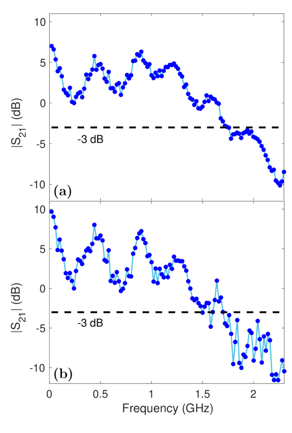
Fig. A.1 presents the experimental results of the 400 nm device. The magnitude of the overall effective index shift at 5 K remains comparable to that at room temperature.
Appendix B Experimental configuration
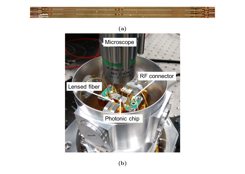
Fig. B.1a shows the section of the chip containing the Mach-Zehnder devices tested in this work. The packaged chip is shown mounted in the cryostat in Fig. B.1b. Wire bonds connect the electrical contact pads on the chip to the PCB’s shielded RF signal lines, which have SMP connector terminations. Mini-SMP cables (5 GHz bandwidth) connect the PCB to the cryostat’s RF ports for electrical control, and lensed fibers are edge-coupled to the chip facets for optical measurements.
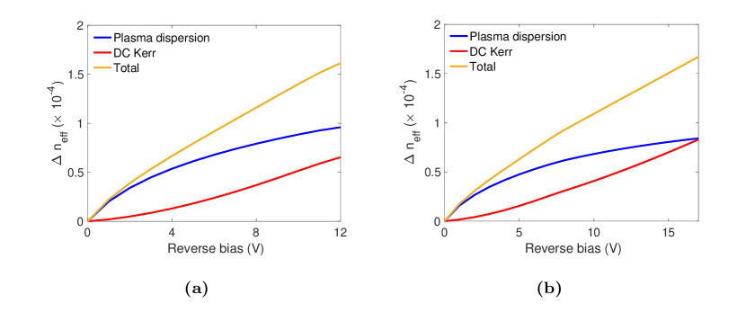
Appendix C Simulation of effective index shifts
The overall effective index shift can be obtained as the sum of the index shifts due to the DC Kerr effect and the plasma dispersion effect. We used the Lumerical CHARGE transport solver to simulate the plasma dispersion effect in our devices according to the Soref-Bennett model Soref and Bennett (1987). Owing to the unavailability of exact information on the dopant implantation parameters for the devices, we approximated the doped regions as having Pearson IV doping profiles with representative parameters based on standard dopant implantation processes Cheung (2020). The DC Kerr effect was simulated using the Lumerical FEEM waveguide solver, with the DC-Kerr-induced shift in the refractive index of silicon given by Equation (4) in the main body of the paper, and the third-order nonlinear susceptibility = 2.45 10-19 m2V-2 (as in Timurdogan et al. (2017)). The effective index shifts are plotted as a function of increasing reverse bias in Fig. C.1. These simulations provide a qualitative, order-of-magnitude confirmation of the nature of the experimentally-observed index shifts. (Since the exact magnitudes of the index shifts are highly sensitive to the implantation profile, it is not possible to obtain a more exact comparison without knowing the actual dopant implantation profiles of the devices.) While the plasma dispersion-induced index shift is expected to exhibit a dependence close to the square root of the reverse bias voltage, the DC-Kerr-induced index shift is expected to increase quadratically with voltage, producing a total index shift that increases pseudo-linearly with voltage.