A study of radiation tolerance in optical cements
Abstract
We study the effect ionizing radiation has on light transmission in the wavelength range 190–1100 nm for a number of optically clear epoxies. We find that the transmittance of traditional, commercially available, optical epoxies show significant degradation for exposures of MIPs/cm2. Degradation of light transmission progresses from the shortest wavelengths at low doses to longer wavelengths as the dose increases. In epoxy joints that are 0.1 mm thick, we observe that more than 5% of the light is lost for wavelengths less than 400 nm for traditional optical epoxies. Our studies have identified an optically clear epoxy that shows little degradation for radiation exposures up to MIPs/cm2 ( kGy).
FERMILAB-PUB-20-276-E
1 Introduction
Plastic scintillators and light sensors have a long tradition for measuring radiation in particle and nuclear physics. Speed, linearity, ability to cover large areas with low channel count and ability to machine into complex shapes have made this technology a good choice for large detector systems [1]. Current and proposed experiments that run at high radiation exposure rates and over long experiment lifetimes mean that detector systems must survive ever more hostile radiation environments. Considerable information is available in the literature that characterizes radiation tolerance of scintillator materials [2, 3] and photosensors [4, 5, 6]. However, much less information is available on the radiation tolerance of optical coupling compounds that connect scintillators and their sensors [7, 8, 9, 10]. Our observations from actual devices operating in high radiation environments are that the adhesive in the joints are visually darker than either the plastic scintillator or acrylic light guide material. In this paper we explore the radiation tolerance of a variety of commercially available, optically clear epoxies. We wish to identify candidate clear epoxies with improved radiation tolerance for light transmission in the wavelength region 190–1100 nm.
The ideal optical epoxy would have good adhesion and bond strength, transmit light in the optical region, similar refractive index as the materials used to make the detectors, and a reasonable open time to allow for assembling the detectors before the adhesive agent hardens. For this initial study, we chose a few epoxies with the following properties:
-
•
Readily available from commercial vendors.
-
•
The epoxy is advertised as clear.
-
•
Bond strength of at least 100 kg/cm2.
-
•
Working time greater than 10 minutes.
-
•
If known, a refractive index of approximately 1.5.
For comparison we chose two commercially available optical epoxies designed for use with plastic scintillator materials, BC-600 epoxy from Saint-Gobain [11] and EJ-500 from Eljen Technologies [12]. We purchased two epoxies from System 3 [13], a general purpose marine epoxy333The general purpose epoxy has three choices for hardener, 15, 30, and 60 minute working times for hardeners 1,2 and 3 respectively. We use the medium cure time hardener (2) for the tests reported in this article. and a clear coating epoxy "Mirror Coat". Finally, we purchased two epoxies from Hysol [14], E-30CL and U-09FL.
While most manufacturers offer considerable technical information on their epoxies, one parameter often missing for optical applications is the refractive index (R.I.). The refractive index of the epoxy being of critical importance to minimize Fresnel losses at the interfaces between differing optical media. We measure the refractive index of all cured epoxy samples using a Vee Gee model C10 Abbe refractometer [15]444We note that the monobromonapthalene liquid typically used to optically couple the sample to the glass in the refractometer is a solvent for many plastics and epoxies.. All refractive indices were measured at a single wavelength of 589 nm. Table 1 summarizes physical properties of epoxies included in the studies reported here. For more details on the epoxies we refer to the technical data sheets available from the manufacturers.
| Work | Hard. | Mixed | Bond | ||||
|---|---|---|---|---|---|---|---|
| Time | Time | Visc. | Stren. | Spec. | |||
| Name | Abbr. | R.I. | (min) | (hrs) | (cps) | () | Grav. |
| BC-600 [11] | BC | 1.571 | 180 | 24 | 800 | 125 | 1.18 |
| EJ-500 [12] | EJ | 1.574 | 60 | 24 | 800 | 125 | 1.17 |
| S3:MirrorCoat [13] | S3MC | 1.561* | 40 | 72 | 700 | N/A | 1.14* |
| S3:General [13] | S3GP | 1.567* | 30 | 6 | 1100 | 527 | 1.10 |
| H:E-30CL [14] | HECL | 1.520* | 30 | 2.6 | N/A | 560 | 1.07 |
| H:U-09FL [14] | HUFL | 1.49* | 10 | 3 – 24 | N/A | 194 | 1.0 – 1.2 |
The different epoxies were tested for compatibility with a standard poly(vinyltoluene) scintillator (Eljen EJ-200). The new epoxies were prepared and poured into one of two 1.91 cm diameter forms attached to a piece of scintillator. The other form was filled with EJ-500 epoxy. Once the epoxies were cured, the sample was stored in a cabinet for future examination. After over a year had elapsed, the scintillator pieces were examined under a microscope and the two sample areas compared specifically by looking for changes in the scintillator at the epoxy/scintillator interface, eg. discoloration, micro-cracks (crazing). For all epoxies studied here, we were unable to observe any degradation of the scintillator epoxy interface.
2 Sample Preparation
Optical cement samples were carefully prepared in two batches separated by 1 year using the prescription described below. To ensure uniform sample sizes and geometries, forms were made by cutting 19 mm (3/4 inch) ID clear schedule 40 PVC pipe into 9.53 mm long sections. The cut edges of each form were sanded smooth and cleaned with ethanol. A thin mylar sheet was then taped to a glass plate to provide a flat surface to which the forms would be affixed. The forms were then glued to the mylar using a cyanoacrylate adhesive and allowed to cure while the optical epoxies were prepared. All handling of any material contacting a sample during preparation or handling of a sample as described below was performed with gloves and tweezers to avoid contamination.
Sufficient optical epoxy was mixed to make 8–12 samples, approximately 50 ml total. All optical cements, epoxies were mixed according to their manufacturer’s instructions. To remove air bubbles, each mixture was placed in a centrifuge and run at 3,200 rpm for 5 minutes. After the centrifuge the clear adhesive was poured into the forms so that a meniscus protruded above the top of each form. The epoxy samples were allowed to cure for several days.
Once the samples had cured, the forms were pealed from the mylar and each epoxy sample removed from its form. A label was then written on the cylindrical portion of each sample in indelible ink. An orientation line was also filed into the cylindrical edge. Each sample was then cut and diamond polished on both sides to approximately 7 mm thick. We note that the samples are thick compared with typical glue joints of approximately 0.1 mm thickness. We will address the thickness issue in a later section. The HUFL epoxy has a cured consistency similar to silicone rubber. Without substantial additional handling and possible contamination, the HUFL samples could not be diamond polished and therefore are thicker than the samples for other epoxies. The thickness of each sample was measured in multiple places and an average thickness determined. Fractional variation of sample thicknesses for any given epoxy ranged between 0.5% to 6%. The average fractional thickness variation between different epoxies is 10% if the HUFL samples are included and 0.5% if the HUFL samples are excluded. All prepared samples were then cleaned with ethanol and the label re-applied as needed. Table 2 summarizes the sample thicknesses.
| Sample thickness (mm) | ||||||
| ID | BC | EJ | S3MC | S3GP | HECL | HUFL |
| 1 | 7.57 | 7.57 | 7.47 | 7.49 | – | – |
| 2 | 7.57 | 7.65 | 7.62 | 7.57 | – | – |
| 3 | 7.62 | 7.54 | 7.54 | 7.59 | – | – |
| 4 | 7.57 | 7.32 | 7.54 | 7.54 | – | – |
| 5 | 7.57 | 7.57 | 7.57 | 7.09 | – | – |
| 6 | 7.59 | 7.19 | 7.59 | 7.24 | – | – |
| 21 | 7.62 | 7.62 | 7.67 | 7.67 | 7.62 | 10.01 |
| 22 | 7.65 | 7.65 | 7.61 | 7.53 | 7.38 | 8.81 |
| 23 | 7.66 | 7.61 | 7.04 | 7.62 | 7.67 | 10.03 |
| 24 | 7.66 | 7.61 | 7.61 | 7.67 | 7.62 | 9.40 |
| 25 | – | – | 7.62 | – | – | – |
| 26 | – | – | 7.62 | – | – | – |
| Avg | 7.61 | 7.53 | 7.54 | 7.50 | 7.57 | 9.56 |
| Stdev | 0.04 | 0.15 | 0.17 | 0.19 | 0.13 | 0.58 |
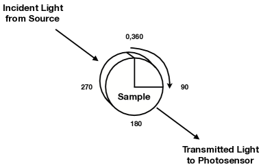
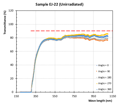
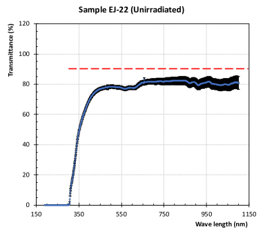
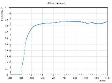
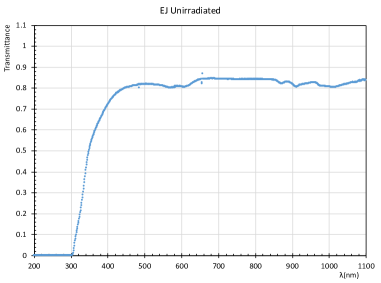
After preparation, the transmittance spectrum of each sample was measured using an Agilent Technologies spectrophotometer [16]. Transmittance is defined as ratio of light intensity passing through the material to the incident intensity. The transmittance measurements covered the wavelength range 190 nm–1100 nm in 1 nm steps using a 0.5 s integration time for the optical sensor. The data were converted to a comma separated value format for subsequent analysis. These spectra give an initial evaluation of the transmittance spectrum for each epoxy before irradiation. Transmittance measurements were made of each sample in 5 different orientations, each 90 degrees from the others. By doing so we sample the same orientation twice to check consistency of the measurements. The transmittance results of the different orientations are averaged to give a single value for each wavelength and the RMS of the measurements were calculated. Figure 1 shows the sample orientations for the measurements described above. Representative transmittance curves are shown in Figure 2 for EJ-500 optical cement555The slight double absorption in the transmittance around 550 – 600 nm appears to be a bluish tint in the resin. We see this to a greater/lesser extent in both BC-600 and EJ-500, depending on lot number.. The narrow feature at 600 nm appears in all transmittance measurements and is assumed to be a feature of the spectrophotometer. We note that typical, raw measurements plateau with a transmittance approximately 0.80 - 0.87. Given the refractive indexes of the epoxies at 589 nm, we expect Fresnel losses due to reflection at the air/material/air interfaces for ideal transmittance of 0.90–0.92. The difference between our measurements and the ideal are attributed to small imperfections in sample production. Observed imperfections in the samples fall into two broad categories and depend on sample material. For most samples, we observe "swirls" that appear to be differences in the refractive index of the material which we attribute to incomplete mixing of the resin and hardener. Modifying mixing procedures eliminates this effect. The second observed imperfection is the formation of small/microscopic bubbles in the S3GP samples during the curing process. We observe that with smaller/thinner samples, we find smaller or no bubbles. In subsequent analysis, we quote transmittance ratios for a given sample to remove the effects of imperfect sample production.
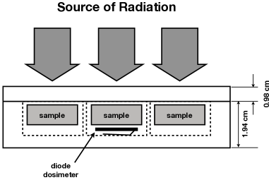
Once the initial transmittance spectrum was measured, a sample of each epoxy was loaded into a seven unit, black, delrin, sample holder. The sample holders measured 9.21 cm by 9.21 cm by 1.94 cm thick. Each sample holder had 7, 2.22 cm diameter wells 1.17 cm deep machined in a hexagonal close packed arrangement with the holes spaced 1.69 cm on center. A 0.98 cm thick delrin sheet lid held in placed with 4 stainless steel screws kept the samples from moving during irradiation. The lid was of uniform thickness. Figure 3 is a diagram of the sample holder well configuration and how the samples were loaded into the wells. A pin diode is placed under the center sample. The pin diode is used as a dosimeter to measure the particle fluence through the sample holder. The sample holders were then attached to an FR-4 strip to make a “lolly-pop” for installation in the Fermilab booster for irradiation.

3 Irradiation and Dosimetry
After preparation of the samples, the "lolly-pop" sample holders were installed in the Fermilab Booster, immediately downstream of the Booster collimators located in the straight sections of periods 6 (collimators A and B), and 7. Samples were then harvested at convenient times during accelerator down times. The radiation seen by the samples occurs from the interaction of protons accelerated in the booster that are far from the beam core interacting with the collimator material. These interactions produce an admixture of protons, neutrons, photons, electrons and pions irradiating the sample. The particle admixture means that the irradiations may stimulate a variety of possible effects in the material. This style of irradiation is ideal to survey radiation tolerance, but less than ideal to understand any specific effect.
Because the samples are exposed to a mixed radiation field, we choose to calculate a charged particle fluence for each sample’s exposure in units of minimum ionizing particles (MIPs) per cm2. For the measurements reported here we use a by 0.02 cm thick PIN diode (Hamamatsu, model S3590-08 [17]). We chose to use silicon diodes because of their observed linear increase in reverse bias current with radiation exposure over a wide range of particle fluences. As long as the particle admixture and spectrum remains constant over the exposure, this linearity is preserved and we may use a diode calibration that yields a fluence in MIPs/cm2. The change in reverse bias for a silicon diode follows the relationship,
| (3.1) |
where , are the final and initial currents, is the volume of the diode, is the charged particle fluence, the diode was exposed to and is a damage constant. We use the damage coefficient of A/cm/MIP at a temperature of 20° C derived from radiation field measurements inside the CDF detector [19]. We correct all reverse bias currents from the temperature at which the current was measured, , to a reference temperature, , of 293.15 K (20° C) using the relationship:
| (3.2) |
where is Boltzman’s constant. The factor 1.23 is the energy in eV between the valence and conduction bands for silicon.
The overall calibration of the diodes used a 137Cs source to calibrate thermal luminescent dosimeters (TLDs). The response of the TLD to MIPs was then calculated using the for LiF. The TLDs were installed inside the CDF detector tracking volume along with PIN diodes 666The original PIN diodes used in CDF were from the same wafers as the CDF silicon detector. These have the same properties as those procured later from Hamamatsu.. The PIN diode response was monitored as a function of exposure measured by the TLDs. A MARS [18] simulation confirmed that the TLDs primary response was from MIPs dominated by charged hadrons. The overall uncertainty in this calibration was found to be approximately 5% including all systematics. Details of this process may be found elsewhere [19].
The reverse bias current for a given diode is obtained by measuring its I-V curve using a program running on a laptop that controls a Keithley model 6517A electrometer [20]. The program set the bias voltage (V) and allowed the current (I) to settle for 5 seconds before recording both the applied voltage and current. The process was repeated in 10 V intervals over the range 0 – 210 V. At the time of the I-V measurements both the ambient temperature and humidity were recorded for use later. Ambient temperatures during the measurements varied over the range (18.9°– 27.7° C). Typical raw I-V curves are shown in Figure 4 for both before and after irradiation. From the measurements we calculate the change in current, after - before irradiation, for a bias voltage of 80 V for the dosimetry measurements. For the conversion from fluence (MIPs/cm2) to absorbed dose (Gy), we use the value of for acrylic as this polymer most closely matches the density of the epoxy samples.
4 Transmittance Analysis
At completion of each irradiation, the sample holders were harvested, dosimetry performed for the specific sample holder and the transmittance was measured for both the irradiated in the holder and the control samples that were unirradiated. We are interested in changes in the transmittance between when an adhesive sample was made and after its irradiation. Calculation of the ratio of the transmittance after irradiation to that measured before irradiation allows us to quantify the change in transmittance observed. However, the change in transmittance may include effects due to radiation and aging of the material. We therefore calculate the double ratio of transmittances for irradiated and unirradiated control samples using the equation:
| (4.1) |
where the are measured transmittances for each sample, , at a given absorbed dose, , and time, . The “0” dose correspond to control samples that were kept in a cabinet. The control samples saw background radiation only (mostly cosmic rays). The ratio in the denominator is the relative transmittance due to aging. The ratio in the numerator is the relative transmittance due to aging and irradiation. Figures 5 and 6 show the initial transmittance of a sample (left column) and the transmittance double ratio (right column) for the six samples studied. Uncertainties are omitted from the figures for clarity. Typical uncertainties for the transmittance and double ratio at 1100 nm are 5% and 10%, respectively.
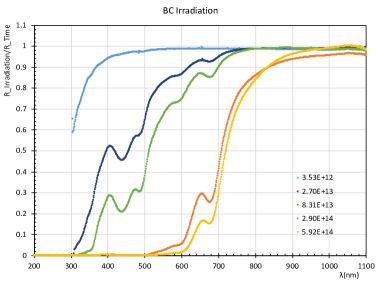
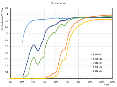
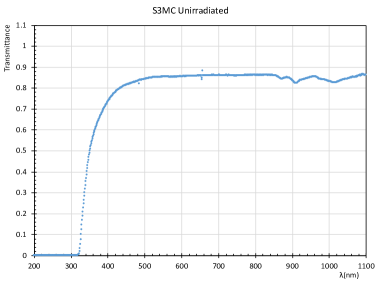
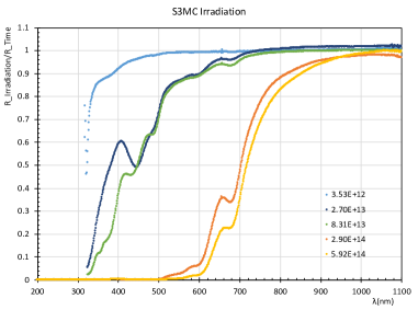
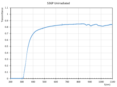
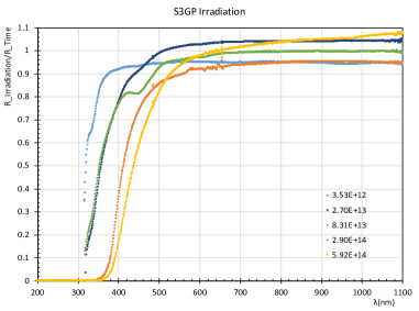
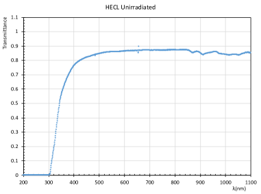
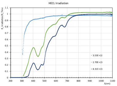
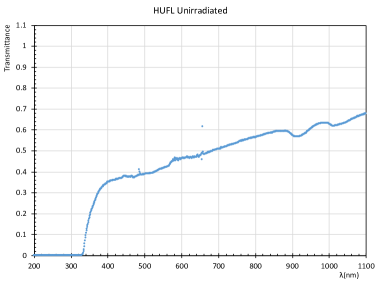
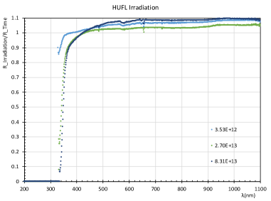
The effects of radiation show up as a loss of transmittance at short wavelengths for all samples. Higher doses leading to a loss of transmittance at longer wavelengths. Many of the spectra also show structure with two broad absorption dips in the region between 450–500 nm and another at approximately 680 nm. Two samples, S3GP and the HUFL, stand out showing less effect due to radiation. The careful reader will note that in some samples the transmittance double ratio, curve, exceeds unity at the longer wavelengths. For all samples the curves lie within the 10% uncertainty envelope quoted above. This uncertainty envelope is dominated by variations within each sample (ref, Figure 2). Because the non-uniformity is due to small, local defects this leads to a larger variation in the reproducibility for that sample. No clear pattern in the transmittance double ratio is seen with radiation exposure for any adhesive sample. For the S3GP and HUFL epoxies, the control sample had poorer transmittance and uniformity than seen in the other epoxies.
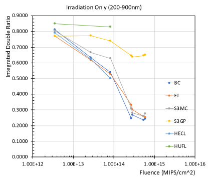
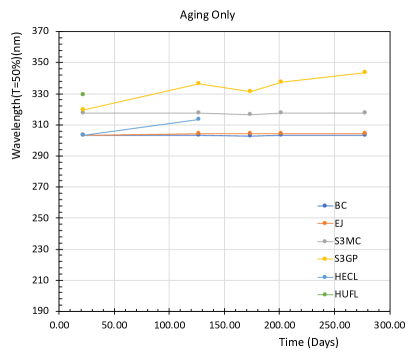
A figure of merit is needed to more compactly and directly compare the samples against one another. From the features observed, we choose to integrate the measured double ratio curve over the wavelength range 200–900 nm. The integrals are all normalized over the same wavelength range. This figure of merit represents the expected transmittance to a detector with flat sensitivity over this wavelength range. One may similarly integrate the ratio, , to extract a similar effect in the aging of the control samples. Due to the non-uniformity of the control sample, the integral hid differences in sample coloration visible by eye. Consequently, to illustrate the effects of aging we choose to quote the 50% threshold wavelength as a function of time. Figure 7 shows the double ratio integral as a function of the radiation exposure (left) and the transmittance ratio 50% threshold wavelength as a function of time for the control samples (right). The Figure shows considerably better transmittance for the two adhesives noted above. Note that the S3GP sample also shows an increase of the threshold wavelength with sample age.
Examining the samples significantly damaged during irradiation, we observe a clearing of those sample at their edges. This clearing is parallel to all sample surfaces with the clearing front extending a fraction of a mm after several months. This clearing is also observed in thin films of epoxy from detectors when a joint is broken and the epoxy is exposed to the ambient environment. The clearing of the thin film of epoxy occurs over a few days. This clearing effect is similar to that seen in plastic scintillator when exposed to air or oxygen after irradiation [21]. At this time we have not isolated the agent responsible for the effect.
5 Discussion
The samples prepared in this study are approximately 7 mm thick which is considerably thicker than a typical adhesive joint. We found that for most scintillator detectors, a typical joint thickness was 0.1 mm. Under the assumption that light absorption in the material follows a single exponential decay, for the 7 mm thick samples the amount of light lost at the 50% threshold wavelength corresponds to about 0.4% for a 0.1 mm thick adhesive joint. A 0.4% loss of light is insignificant for most measurements. Figures 5 and 6 show regions where the transmittance or double ratio is indistinguishable from zero. The Agilent spectrophotometer used for this analysis has a readout threshold for transmittance of . The threshold transmittance for the sample thicknesses approximately 7 mm thick would mean a 5% loss of light at that wavelength for the 0.1 mm thick adhesive joint. For many of the epoxy samples studied at the highest fluences, we find the transmittance below the readout threshold for wavelengths shorter than 400 nm indicating at least 5% light loss at those wavelengths. This means a substantial loss of light in the wavelength regions where typical photomultiplier tubes used in scintillator detectors have their peak quantum efficiency.
6 Summary
We have measured the radiation tolerance of a variety of commercially available optical epoxies that may be used to couple plastic scintillator to a light sensor as a function of radiation exposure. Our studies recorded the transmittance spectrum as a function of charged particle fluence measured in the mixed radiation environment near the Fermilab booster collimators. Most of the epoxies studied show reduced light transmission at short wavelengths for a given radiation exposure. When the radiation exposure is increased, transmittance at successively longer wavelengths is attenuated. For exposure fluences above MIPs/cm2, our transmittance measurements are less than the detection threshold for wavelengths below 500 nm for three of the six samples tested. Extrapolating from our 7 mm thick samples to a glue thickness of 0.1 mm means at least a 5% light loss in a real detector in the same wavelength range. However, for two of our samples, we find considerably better light transmission at wavelengths near 400 nm. One of these epoxies proved difficult to work with, HUFL. The other epoxy, S3GP, while showing signs of yellowing with age, showed little degradation for fluences up to MIPs/cm2. Our studies indicate that S3GP promises to be a good candidate for bonding scintillator to light guides and photosensors in the future, though additional studies are needed to quantify the effects of aging with this epoxy.
Acknowledgments
Work supported by the Fermi National Accelerator Laboratory, managed and operated by Fermi Research Alliance, LLC under Contract No. DE-AC02-07CH11359 with the U.S. Department of Energy, The U.S. Government retains the publisher, by accepting this article for publication, acknowledges that the United States Government retains a non-exclusive, paid-up, irrevocable, world-wide license to publish or reproduce the published form of this manuscript, or allow others to do so, for United States Government purposes.
References
- [1] W.R. Leo, Techniques for Nuclear and Particle Physics Experiments, Springer-Verlag, Berlin (1994).
- [2] C. Zorn, "Plastic and liquid organic scintillators," in: F. Sauli (Ed.), Instrumentation in High Energy Physics, 2nd Edition, World Scientific, 1993, Ch. 4, pp. 218–279.
- [3] V.Khachatryan, et al., Dose rate effects in radiation damage of the plastic scintillators of the CMS Hadron Endcap Calorimeter, JINST 11 (2016) T10004 [Erratum, ibid 14 (2019) E8001].
-
[4]
S-O. Flyckt, C.Marmonier, (editors)
Photomultiplier tubes - Principles and
applications, Photonis imaging sensors, Avenue Roger Roncier, BP 520,
19106 Brive cedex, France.
http://www.photonis.com. - [5] E. Garutti, et al., Silicon Photomultiplier characterization and radiation damage investigation for high energy particle physics applications, JINST 9 (2014) C03021.
- [6] S. Baccaro, et al., Radiation damage effect on avalanche photodiodes, Nucl. Instr. and Meth. A426 (1999).
- [7] N. Buechel, et al., Radiation Hardness Test of Eljen EJ-500 Optical Cement, arXiv 1703.10606v1 (2017).
- [8] T.Kirn, M. Haering, D.Schmitz, W.Schultz, CERN-CMS-NOTE-1999-003 (1999).
- [9] H.C. Huang, et al., Measurement of radiation damage on an epoxy based optical glue, Nucl. Instr. and Meth. A385 (1997) 559.
- [10] A. Para, G. Yasuda, E. Skup, An Investigation of the effects of Glue on Light Tranmission in Scintillating Fibers, FERMILAB-PUB-91-329, unpublished (1991).
-
[11]
Saint-Gobain, Hiram, Ohio.
https://www.crystals.saint-gobain.com. - [12] Eljen Technology, 1300 W. Broadway, Sweetwater, TX 79556.
- [13] System Three Resins, Inc, 3500W. Falley Hwy N, Suite 105, Auburn, WA 98001-2436.
-
[14]
Henkel Canada Corporation, 2515 Meadowpine Blvd,
L5N6C3 Mississauga, Ontario, CANADA.
http://www.henkel-northamerica.com. -
[15]
Vee Gee Scientific, LLC, 620 Lakeview Pkwy,
Vernon Hills, IL 60061.
https://www.veegee.com. -
[16]
Agilent Technologies, 5301 Stevens Creek Blvd.,
Santa Clara, CA 95051, USA
https://www.agilent.com. - [17] Hamamatsu Corporation, 360 Foothill Road, Bridgwater, NJ 08807.
- [18] N.V. Mokhov, Recent Mars15 developments: nuclide inventory, DPA and gas production, Fermilab-Conf-10-518C-APC(2010).
- [19] R.J. Tesarek, et al., A Measurement of the radiation environment in the CDF tracking volume, Nucl. Instrum. and Meth. A514 (2003) 188.
-
[20]
Tektronix, Inc., 14150 SW Karl Braun Drive,
P.O.Box 500, Beaverton, OR 97077, USA
https://www.tek.com. - [21] A. Bross, A. Pla-Dalmau, Radiation damage of plastic scintillators, IEEE Trans. Nucl. Sci. 39 (1992) 1199.