Quantitative near-field characterization of Surface Plasmon Polaritons on nanofabricated transmission structure
Abstract
The tailoring of plasmonic near-fields is central to the field of nanophotonics. The detailed knowledge of the field distribution is crucial for a design and fabrication of plasmonic sensors, detectors, photovoltaics, plasmon-based cicuits, nanomanipulators, electrooptic plasmonic modulators and atomic devices. We report on a fully quantitative comparison between near field observation and numerical calculations, considering the intensity distribution for TM and TE polarisations, necessary for the construction of devices in all these areas. We present the near field scanning microscopy (NSOM) results of Surface Plasmon Polaritons (SPPs), excited by linearly polarized illumination on a gold, nanofabricated transmission grating. The optimization process is performed for infrared light, for future applications in cold atoms trapping and plasmonic sensing. We show the in situ processes of build up and propagation of SPPs and confirm that the out of plane component is not coupled to the aperture-type NSOM probe.
1. Institute of Physics, Jagiellonian University in Kraków, Łojasiewicza 11, 30-348 Kraków, Poland
*aleksandra.plawecka@doctoral.uj.edu.pl
Near-field scanning microscopy (NSOM) is a well known imaging technique for optical near-field examination. Nowadays, it is one of the most powerful imaging tools thanks to a wide range of probe types and achievable subwavelength resolutions [1, 2, 3]. The technique provides a unique opportunity to investigate the physical processes such as the extraordinary optical transmission [4], light propagation in photonic crystal waveguides [5], and dynamics of plasmonic nanoantennas [6, 7]. The knowledge of the distribution of near field allows for the design of a number of devices, e.g. nanomanipulators [8, 9], sensors based on surface enhanced Raman spectroscopy [10], plasmonic sensors [11], surface plasmons-based circuits [12], electro-optic plasmonic modulators [13], and chip-scale atomic devices [14]. The understanding of near fields is necessary for the construction of structured optical potentials for cold atoms, e.g. atom mirrors and plasmonic surface traps [15, 16, 17, 18].
Surface Plasmon Polaritons (SPPs), which emerge from a coupling between the light and collective oscillations of free electrons at a metal surface, underlie a significant number of the above-mentioned experiments. The SPPs propagate along the metal-dielectric boundary, and the amplitude of the electromagnetic field is exponentially decaying in both media. The non propagating form of SPPs, Localized Surface Plasmons, are found in the vicinity of metallic nanoobjects [19]. Both forms of SPPs have been studied by NSOM technique [20, and references therein]. The research include mapping the near field associated with a metallic waveguides based on: stripes [21, 22], nanowires [23, 24], cavities [25], nanoparticles [26, 27], or gold film surface covered with randomly positioned scatterers [28, 29]. The plasmon modes were also imaged in gold nanorods [30], gratings [31, 32, 33], slits [34, 35, 36], metallic discontinuities [37], Au-Al heterostructure [38], and nanoholes [39, 40, 41]. Apart from localized and propagating SPPs, also the standing waves of SPPs, have been observed by NSOM technique for a variety of structures [42, and references therein], including a set of nano-slits [43, 44].
One of the available optical methods of generating SPPs, uses a grating coupler, which, unlike any prism-based configuration, allows to miniaturize the system [19]. The idea is to match the momenta of the incident light of TM polarization state and that of the SPPs. Among the wide selection of various grating types, the transmission structures are of particular interest, because it is possible to generate the SPP on both, glass-gold and gold-air boundaries. The latter is advantageous for cold atom experiments and NSOM imaging. Atomic mirrors use SPPs’ evanescent field to create a strong, repulsive potential for an atomic cloud [15, 16, 18, 17] and the presence of light on the gold-air side leads to unwanted atom-photon scattering. Likewise, it would be detected by the probe, disturbing the NSOM observation of SPPs’ themselves.
So far, only qualitative studies of the absolute
enhancement of the electromagnetic field have been presented, as we believe. Here, we present a fully
quantitative analysis of the SPPs’ excitation on nanofabricated transmission structure.
The NSOM imaging is confronted with numerical models, revealing the in situ processes of build
up and propagation of SPPs on a large-area grating coupler.
To maximize the efficiency of the excitation process, we have numerically optimized the parameters of the grating structure, i.e. grating period, slot width, and grating height, to obtain a narrow and deep plasmonic resonance, with a strong electromagnetic field enhancement above the grating surface. We focus on narrow-width slots, as proposed by Yoon [45]. The modeled grating geometry is presented in Fig. 1(a).
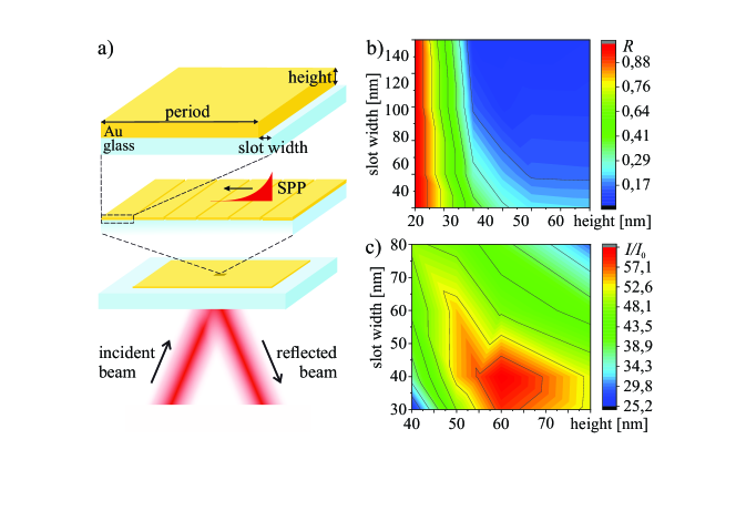
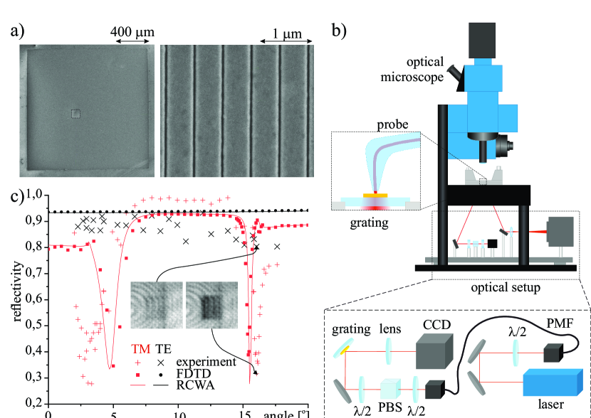
We have performed in-depth calculations of reflectivity coefficient and electromagnetic field intensity , where is the intensity of the incident light, via Rigorous Coupled Wave Analysis, see Supporting Information for more information. The most effective plasmonic resonance and electromagnetic field enhancement are obtained for grating period equal to 550 nm with reflectivity and intensity shown in Fig. 1 (b) and (c). The reflectivity coefficient is minimized for slots width 100-140 nm, and heights between 40-80 nm. On the other hand, taking into account the intensity of the electromagnetic field, we set the optimal range to 30-50 nm wide slots. Due to the technically demanding fabrication process, especially in the case of large area structures, the final parameters have been tuned so that the production errors (of the order of a few nm) do not affect the resonance significantly. Finally, 550 nm of grating period, 55 nm of grating height and 40 nm of slot width have been chosen for fabrication, and implemented in all calculations discussed in this article. The structure was nanofabricated by Focused Ion Beam (FIB) milling technique, the details are contained in Supporting Information. Directly after the FIB processing, the grating was examined in a Scanning Electron Microscope (SEM) at 5 keV electron energy in the same apparatus. The SEM images of the grating are presented in Fig. 2(a).
The detailed SEM analysis shown that the 550 nm grating period of the structure and
38 nm wide slot were achieved. In addition, presence of
spherical like shaped grains, with radius up
to 14 nm was revealed.
Measurements of the optical response of the grating were carried out using a setup shown in Fig.
2(b), details of which are described in the Supporting Information. The SPPs were excited on the
gold-air boundary and the transversal intensity distribution of the reflected light intensity was monitored on a CCD camera to control the
plasmonic resonance efficiency. At the same time, the gold-air boundary was scanned by
NSOM fiber tip to image the electromagnetic field intensity and surface topography. The presence of the SPPs is demonstrated through an extinction in the reflected
light intensity, caused by a phase difference between specularly reflected and radiated
light (see the inset in Fig. 2(c)). The measured coefficient , compared with
numerical simulations, is presented in Fig. 2
(c). The Rigorous Coupled Wave Analysis (RCWA) assumes a perfectly flat, rectangular grating, whereas the Finite Difference Time Domain (FDTD), takes into account the irregularities of the
gold surface. The minimum located around 4∘ results from the SPPs generated
on the glass-gold boundary. The second one, located around 16∘, corresponds to the SPPs excited on the gold-air edge with experimentally achieved reflectivity equal to 0.32 (coupling efficiency of 68). The narrow and deep resonance makes the grating an effective scientific tool for plasmonic sensing. The change in a refractive index of , which
is the difference between the refractive indices of air and nitrogen at 780 nm,
will result in the reflectivity decrease of 0.3, which can be easily detected
in amplitude-type sensors. A very good agreement between the simulations performed by RCWA and FDTD
methods is observed, with a mismatch in the coefficient calculated
at the optimal angle of incidence
( and ).
The difference between and quantifies the degree to which the plasmonic resonance is
deteriorated by the surface imperfections.
The periodic boundary
conditions imposed in numerical calculations make the modeled grating to be virtually
an infinite structure, are a source of discrepancies between the simulations and experimental points.
The real grating consisted of 100 m of grating
periods, surrounded by flat gold surface (hereinafter refereed to as a finite grating).
The near field distributions were imaged by NSOM, details of which are described in the Supporting Information. Scanning of the entire sample’s area and tens of m beyond was performed, with a single scan size m. For each measurement we have performed FDTD simulations, taking into account the finite size of the grating: the modelled structure consisted of 183 grating periods surrounded by 100 m of a plain gold from both sides. The surface corrugations were included in the calculations.
The analysed areas are shown in Fig. 3. We distinguish: the right edge, the center, the left edge, and outside the left edge. The light that excited SPPs illuminated the sample from the left side.
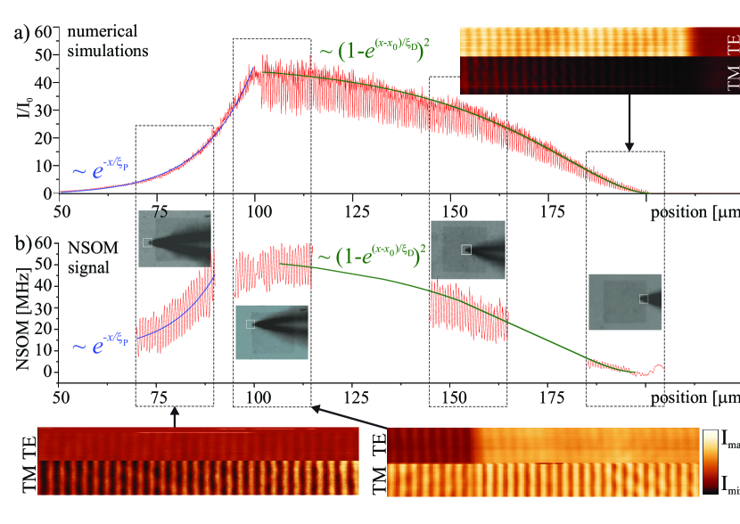
Fig. 3 (a) presents FDTD simulations of the relative intensity , for TM state of polarization, compared with the enhancement of electromagnetic field measured with NSOM exhibited in Fig. 3 (b). The scanned area is shown by the images, taken by the optical microscope, and completed with an appropriate NSOM image for both states of polarization, imaged together in a single measurement cycle (in the middle of the single m scan, the light polarization was changed). The process of SPPs’ build up takes place at the right side of the grating, demonstrated by the very low intensity for TM polarized light and poor contrast of the fringes. Then, in the middle of the grating, the signal and the contrast become stronger. The SPPs propagate even outside the left side of the grating, the enhancement of intensity reaches a factor of 50. Although the sample has no grooves outside the grating, the fringes are clearly visible – this is due to the interference between the propagating SPPs, and the incident beam, which leaks through the gold layer. Results of the numerical simulations match qualitatively the intensity distribution measured by NSOM. A quantitative agreement for the central region will be shown later. The intensity profile allows to determine the propagation length of SPP excited on the structure, which describes the distance, at which the intensity of SPPs decreases times [46]. The analytically calculated propagation length, for flat, gold surface of infinite thickness is m [46]. In the case of thin layers, apart from the always-present ohmic losses, also the leakage radiation reduces the propagation length approximately by a factor of 2, what is as confirmed in our numerical simulations for a perfect grating (no irregularities on the surface), giving m. However, to determine the propagation length in a realistic scenario, the irregularities of the grating surface must be taken into account. The exponential function has been fitted to both, numerical simulations, and NSOM signal (denoted in Fig. 3 by the blue lines). The numerically calculated propagation length is m and is consistent with the experimentally measured value m. Furthermore, the process of SPPs’ build up is investigated. Both numerical and experimental intensity profiles are very well described by an analytic formula [47] , where is the decay length. The calculated value of the decay length is m for NSOM signal, consistent with the value m from numerical simulations.
Fig. 4 compares the results obtained for different states of polarization, varying between TM (SPP presence) and TE (SPP absence) states, taken at the center of the grating.
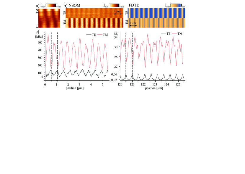
A qualitative demonstration is presented in Fig. 4 (a), showing the signal detected by NSOM, during a change of polarization state. The state was varying from TM to TE polarization, by rotating the orientation of the plane of polarization, with the step of 7.5∘. The analysis demonstrates a significant change of the intensity distribution – the maxima and minima switch their positions, and the strength of the signal weakens with decreasing SPP excitation (that is, from TM to TE). Results of NSOM measurements and FDTD simulations for TM and TE polarization states are shown in Fig. 4 (b), cross-sections allowing for a quantitative comparison are exhibited in Fig. 4 (c). Note, that the numerical simulations have been performed for the finite grating, and the results are presented for only 13 grating periods, taken from the middle of the grating. The position of minima and maxima with respect to grating’s ridges and grooves are well matched for the simulations and experiment. The maxima of the TM case occur in the middle of the ridge, while the maxima of TE polarized light can be found in the vicinity of the groove. Some discrepancies can be found in the shape of the maxima which are slightly wider in the NSOM data. This is caused by the spatial integration of the collected signal (note, that the diameter of the fiber aperture is 50 nm, excluding the Cr-Au cladding, and the width of the slot is 40 nm). Furthermore, the TM case gives stronger signal than TE, leading to a typical TM/TE ratio measured by NSOM to be 10, and the highest recorded ratio was 40. According to the FDTD simulations, the TM/TE ratio is expected to be much higher, around 500. This discrepancy, in favour of the TE polarization intensity can be readily understood. According to the Rotenberg at al, the out of plane electric field component is greatly suppressed in NSOM detection, as opposed to the in plane component, for aperture-type probes [48]. The electric field emerging from the TM polarized light has two components: and , which are the in plane, and out of plane components, respectively. The electric field arising due to the TE polarized light has only component, which is the in plane component detected efficiently by the NSOM probe. It already explains qualitatively the nature of the coupling of both polarizations to the fiber tip. A quantitative approach is shown in Fig. 5 (a) and (b). The main plasmonic enhancement is due to the component, which explains the differences between the TM/TE ratios obtained in the simulations and NSOM measurements. Results in Fig. 5 (a) show that the component (green line) is 20 times stronger than the component (blue line), so that almost completely overlaps with the total intensity distribution (red line). This is an inherent property of the SPPs on gold for the considered wavelength of 780 nm, in contrast to the case of the pure evanescent wave, where the contribution of the components may be easily varied [49]. The strong domination of the component in the NSOM results explains the well pronounced interference pattern measured outside the grating, not predicted in the simulations (compare Fig. 3 (a) and (b), left side of the grating).
The interference pattern in the glass substrate volume has an interesting origin. It comes from the interference between three waves: the incident beam, the beam reflected from the gold surface and the leakage radiation, as depicted in Fig. 5 (b) (c.f. [50]). The angle of incidence of the laser light is 15.4∘ and the angle of the leakage radiation is 43∘ in glass.
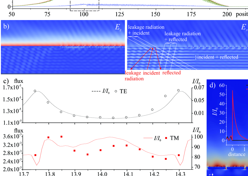
The intensity distribution above 3 grating periods and the respective cross section
are presented in Fig. 5 (d).
As expected, the exponential decay
from the surface is revealed, thus proving the usefulness of such a structure in cold atoms experiments.
In order to explain the discrepancy between FDTD intensity distribution and NSOM results,
we have taken into account the presence of the probe. Motivated by Dvořak et al.,
we have performed the Poynting flux calculations inside the fiber probe, taking into
consideration the detection of individual field components [43].
The calculation model consisted of 20 m long row of grating periods, with the
NSOM probe above them (note, that this is the infinite type of the structure;
the calculations for the finite case were infeasible.
The NSOM probe consisted of a glass structure of a 50 nm diameter, covered with 100 nm of
gold coating and was placed 15 nm above the grating structure. After calculating the flux in one
position, the simulations have been repeated for the probe shifted horizontally in 50 nm
increments, scanning more than one grating period in total. The summary is presented in Fig.
5 (c), by comparing the value of Poynting flux and the intensity distribution
(which was calculated without the NSOM probe, but for the very same 20 m of
grating periods, also for the infinite type of the grating). The
shape of the intensity distribution is indeed reproduced
for both polarization states, thus, it matches the shape of the NSOM signal. The TM to TE ratio
determined by equals 2000, while the one driven by Poynting flux gives factor
of 200, reducing the no-probe ratio ten times, giving the previously missing factor.
This proves, that the out of plane component is not detected by NSOM, and shows that
our quantitative comparison between NSOM measurement and FDTD simulations is very accurate.
In summary, we have used a NSOM technique to investigate the nature of SPPs on a
nanofabricated transmission grating. We have optimized the parameters of the grating
and we have fabricated the structure with FIB microscope. Our far field
goniometric measurements revealed the narrow and deep plasmonic resonance, with
an efficiency coupling of 68, and electromagnetic field enhancement of 50
This makes the grating an effective scientific tool for plasmonic sensing and a promising base for cold atom experiments, including precise micropotentials tailored with subwavelength resolution through SPPs excitation. The proposed transmission structure allows for the miniaturization of the system, ensures the separation between the exciting beam from the proper part of the experiment, thus can be successfully used in optical dipole mirrors, surface traps, and other plasmonic devices
[15, 16]. We have
directly observed the in situ processes of SPPs building up with the SPP decay length of m and the propagation outside the grating structure, with the propagation length equal to m. We have confirmed, that the aperture-type probe does not couple the out of plane component of the electric field. We have also quantitatively compared the signal detected by NSOM and FDTD calculation, reaching the enhancement of 50 between the excited electromagnetic field and the incident light. We have measured the intensity distribution associated with propagation of SPPs and demonstrated an accurate agreement of numerical simulations with experimental data. Our simulations also show that it is crucial to take into account the microscopic details of the structure such as the irregularities of the gold surface and the finite size of the grating for quantitative understanding of propagation and decay of SPPs. This paves the way for the full quantitative understanding of SPPs needed for a design and fabrication of plasmonic sensors, plasmon-based cicuits, photovoltaics, nanomanipulators, electrooptic plasmonic modulators and atomic devices.
We acknowledge the support of National Science Centre (doctoral scholarship – A.S.) under project 2018/28/T/ST2/00275 .
The authors thank Prof. Jakub Rysz, for lending the NSOM, his expert assistance, and useful discussions, and Prof. Franciszek Krok for the opportunity to use the SEM/FIB microscope. We also thank Dr. Jacek Fiutowski for preparing gold substrates, Dr. Paweł Dąbczyński for plasma cleaning of the grating, Dr. Dominik Wrana for SEM imaging, Dr. Dobrosława Bartoszek-Bober for contributions to the early stage of the experiment, and Dr. Piotr Sierant for remarks on the manuscript.
Supporting Information
Structure fabrication
The 55 nm thick gold layer was evaporated by electron beam metal deposition onto a glass substrate, supported by 3 nm titanium adhesion layer. The structure was fabricated by FIB milling (Dual Beam SEM/FIB Quanta 3D FEG microscope by FEI), using gallium ions of 30 keV energy, into a gold layer. The grooves are 38 nm wide and 100 m long, continuously repeated by 550 nm, on the area of 100 m 100 m. To prevent sample charging during FIB nanopatternig, electron flood gun charge neutraliser was used.
Optimization of structure parameters
The calculations for the optimization shown in Fig. 1 (b) and (c) were calculated by Rigorous Coupled Wave Analysis (RCWA), using rcwa-1d, by Pavel Kwiecien from Czech Technical University in Prague. The calculations were performed in the regime of monochromatic, near-infrared 780 nm laser light, with complex refractive index of gold equal 0.1478-4.6223, and the refractive index of glass equal 1.51. In order to avoid light diffraction into orders other than zeroth, the scanned range of the grating periods was 400-760 nm, slot widths of 30-140 nm, and grating heights of 20-80 nm. The periodic boundary conditions have been implemented in the calculations, making the grating to be virtually an infinite structure.
Numerical calculations
The near field distributions were calculated by Finite Difference Time Domain (FDTD), using commercially available EM Explorer.
Far field measurement setup
Details on the experimental setup are as follows. The 780 nm laser beam (Toptica DLX100) was guided through single mode, polarization maintaining fiber, followed by the polarizer, and reflected from the gold transmission grating from the glass-gold boundary. The presence of the plasmonic resonance was determined with CCD images, taken for TE and TM polarized laser beam. The reflectivity coefficient, , was calculated as a ratio of the intensity of the light at the grating to the intensity of the light reflected from the plain gold. The measurements were repeated for each angle separately, up to 20∘.
Near field measurement setup
The intensity of the electromagnetic field in the vicinity of the grating was measured with Nanonics MultiView 1000 Scanning Near Field Microscope. The examined area was observed in real time through an optical microscope integrated with the NSOM system. The NSOM has been working in contact, in a collection mode, with multimode Cr-Au coated fibers of two diameters: 50 and 100 nm. The collected data was analysed and compared with the AFM topography registered simultaneously by the probe.
References
- [1] D. W. Pohl, W. Denk, and M. Lanz. Optical stethoscopy: Image recording with resolution /20. Applied Physics Letters, 44(7):651–653, 1984.
- [2] U. Dürig, D. W. Pohl, and F. Rohner. Near-field optical-scanning microscopy. Journal of Applied Physics, 59(10):3318–3327, 1986.
- [3] E. Betzig, M. Isaacson, and A. Lewis. Collection mode near-field scanning optical microscopy. Applied Physics Letters, 51(25):2088–2090, 1987.
- [4] G Gay, O Alloschery, B Viaris De Lesegno, Colm O’Dwyer, J Weiner, and HJ Lezec. The optical response of nanostructured surfaces and the composite diffracted evanescent wave model. Nature Physics, 2(4):262–267, 2006.
- [5] Sergey I Bozhevolnyi, Valentyn S Volkov, Thomas Søndergaard, Alexandra Boltasseva, Peter I Borel, and Martin Kristensen. Near-field imaging of light propagation in photonic crystal waveguides: Explicit role of Bloch harmonics. Physical Review B, 66(23):235204, 2002.
- [6] Jens Dorfmuller, Daniel Dregely, Moritz Esslinger, Worawut Khunsin, Ralf Vogelgesang, Klaus Kern, and Harald Giessen. Near-field dynamics of optical Yagi-Uda nanoantennas. Nano Letters, 11(7):2819–2824, 2011.
- [7] M Schnell, A Garcia-Etxarri, AJ Huber, K Crozier, J Aizpurua, and R Hillenbrand. Controlling the near-field oscillations of loaded plasmonic nanoantennas. Nature Photonics, 3(5):287, 2009.
- [8] Alexander Minovich, Angela E Klein, Norik Janunts, Thomas Pertsch, Dragomir N Neshev, and Yuri S Kivshar. Generation and near-field imaging of Airy surface plasmons. Physical Review Letters, 107(11):116802, 2011.
- [9] Mathieu L Juan, Maurizio Righini, and Romain Quidant. Plasmon nano-optical tweezers. Nature Photonics, 5(6):349, 2011.
- [10] Jian Feng Li, Yi Fan Huang, Yong Ding, Zhi Lin Yang, Song Bo Li, Xiao Shun Zhou, Feng Ru Fan, Wei Zhang, Zhi You Zhou, Bin Ren, et al. Shell-isolated nanoparticle-enhanced raman spectroscopy. Nature, 464(7287):392–395, 2010.
- [11] Alexandre Brolo. Plasmonics for future biosensors. Nature Photonics, 6:709–713, 11 2012.
- [12] Ekmel Ozbay. Plasmonics: Merging photonics and electronics at nanoscale dimensions. Science, 311(5758):189–193, 2006.
- [13] Wenshan Cai, Justin S. White, and Mark L. Brongersma. Compact, high-speed and power-efficient electrooptic plasmonic modulators. Nano Letters, 9(12):4403–4411, 2009. PMID: 19827771.
- [14] John Kitching. Chip-scale atomic devices. Applied Physics Reviews, 5(3):031302, 2018.
- [15] Christian Stehle, Helmar Bender, Claus Zimmermann, Dieter Kern, Monika Fleischer, and Sebastian Slama. Plasmonically tailored micropotentials for ultracold atoms. Nature Photonics, 5(8):494, 2011.
- [16] Matthias Mildner, Andreas Horrer, Monika Fleischer, Claus Zimmermann, and Sebastian Slama. Plasmonic trapping potentials for cold atoms. Journal of Physics B: Atomic, Molecular and Optical Physics, 51(13):135005, 2018.
- [17] Tomasz Kawalec, Aleksandra Sierant, Roman Panas, Jacek Fiutowski, Dobroslawa Bartoszek-Bober, Leszek Jozefowski, and Horst-Gunter Rubahn. Surface plasmon polaritons probed with cold atoms. Plasmonics, 13, 03 2017.
- [18] Tomasz Kawalec, Dobrosława Bartoszek-Bober, Roman Panaś, Jacek Fiutowski, Aleksandra Pławecka, and Horst-Günter Rubahn. Optical dipole mirror for cold atoms based on a metallic diffraction grating. Opt. Lett., 39(10):2932–2935, 2014.
- [19] Stefan Alexander Maier. Plasmonics: fundamentals and applications. Springer Science & Business Media, 2007.
- [20] William L Barnes, Alain Dereux, and Thomas W Ebbesen. Surface plasmon subwavelength optics. Nature, 424(6950):824–830, 2003.
- [21] J-C Weeber, Joachim R Krenn, Alain Dereux, B Lamprecht, Yvon Lacroute, and Jean-Pierre Goudonnet. Near-field observation of surface plasmon polariton propagation on thin metal stripes. Physical Review B, 64(4):045411, 2001.
- [22] Ramona Dallapiccola, C Dubois, A Gopinath, Francesco Stellacci, and L Dal Negro. Near-field excitation and near-field detection of propagating surface plasmon polaritons on au waveguide structures. Applied Physics Letters, 94(24):243118, 2009.
- [23] Joachim R Krenn, B Lamprecht, Harald Ditlbacher, Gerburg Schider, Marco Salerno, Alfred Leitner, and Franz R Aussenegg. Non–diffraction-limited light transport by gold nanowires. EPL (Europhysics Letters), 60(5):663, 2002.
- [24] Matthias M Wiecha, Shihab Al-Daffaie, Andrey Bogdanov, Mark D Thomson, Oktay Yilmazoglu, Franko Kuppers, Amin Soltani, and Hartmut G Roskos. Direct near-field observation of surface plasmon polaritons on silver nanowires. ACS Omega, 2019.
- [25] Sinan Balci, Ertugrul Karademir, Coskun Kocabas, and Atilla Aydinli. Direct imaging of localized surface plasmon polaritons. Optics Letters, 36(17):3401–3403, 2011.
- [26] Joachim R Krenn, Alain Dereux, Jean-Claude Weeber, E Bourillot, Y Lacroute, Jean-Pierre Goudonnet, Gerburg Schider, W Gotschy, Alfred Leitner, Franz R Aussenegg, et al. Squeezing the optical near-field zone by plasmon coupling of metallic nanoparticles. Physical Review Letters, 82(12):2590, 1999.
- [27] Stefan A Maier, Pieter G Kik, Harry A Atwater, Sheffer Meltzer, Elad Harel, Bruce E Koel, and Ari AG Requicha. Local detection of electromagnetic energy transport below the diffraction limit in metal nanoparticle plasmon waveguides. Nature Materials, 2(4):229–232, 2003.
- [28] Sergey I Bozhevolnyi, Valentyn S Volkov, and Kristjan Leosson. Localization and waveguiding of surface plasmon polaritons in random nanostructures. Physical Review Letters, 89(18):186801, 2002.
- [29] Sergey I Bozhevolnyi, Valentyn S Volkov, Alexandra Boltasseva, and Kristjan Leosson. Local excitation of surface plasmon polaritons in random surface nanostructures. Optics Communications, 223(1-3):25–29, 2003.
- [30] Kohei Imura, Tetsuhiko Nagahara, and Hiromi Okamoto. Near-field optical imaging of plasmon modes in gold nanorods. The Journal of Chemical Physics, 122(15):154701, 2005.
- [31] J Jose, Franciscus B Segerink, Jeroen P Korterik, Alberto Gomez-Casado, Jurriaan Huskens, Jennifer Lynn Herek, and Herman L Offerhaus. Enhanced surface plasmon polariton propagation length using a buried metal grating. Journal of Applied Physics, 109(6):064906, 2011.
- [32] Tahir Iqbal. Propagation length of surface plasmon polaritons excited by a 1D plasmonic grating. Current Applied Physics, 15(11):1445–1452, 2015.
- [33] Mena N Gadalla, Kundan Chaudhary, Christine M Zgrabik, Federico Capasso, and Evelyn L Hu. Imaging of surface plasmon polaritons in low-loss highly metallic titanium nitride thin films in visible and infrared regimes. Optics Express, 28(10):14536–14546, 2020.
- [34] HW Kihm, Kwang Geol Lee, DS Kim, JH Kang, and Q-Han Park. Control of surface plasmon generation efficiency by slit-width tuning. Applied Physics Letters, 92(5):051115, 2008.
- [35] Prabhu K Venuthurumilli, Xiaolei Wen, Vasudevan Iyer, Yong P Chen, and Xianfan Xu. Near-field imaging of surface plasmons from the bulk and surface state of topological insulator Bi2Te2Se. ACS Photonics, 6(10):2492–2498, 2019.
- [36] D Costantini, L Greusard, A Bousseksou, R Rungsawang, TP Zhang, Ségolène Callard, J Decobert, F Lelarge, G-H Duan, Y De Wilde, et al. In situ generation of surface plasmon polaritons using a near-infrared laser diode. Nano Letters, 12(9):4693–4697, 2012.
- [37] L Salomon, G Bassou, H Aourag, JP Dufour, F De Fornel, F Carcenac, and AV Zayats. Local excitation of surface plasmon polaritons at discontinuities of a metal film: Theoretical analysis and optical near-field measurements. Physical Review B, 65(12):125409, 2002.
- [38] Tazuko Kitazawa, Shintaro Miyanishi, Yoshiteru Murakami, Kunio Kojima, and Akira Takahashi. SNOM observations of surface plasmon polaritons on metal heterostructures. Chinese Physics Letters, 24(10):2827, 2007.
- [39] L Yin, VK Vlasko-Vlasov, A Rydh, J Pearson, U Welp, S-H Chang, SK Gray, George C Schatz, DB Brown, and C Wl Kimball. Surface plasmons at single nanoholes in au films. Applied Physics Letters, 85(3):467–469, 2004.
- [40] Rongjing He, Xiuli Zhou, Yongqi Fu, and Yiwei Zhang. Near-field optical experimental investigation of gold nanohole array. Plasmonics, 6(1):171–176, 2011.
- [41] Shih-Hui Chang, Stephen K Gray, and George C Schatz. Surface plasmon generation and light transmission by isolated nanoholes and arrays of nanoholes in thin metal films. Optics Express, 13(8):3150–3165, 2005.
- [42] Fan Ye, Juan M Merlo, Michael J Burns, and Michael J Naughton. Optical and electrical mappings of surface plasmon cavity modes. Nanophotonics, 3(1-2):33–49, 2014.
- [43] Petr Dvořák, Tomáš Neuman, Lukáš Břínek, Tomáš Šamořil, Radek Kalousek, Petr Dub, Peter Varga, and Tomáš Šikola. Control and near-field detection of surface plasmon interference patterns. Nano Letters, 13(6):2558–2563, 2013.
- [44] Petr Dvořák, Zoltán Édes, Michal Kvapil, Tomáš Šamořil, Filip Ligmajer, Martin Hrtoň, Radek Kalousek, Vlastimil Křápek, Petr Dub, Jiří Spousta, Peter Varga, and Tomáš Šikola. Imaging of near-field interference patterns by aperture-type SNOM — influence of illumination wavelength and polarization state. Opt. Express, 25(14):16560–16573, 2017.
- [45] Kyung Hun Yoon, Michael L. Shuler, and Sung June Kim. Design optimization of nano-grating surface plasmon resonance sensors. Opt. Express, 14(11):4842–4849, 2006.
- [46] Heinz Raether. Surface plasmons on smooth surfaces. In Surface plasmons on smooth and rough surfaces and on gratings, pages 4–39. Springer, 1988.
- [47] Stephan T Koev, Amit Agrawal, Henri J Lezec, and Vladimir A Aksyuk. An efficient large-area grating coupler for surface plasmon polaritons. Plasmonics, 7(2):269–277, 2012.
- [48] N Rotenberg and L Kuipers. Mapping nanoscale light fields. Nature Photonics, 8(12):919, 2014.
- [49] Leszek Józefowski, Jacek Fiutowski, Tomasz Kawalec, and Horst-Günter Rubahn. Direct measurement of the evanescent-wave polarization state. JOSA B, 24(3):624–628, 2007.
- [50] Oksana Kostiučenko, Jacek Fiutowski, Tomasz Kawalec, Vladimir Bordo, Horst-Günter Rubahn, and Leszek Jozefowski. Surface plasmon polariton dispersion relation at organic/dielectric/metal interfaces. Optics Communications, 331:77–81, 2014.