Quantification of interfacial spin-charge conversion in metal/insulator hybrid structures by generalized boundary conditions
Abstract
We present and verify experimentally a universal theoretical framework for the description of spin-charge interconversion in non-magnetic metal/insulator structures with interfacial spin-orbit coupling (ISOC). Our formulation is based on drift-diffusion equations supplemented with generalized boundary conditions. The latter encode the effects of ISOC and relate the electronic transport in such systems to spin loss and spin-charge interconversion at the interface, which are parameterized, respectively, by and . We demonstrate that the conversion efficiency depends solely on these interfacial parameters. We apply our formalism to two typical spintronic devices that exploit ISOC: a lateral spin valve and a multilayer Hall bar, for which we calculate the non-local resistance and the spin Hall magnetoresistance, respectively. Finally, we perform measurements on these two devices with a BiOx/Cu interface and verify that transport properties related to the ISOC are quantified by the same set of interfacial parameters.
keywords:
American Chemical Society, LaTeXContributed equally to this work \altaffiliationContributed equally to this work \abbreviationsIR,NMR,UV
A thorough understanding of charge and spin transport is crucial for the development of devices based on the electric control of spin currents. 1, 2. In this respect, the charge-spin interconversion via spin-orbit coupling (SOC) plays a key role. SOC leads to the widely studied spin Hall (SHE) 3, 4, 5 and Edelstein (EE) effects 6, 7, 8, 9, which are at the basis of spin-orbit torque memories 10, 11, 12 and spin-based logic devices 13, 14.
Of particular interest are systems with sizable spin-charge interconversion at the interface between an insulator (I) that contains a heavy element, and a normal metal (N) with negligible SOC and long spin relaxation length, as for example BiOx/Cu bilayers. In these systems, the spin-charge interconversion occurs at the hybrid interface via an interfacial spin-orbit coupling (ISOC) 15, 16. Whereas the electronic transport in N is well described by customary drift-diffusion equations, the interfacial effects occur at atomic scales near the interface and, hence, their inclusion into the drift-diffusion model is kind of subtle. Some works use an intuitive picture based on the idealized two-dimensional Rashba model and assume the existence of a two-dimensional electron gas with Rashba SOC at the interface 16, 17, 18, in which the conversion takes place via the EE and its inverse (IEE). Such description is clearly valid for conductive surface states in (e.g. topological) insulators 19, 20 or two-dimensional electron gases 21, 22. However, in metallic systems, it requires the introduction of additional microscopic parameters to model the coupling between interface states and the diffusive motion of electrons in the metal. Moreover, the very existence of a well-defined two-dimensional interface band, and its relevance for the electronic transport, in systems like BiOx/Cu is not obvious as realistic device structures are frequently polycristalline and quite disordered. Apparently, the physical picture involving the interface band with Rashba SOC is merely one of the possible interpretations for the experimental data. One can contemplate other microscopic scenarios to describe the charge-spin coupling in I/N systems. For example, in the BiOx/Cu interface, one could assume that Bi atoms diffuse into Cu and induce an effective “extrinsic” SOC in a thin layer near the interface. Alternatively, a spin-charge interconversion can be generated via an interfacial spin-dependent scattering of the bulk Bloch states (see, for example, Refs. 23, 24, 25). Each of these models will provide a different set of microscopic parameters, which usually have to be inferred from the measurements of macroscopic transport properties.
In this Letter, we approach the problem from a different angle and propose a universal theoretical framework which is independent of microscopic mechanisms and details. Specifically, we provide the basic drift-diffusion theory describing the charge and spin transport in I/N structures. To account for the ISOC, we use the effective boundary conditions (BCs) derived in Ref. 26. In this work, such BCs basically describe two types of interfacial processes mediated by ISOC: spin-charge interconversion and spin losses, quantified respectively by the interfacial spin-to-charge/charge-to-spin conductivities, , and the spin loss conductances for spins polarized parallel/perpendicular to the interface. The efficiency of spin-charge interconversion, which is central to the development of spintronic devices, is determined by the ratio between the strengths of these two processes. This ratio coincides with the widely used conversion efficiency, the inverse Edelstein length , such that . We apply our theory to describe two typical experimental setups: a lateral spin valve (LSV) made of Cu wires with a middle wire partially covered by a BiOx layer (see Fig. 2a), where non-local resistances are measured, and a BiOx/Cu/YIG trilayer Hall bar (see Fig. 4a), where we measure the spin Hall magnetoresistance (SMR). From contrasting the experimental results with our theory, we demonstrate that , which confirms the Onsager reciprocity. In addition, both experiments can be described by similar values of the ISOC parameters when measured at the same temperature. This confirms that the spin-charge interconversion in those systems only depends on the intrinsic properties of the BiOx/Cu interface.
1 Model and method
We consider a customary setup consisting of a normal metal (N) with negligible spin-orbit coupling adjacent to a non-magnetic insulator (I), see Fig. 1. In the N layer, spin and charge transport is described by the diffusion equations:
| (1) |
| (2) |
Here, and are the spin and charge electrochemical potentials (ECP), where hat symbol indicates spin pseudovector. It is assumed that N has inversion symmetry and the spin relaxation is isotropic and described by the bulk spin diffusion length 27. The diffusive charge and spin currents are defined as and , respectively, with .
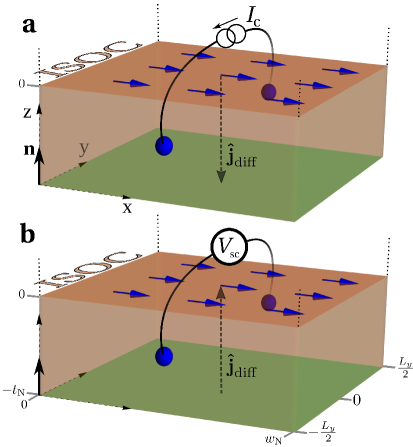
Equations (1) and (2) are complemented by boundary conditions (BCs) at the interfaces. Specifically, at the interface with vacuum, one imposes a zero current condition. Whereas, at the I/N interface with ISOC, the BCs read 26:
| (3) |
| (4) |
We denote by the vector normal to the interface, pointing from the metal towards the interface, and is the conductivity of N. Equation (3) is the BC for the spin ECP. The last term in the r.h.s. describes the charge-to-spin conversion, whose efficiency is described by the conductivity . As schematically shown in Fig. 1a, this term couples an effective electric field and the spin current density at the interface 28, 29, 30, 26, and can be interpreted as an interfacial spin Hall conductivity. Alternatively, it can be interpreted as if the charge current induces an homogeneous spin ECP via an interfacial Edelstein effect (EE), which in turn diffuses into the bulk conductor. These two interpretations are fully compatible within the present formalism. The second type of processes which take place at the interface are spin losses (first two terms in the r.h.s. of Eq. (3)), which are quantified by the corresponding spin loss conductance density per area for spins perpendicular/parallel (/) to the interface.
Equation (4) is the BC for the charge ECP. The charge is obviously conserved and, therefore, the r.h.s. only contains the spin-to-charge conversion between a diffusive bulk spin current and an interfacial charge current, which induces a voltage drop. The last term in Eqs. (3) and (4) describes reciprocal effects. 111Symmetry arguments alone cannot fix the relation between and 26. However, we will see by contrasting theory with experiment, that reciprocity requires . Equation (4) can be interpreted as an interfacial inverse spin Hall effect (ISHE), which couples the charge and the spin currents. But again, an alternative interpretation is possible: from the conservation of the charge current at the interface, we can relate the bulk charge current to the divergence of an interfacial current as . Comparing this last equation with Eq. (4), we may define the interfacial charge current density as: 222Notice that, in principle, an additional divergenceless term may appear in the r.h.s. of Eq. (5). Indeed, as demonstrated in Ref. 26, symmetry allows for a term proportional to the out-of-plane component of the spin ECP. In the present work, we only consider spin polarization parallel to the I/N interface and, hence, we neglect that term.
| (5) |
Written this way, BC (4) describes the conversion of a non-equilibrium spin into an interfacial charge current, which corresponds to what is usually called the interfacial inverse Edelstein effect (IEE), as illustrated in Fig. 1b.
Within this last interpretation, we can introduce the commonly used conversion parameter . It has dimensions of a length and is defined as the ratio between the amplitude of the induced interfacial charge current density, , and the amplitude of the spin current injected to the interface from the bulk, . From Eq. (5), one can see that the effect is finite only if the spin current is polarized in a direction parallel to the interface. By using Eqs. (3) and (5), we then obtain:
| (6) |
This is a remarkable result that follows straightforwardly from our description. is purely determined by interfacial parameters and it is indeed a quantification of the conversion efficiency since it is the ratio between the spin-to-charge conversion and the spin loss at the interface. Note that both parameters, and , are finite only in the presence of a finite ISOC. Their specific values depend on the microscopic properties of the interface, which are intrinsic for each material combination. Both and may depend on temperature and, thus, is also temperature dependent.
From an experimental perspective, the spin-to-charge conversion is usually detected electrically, by measuring a voltage drop. Typical devices are shown in Figs. 2a and 4a, where transverse voltages are measured. In theory, one needs to determine and integrate the charge ECP to determine the averaged voltage drop between two points. For concreteness, we consider the generic setup shown in Fig. 1b, in which a spin current polarized in the direction flows towards the interface, such that a voltage difference is generated in the transverse, , direction according to Eq. (5). The averaged voltage drop is measured between the points , with the total length in the direction, and is given by (see Note S1 for details):
| (7) |
where is the cross-sectional area of the wire, with and being its thickness and width, respectively, over which the voltage drop is averaged. Equation (7) shows that the voltage drop between two points is proportional to the total spin accumulation created via the ISOC between them.
In the following, we apply the above formalism to derive the voltage drop associated to spin-charge interconversions in two different devices.
Results and discussion
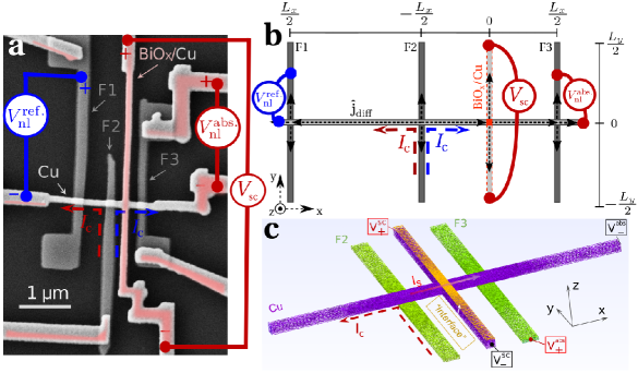
We start analyzing the double LSV shown in Fig. 2a (see Note S2 for fabrication and measurement details). A charge current is injected from the Permalloy (Py) injector F2 into a Cu wire. F2 forms a LSV either with the detector F1 or F3. We use the LSV between F2 and F1 as a reference setup. In the LSV between F2 and F3 there is an additional transverse Cu wire covered by a BiOx layer (red in Fig. 2a) and, hence, ISOC at the BiOx/Cu interface. In this case, part of the spin current in the main Cu wire is absorbed and converted to a transverse charge current (see Fig. 1b).
Quantitative description of the spin injection, diffusion, and detection in LSVs has been widely studied in the literature 31, 32. In our setup, the thickness and width of the Cu wires are much smaller than the spin diffusion length , and one can integrate the spin diffusion equation (1) over the wire cross-section and simplify it to a one-dimensional problem 32, 33, 31, as sketched in Fig. 2b. At the BiOx/Cu middle wire, the -integration using the BC at of Eq. (3), leads to a renormalization of (see Note S3):
| (8) |
where we neglect corrections of order .
At the crossing point, in Fig. 2b, we use Kirchhoff’s law for the spin currents (see Note S3):
| (9) |
Here, is the effective spin (bulk) conductance of the BiOx/Cu wire, with . The latter is the effective area of the BiOx/Cu interface that absorbs (injects) spin current. Indeed, the r.h.s. of this equation corresponds to Eq. (3) with an effective spin loss conductance counting for both the interfacial and bulk spin losses at the middle wire. The last term in Eq. (9) corresponds to the last term in Eq. (3) and it is proportional to the total injected charge current along the middle wire oriented in the direction. If we assume an homogeneously distribution of the current, then .
The Cu/Py interfaces are described by the following BC 34, 31, 35:
| (10) |
where and are the spin ECPs at ferromagnets F2 and F3, respectively. The polarization and effective conductivity at the ferromagnets are and , respectively, and is the distance between consecutive ferromagnetic wires. Since the spin current strongly decreases at the ferromagnets, corresponds to the Py/Cu junction area 31. The last term of the first equation above is proportional to the charge current density, , (homogeneously) injected at the ferromagnetic wire. For the description of the reference LSV, we substitute F3 by F1 in the second BC. Because the Py/Cu interfaces are good metallic contacts we assume the continuity of . This condition, together with the one-dimensional version of Eq. (1) and the BCs (9) and (10), determine the full spatial dependence of .
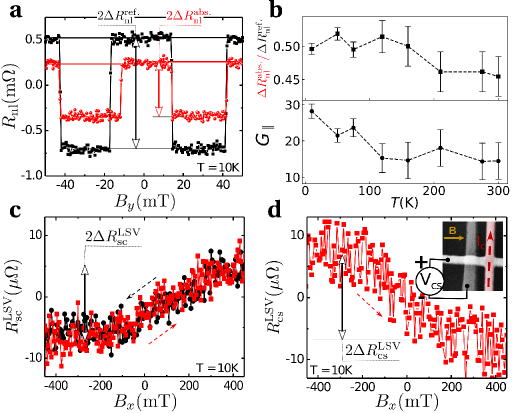
We are interested in the value of at the detectors F1/F3 which is proportional to the non-local voltages 31, 36 (see Fig. 2b). From such non-local measurement, we determine the non-local resistance, , where is the current injected from F2. The value of changes sign when the magnetic configuration of injector and detector ferromagnets changes from parallel, , to antiparallel, , which experimentally allows us to remove any baseline resistance coming from non-spin related effects by taking (see Fig. 3a). Comparing the non-local resistance measured at F3, , with the one measured at F1 at the reference LSV, , the magnitude of the spin absorption 32, 37 and, therefore, the value of the spin loss conductance, , can be obtained from our model. For this, we compute the ratio by solving the full boundary problem and obtain the following expression:
| (11) |
Here, are the spin conductances of the Cu and Py wires, with , , and , the corresponding parameters for the bare Cu wire () and the ferromagnet ( = F). The form of Eq. (11) agrees with the one obtained in previous works 37. However, our formulation is more general since it distinguishes via between interfacial and bulk losses at the BiOx/Cu wire. Consequently, we can ensure that our calculation of the ISOC parameter and, therefore, , is only related to interfacial effects (see Eqs. (6), (8), and (9)).
Interestingly, Fig. 3b shows weak temperature dependence of the absorption ratio, , revealing that about half of the spin current is absorbed at the BiOx/Cu middle wire. For the calculation of via Eq. (11), the resistivity of the Cu layer is carefully measured as a function of the temperature (see Note S4), with , and . Assuming that the magnetic properties of Py and the specific spin resistivities of Py and Cu of our device are the same as in Ref. 38, we use the same temperature dependence of and , and the constant spin resistivities and . By inserting these experimental values in Eq. (11) for different temperatures, we obtain the temperature dependence of the spin loss conductance for the BiOx/Cu interface shown in Fig. 3b. A slight decrease of can be observed with increasing temperature, which seems to arise from the Cu conductivity. A linear relation between and (see Note S5A) suggests a Dyakonov-Perel mechanism of the spin loss, expected for a Rashba interface, which also agrees with the observations of Ref. 39.
In addition, we can determine in the same device. By injecting a charge current from F2, a -polarized spin current is created and reaches the BiOx/Cu wire, where a conversion to a transverse charge current occurs via Eq. (5). This is detected as a non-local voltage along the BiOx/Cu wire and the non-local resistance is determined as a function of an in-plane magnetic field along the hard axis of F2, . By reversing the orientation of the magnetic field, the opposite is obtained, since the Py magnetization is reversed as well as the orientation of the spin polarization (see Fig. 3c). The difference of the two values for , denoted as in Fig. 3c, allows to remove any baseline resistance. By swapping the voltage and current probes, the reciprocal charge-to-spin conversion signal, , can also be measured.
Theoretically, from the calculation of the spatial dependence of the spin ECP, we compute both , from Eq. (7), and , by assuming a homogeneous spin absorption/injection at . We obtain the same expressions, with opposite sign:
| (12) |
Experimentally, Figs. 3c and 3d confirm the reciprocity between both measurements, . The broken time reversal symmetry, due to the magnetic contacts, leads to the opposite sign for reciprocal measurements. By contrasting this with the result of Eq. (12), one confirms that . The experimental value for at 10 K yields for the spin-charge conductivity and . This value is of same order of magnitude, but somewhat smaller, than previous reported results obtained by spin pumping experiments, 15, 18, 39, and LSV experiments, 33. This discrepancy might be due to a different quality of the BiOx/Cu interface: ex-situ deposition in this experiment (see Note S2) and in-situ deposition in the other works. The temperature dependence of the different parameters is presented in Note S5B. One observes a decreasing trend of by increasing the temperature, which translates in a decreasing of the Edelstein length, in agreement with previous literature 39.
In order to check the accuracy of our 1D model, we have performed a 3D finite element method simulation detailed in Note S6. Figure 2c shows the geometry of the simulated device and the mesh of the finite elements. The interface with ISOC is simulated as a thin layer with finite thickness and characterized by a spin diffusion length and an effective spin Hall angle . Using the definition of the Edelstein length as 40, we obtain nm, in good agreement with the estimated from our 1D model.
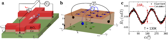
In order to verify that both ISOC parameters, and , are interface specific, we carry out an additional experiment involving a BiOx/Cu interface. Namely, we measure the SMR in a Cu layer sandwiched between a BiOx (at ) and a YIG layers (at ), shaped as a Hall bar, as shown in Fig. 4a (see Note S2 for fabrication and measurement details). In this setup, see Fig. 4b, a charge current in the longitudinal direction ( direction), induces an out-of-plane spin current density via the ISOC, described by the last term of Eq. (3). This spin current, polarized in the direction, propagates towards the Cu/YIG interface where is partly reflected and modified 41, 42, 43. The reflected spin current diffuses back to the BiOx/Cu interface, where it is converted back to an interfacial charge current via the reciprocal effect. Therefore, the overall effect is of second order in ISOC and proportional to .
YIG is an insulating ferrimagnetic material and the electron spin reflection at the Cu/YIG interface depends on the direction of magnetization of the YIG, denoted as . The effective BC describing this interface is well-known and reads as follows: 44 333Following our convention the vector normal to the interface, points from the Cu towards the insulating layer.
| (13) |
Here, are the real and imaginary parts of the spin-mixing conductance (per area), , and is the so-called spin-sink conductance. The values of these parameters are known for YIG, where and, hence, can be neglected 45, 46, 47, 43.
In the experiment, the transverse angular dependent magnetoresistance (TADMR) measurement is performed in the Hall bar of BiOx/Cu grown on a YIG substrate as shown in Fig. 4a. The transverse voltage depends on the direction of the in-plane applied magnetic field, parameterized by the angle . The experimental results for the TADMR, , are shown in Fig. 4c.
To calculate , we first determine the spatial dependence of the spin ECP from Eq. (1) and BCs Eq. (3) and Eq. (13) at the BiOx/Cu and Cu/YIG interfaces, respectively. We assume that the system is translational invariant in the – plane and reduce the diffusion problem to a 1D problem in the direction. We then use Eq. (7) to obtain , averaged in the cross-sectional area . This results in:
| (14) |
We denote by the amplitude of the modulation and assume that (see Note S7 for the exact expression). Note that the parameters of the Cu/YIG interface, , add to the spin loss at the BiOx/Cu interface . We identify by comparison of Eqs. (3) and (13) two effective spin loss conductances, and , for spins polarized in the and directions, respectively. The amplitude of the SMR signal is then, according to Eq. (14), proportional to the difference .
From Figure 4c, we estimate at K. At this temperature, from the LSV measurements, we obtain for the BiOx/Cu ISOC parameters and , as shown in Figs. 3b and S3b, respectively. The spin conductances and in light metal/YIG interfaces have been estimated in evaporated Cu and Al 48, 49. Whereas for Cu/YIG 49 is a consistent value in the literature 48, 50, the reported is very low 49, as generally observed in evaporated metals on YIG 48, 51. By substituting , , and values in Eq. (14), we obtain . This value for sputtered Cu on YIG is much larger than that estimated in evaporated Cu on YIG, in agreement with the reported difference between sputtered and evaporated Pt 51. Importantly, the obtained satisfies the required condition 43, 50 which confirms the validity of our estimation.
Conclusions
We present a complete and novel theoretical framework based on the drift-diffusion equations to accurately describe electronic transport in systems with ISOC at non-magnetic metal/insulator interfaces. Within our model, the interface is described by two type of processes: spin losses, parameterized by the interfacial conductances , and spin-charge interconversions, quantified by and . These parameters are material-specific. The efficiency of the interconversion is quantified by the ratio , which coincides with the commonly used Edelstein length . The Onsager reciprocity is directly captured by , as demonstrated by comparing our theoretical and experimental results. Our theory is an effective tool for an accurate quantification of spin-charge interconversion phenomena at interfaces, which is of paramount importance in many novel spintronic devices.
C.S-F, F.S.B., and I.V.T acknowledge funding by the Spanish Ministerio de Ciencia, Innovación y Universidades (MICINN) (Projects No. FIS2016-79464-P and No. FIS2017-82804-P), by Grupos Consolidados UPV/EHU del Gobierno Vasco (Grant No. IT1249- 19). The work of F.S.B. is partially funded by EU’s Horizon 2020 research and innovation program under Grant Agreement No. 800923 (SUPERTED). The work at nanoGUNE is supported by Intel Corporation through the Semiconductor Research Corporation under MSR-INTEL TASK 2017-IN-2744 and the “FEINMAN” Intel Science Technology Center, and by the Spanish MICINN under the Maria de Maeztu Units of Excellence Programme (MDM-2016-0618) and under project number MAT2015-65159-R and RTI2018-094861-B-100. V.T.P. acknowledges postdoctoral fellowship support from “Juan de la Cierva–Formación” program by the Spanish MICINN (grant numbers FJCI-2017-34494). E.S. thanks the Spanish MECD for a PhD fellowship (grant number FPU14/03102).
-
•
Additional details on the derivation of the spin-to-charge averaged voltage, Eq. (7), and the renormalized spin diffusion length and node boundary condition for the LSV, Eqs. (8) and (9), respectively; measured temperature dependence of the Cu resistivity and analysis on the temperature dependence of the ISOC parameters in the LSV; brief explanation of the 3D simulation and the relation between the simulation and ISOC parameters; theoretical result for the transverse resistance measured in the multilayer Hall bar, i.e., which leads to Eq. (14). The experimental details of the nanofabrication and measurements of the LSV and multilayer Hall bar devices are also included.
References
- Žutić et al. 2004 Žutić, I.; Fabian, J.; Das Sarma, S. Spintronics: Fundamentals and applications. Rev. Mod. Phys. 2004, 76, 323–410
- Vignale 2009 Vignale, G. Ten Years of Spin Hall Effect. Journal of Superconductivity and Novel Magnetism 2009, 23, 3
- Sinova et al. 2015 Sinova, J.; Valenzuela, S. O.; Wunderlich, J.; Back, C. H.; Jungwirth, T. Spin Hall effects. Rev. Mod. Phys. 2015, 87, 1213–1260
- Valenzuela and Tinkham 2006 Valenzuela, S. O.; Tinkham, M. Direct electronic measurement of the spin Hall effect. Nature 2006, 442, 176–179
- Kimura et al. 2007 Kimura, T.; Otani, Y.; Sato, T.; Takahashi, S.; Maekawa, S. Room-Temperature Reversible Spin Hall Effect. Phys. Rev. Lett. 2007, 98, 156601
- Aronov and Lyanda-Geller 1989 Aronov, A.; Lyanda-Geller, Y. B. Nuclear electric resonance and orientation of carrier spins by an electric field. Soviet Journal of Experimental and Theoretical Physics Letters 1989, 50, 431
- Edelstein 1990 Edelstein, V. M. Spin polarization of conduction electrons induced by electric current in two-dimensional asymmetric electron systems. Solid State Communications 1990, 73, 233–235
- Ando and Shiraishi 2017 Ando, Y.; Shiraishi, M. Spin to charge interconversion phenomena in the interface and surface states. Journal of the Physical Society of Japan 2017, 86, 011001
- Soumyanarayanan et al. 2016 Soumyanarayanan, A.; Reyren, N.; Fert, A.; Panagopoulos, C. Emergent phenomena induced by spin–orbit coupling at surfaces and interfaces. Nature 2016, 539, 509–517
- Miron et al. 2011 Miron, I. M.; Garello, K.; Gaudin, G.; Zermatten, P.-J.; Costache, M. V.; Auffret, S.; Bandiera, S.; Rodmacq, B.; Schuhl, A.; Gambardella, P. Perpendicular switching of a single ferromagnetic layer induced by in-plane current injection. Nature 2011, 476, 189–193
- Liu et al. 2012 Liu, L.; Pai, C.-F.; Li, Y.; Tseng, H.; Ralph, D.; Buhrman, R. Spin-torque switching with the giant spin Hall effect of tantalum. Science 2012, 336, 555–558
- Safeer et al. 2016 Safeer, C.; Jué, E.; Lopez, A.; Buda-Prejbeanu, L.; Auffret, S.; Pizzini, S.; Boulle, O.; Miron, I. M.; Gaudin, G. Spin–orbit torque magnetization switching controlled by geometry. Nature nanotechnology 2016, 11, 143
- Pham et al. 2020 Pham, V. T.; Groen, I.; Manipatruni, S.; Choi, W. Y.; Nikonov, D. E.; Sagasta, E.; Lin, C.-C.; Gosavi, T. A.; Marty, A.; Hueso, L. E.; Young, I. A.; Casanova, F. Spin–orbit magnetic state readout in scaled ferromagnetic/heavy metal nanostructures. Nature Electronics 2020, 3, 309–315
- Manipatruni et al. 2019 Manipatruni, S.; Nikonov, D. E.; Lin, C.-C.; Gosavi, T. A.; Liu, H.; Prasad, B.; Huang, Y.-L.; Bonturim, E.; Ramesh, R.; Young, I. A. Scalable energy-efficient magnetoelectric spin–orbit logic. Nature 2019, 565, 35–42
- Karube et al. 2016 Karube, S.; Kondou, K.; Otani, Y. Experimental observation of spin-to-charge current conversion at non-magnetic metal/Bi2O3interfaces. Applied Physics Express 2016, 9, 033001
- Kim et al. 2017 Kim, J.; Chen, Y.-T.; Karube, S.; Takahashi, S.; Kondou, K.; Tatara, G.; Otani, Y. Evaluation of bulk-interface contributions to Edelstein magnetoresistance at metal/oxide interfaces. Phys. Rev. B 2017, 96, 140409
- Nakayama et al. 2016 Nakayama, H.; Kanno, Y.; An, H.; Tashiro, T.; Haku, S.; Nomura, A.; Ando, K. Rashba-Edelstein Magnetoresistance in Metallic Heterostructures. Phys. Rev. Lett. 2016, 117, 116602
- Tsai et al. 2018 Tsai, H.; Karube, S.; Kondou, K.; Yamaguchi, N.; Ishii, F.; Otani, Y. Clear variation of spin splitting by changing electron distribution at non-magnetic metal/Bi 2 O 3 interfaces. Scientific reports 2018, 8, 1–8
- Rojas-Sánchez et al. 2016 Rojas-Sánchez, J.-C.; Oyarzún, S.; Fu, Y.; Marty, A.; Vergnaud, C.; Gambarelli, S.; Vila, L.; Jamet, M.; Ohtsubo, Y.; Taleb-Ibrahimi, A.; Le Fèvre, P.; Bertran, F.; Reyren, N.; George, J.-M.; Fert, A. Spin to Charge Conversion at Room Temperature by Spin Pumping into a New Type of Topological Insulator: -Sn Films. Phys. Rev. Lett. 2016, 116, 096602
- Kondou et al. 2016 Kondou, K.; Yoshimi, R.; Tsukazaki, A.; Fukuma, Y.; Matsuno, J.; Takahashi, K.; Kawasaki, M.; Tokura, Y.; Otani, Y. Fermi-level-dependent charge-to-spin current conversion by Dirac surface states of topological insulators. Nature Physics 2016, 12, 1027–1031
- Lesne et al. 2016 Lesne, E.; Fu, Y.; Oyarzun, S.; Rojas-Sánchez, J.; Vaz, D.; Naganuma, H.; Sicoli, G.; Attané, J.-P.; Jamet, M.; Jacquet, E., et al. Highly efficient and tunable spin-to-charge conversion through Rashba coupling at oxide interfaces. Nature materials 2016, 15, 1261–1266
- Vaz et al. 2019 Vaz, D. C.; Noël, P.; Johansson, A.; Göbel, B.; Bruno, F. Y.; Singh, G.; Mckeown-Walker, S.; Trier, F.; Vicente-Arche, L. M.; Sander, A., et al. Mapping spin–charge conversion to the band structure in a topological oxide two-dimensional electron gas. Nature materials 2019, 18, 1187–1193
- Linder and Yokoyama 2011 Linder, J.; Yokoyama, T. Spin Current in Generic Hybrid Structures due to Interfacial Spin-Orbit Scattering. Phys. Rev. Lett. 2011, 106, 237201
- Tokatly et al. 2015 Tokatly, I. V.; Krasovskii, E. E.; Vignale, G. Current-induced spin polarization at the surface of metallic films: A theorem and an ab initio calculation. Phys. Rev. B 2015, 91, 035403
- Borge and Tokatly 2017 Borge, J.; Tokatly, I. V. Ballistic spin transport in the presence of interfaces with strong spin-orbit coupling. Phys. Rev. B 2017, 96, 115445
- Borge and Tokatly 2019 Borge, J.; Tokatly, I. V. Boundary conditions for spin and charge diffusion in the presence of interfacial spin-orbit coupling. Phys. Rev. B 2019, 99, 241401
- Sanz-Fernández et al. 2019 Sanz-Fernández, C.; Borge, J.; Tokatly, I. V.; Bergeret, F. S. Nonlocal magnetolectric effects in diffusive conductors with spatially inhomogeneous spin-orbit coupling. Phys. Rev. B 2019, 100, 195406
- Amin et al. 2018 Amin, V. P.; Zemen, J.; Stiles, M. D. Interface-Generated Spin Currents. Phys. Rev. Lett. 2018, 121, 136805
- Amin and Stiles 2016 Amin, V. P.; Stiles, M. D. Spin transport at interfaces with spin-orbit coupling: Phenomenology. Phys. Rev. B 2016, 94, 104420
- Amin and Stiles 2016 Amin, V. P.; Stiles, M. D. Spin transport at interfaces with spin-orbit coupling: Formalism. Phys. Rev. B 2016, 94, 104419
- Takahashi and Maekawa 2003 Takahashi, S.; Maekawa, S. Spin injection and detection in magnetic nanostructures. Phys. Rev. B 2003, 67, 052409
- Niimi et al. 2014 Niimi, Y.; Suzuki, H.; Kawanishi, Y.; Omori, Y.; Valet, T.; Fert, A.; Otani, Y. Extrinsic spin Hall effects measured with lateral spin valve structures. Phys. Rev. B 2014, 89, 054401
- Isshiki et al. 2019 Isshiki, H.; Muduli, P.; Kim, J.; Kondou, K.; Otani, Y. Experimentally determined correlation between direct and inverse Edelstein effects at Bi2O3/Cu interface by means of spin absorption method using lateral spin valve structure. arXiv preprint arXiv:1901.03095 2019,
- Pham et al. 2016 Pham, V. T.; Vila, L.; Zahnd, G.; Marty, A.; Savero-Torres, W.; Jamet, M.; Attané, J.-P. Ferromagnetic/Nonmagnetic Nanostructures for the Electrical Measurement of the Spin Hall Effect. Nano Letters 2016, 16, 6755–6760, PMID: 27712075
- Kimura et al. 2005 Kimura, T.; Hamrle, J.; Otani, Y. Estimation of spin-diffusion length from the magnitude of spin-current absorption: Multiterminal ferromagnetic/nonferromagnetic hybrid structures. Phys. Rev. B 2005, 72, 014461
- Kimura et al. 2004 Kimura, T.; Hamrle, J.; Otani, Y.; Tsukagoshi, K.; Aoyagi, Y. Spin-dependent boundary resistance in the lateral spin-valve structure. Applied Physics Letters 2004, 85, 3501–3503
- Isasa et al. 2016 Isasa, M.; Martínez-Velarte, M. C.; Villamor, E.; Magén, C.; Morellón, L.; De Teresa, J. M.; Ibarra, M. R.; Vignale, G.; Chulkov, E. V.; Krasovskii, E. E.; Hueso, L. E.; Casanova, F. Origin of inverse Rashba-Edelstein effect detected at the Cu/Bi interface using lateral spin valves. Phys. Rev. B 2016, 93, 014420
- Sagasta et al. 2017 Sagasta, E.; Omori, Y.; Isasa, M.; Otani, Y.; Hueso, L. E.; Casanova, F. Spin diffusion length of Permalloy using spin absorption in lateral spin valves. Applied Physics Letters 2017, 111, 082407
- Tsai et al. 2019 Tsai, H.; Kondou, K.; Otani, Y. Enhanced spin-to-charge current conversion at metal/oxide interfaces by lowering the temperature. Japanese Journal of Applied Physics 2019, 58, 110907
- Sánchez et al. 2013 Sánchez, J. R.; Vila, L.; Desfonds, G.; Gambarelli, S.; Attané, J.; De Teresa, J.; Magén, C.; Fert, A. Spin-to-charge conversion using Rashba coupling at the interface between non-magnetic materials. Nature communications 2013, 4, 1–7
- Chen et al. 2013 Chen, Y.-T.; Takahashi, S.; Nakayama, H.; Althammer, M.; Goennenwein, S. T. B.; Saitoh, E.; Bauer, G. E. W. Theory of spin Hall magnetoresistance. Phys. Rev. B 2013, 87, 144411
- Nakayama et al. 2013 Nakayama, H.; Althammer, M.; Chen, Y.-T.; Uchida, K.; Kajiwara, Y.; Kikuchi, D.; Ohtani, T.; Geprägs, S.; Opel, M.; Takahashi, S., et al. Spin Hall magnetoresistance induced by a nonequilibrium proximity effect. Physical review letters 2013, 110, 206601
- Zhang et al. 2019 Zhang, X.-P.; Bergeret, F. S.; Golovach, V. N. Theory of Spin Hall Magnetoresistance from a Microscopic Perspective. Nano Letters 2019, 19, 6330–6337, PMID: 31378061
- Brataas et al. 2000 Brataas, A.; Nazarov, Y. V.; Bauer, G. E. Finite-element theory of transport in ferromagnet–normal metal systems. Physical Review Letters 2000, 84, 2481
- Vlietstra et al. 2013 Vlietstra, N.; Shan, J.; Castel, V.; Ben Youssef, J.; Bauer, G. E. W.; van Wees, B. J. Exchange magnetic field torques in YIG/Pt bilayers observed by the spin-Hall magnetoresistance. Applied Physics Letters 2013, 103, 032401
- Althammer et al. 2013 Althammer, M. et al. Quantitative study of the spin Hall magnetoresistance in ferromagnetic insulator/normal metal hybrids. Phys. Rev. B 2013, 87, 224401
- Kosub et al. 2018 Kosub, T.; Vélez, S.; Gomez-Perez, J. M.; Hueso, L. E.; Fassbender, J.; Casanova, F.; Makarov, D. Anomalous Hall-like transverse magnetoresistance in Au thin films on Y3Fe5O12. Applied Physics Letters 2018, 113, 222409
- Das et al. 2019 Das, K. S.; Dejene, F. K.; van Wees, B. J.; Vera-Marun, I. J. Temperature dependence of the effective spin-mixing conductance probed with lateral non-local spin valves. Applied Physics Letters 2019, 114, 072405
- Villamor et al. 2015 Villamor, E.; Isasa, M.; Vélez, S.; Bedoya-Pinto, A.; Vavassori, P.; Hueso, L. E.; Bergeret, F. S.; Casanova, F. Modulation of pure spin currents with a ferromagnetic insulator. Phys. Rev. B 2015, 91, 020403
- Cornelissen et al. 2016 Cornelissen, L. J.; Peters, K. J. H.; Bauer, G. E. W.; Duine, R. A.; van Wees, B. J. Magnon spin transport driven by the magnon chemical potential in a magnetic insulator. Phys. Rev. B 2016, 94, 014412
- Vlietstra et al. 2013 Vlietstra, N.; Shan, J.; Castel, V.; van Wees, B. J.; Ben Youssef, J. Spin-Hall magnetoresistance in platinum on yttrium iron garnet: Dependence on platinum thickness and in-plane/out-of-plane magnetization. Phys. Rev. B 2013, 87, 184421