Transport properties of organic Dirac electron system -(BEDT-TSeF)2I3
Abstract
Motivated by the insulating behavior of -(BEDT-TSeF)2I3 at low temperatures (s) , we first performed first-principles calculations based on the crystal structural data at 30 K under ambient pressure and constructed a two-dimensional effective model using maximally localized Wannier functions. As possible causes of the insulating behavior, we studied the effects of the on-site Coulomb interaction and spin-orbit interaction (SOI) by investigating the electronic state and the transport coefficient using the Hartree approximation and the -matrix approximation. The calculations at a finite demonstrated that spin-ordered massive Dirac electron (SMD) appeared owing to the on-site Coulomb interaction. We had an interest in the anomalous competitive effect with and SOI when the SMD phase is present in -(BETS)2I3 and investigated these contribution to the electronic state and conductivity. SMD is not a conventional spin order, but exhibits the spin-valley Hall effect. Direct current resistivity in the presence of a spin order gap divergently increased and exhibited negative magnetoresistance in the low region with decreasing . The charge density hardly changed below and above the at which this insulating behavior appeared. However, when considering the SOI alone, the state changed to a topological insulator phase, and the electrical resistivity is saturated by edge conduction at quite low . When considering both the SMD and the SOI, the spin order gap was suppressed by the SOI, and gaps with different sizes opened in the left and right Dirac cones. This phase transition leads to distinct changes in microwave conductivity, such as a discontinuous jump and a peak structure.
I Introduction
Quasiparticles that have properties similar to those of relativistic particles in solids have been found in various materials such as graphene [1, 2], bismuth [3, 4], and several organic conductors [5, 6, 7, 8, 9, 10, 11, 12]. They are called Dirac electrons in solids and exhibit exotic physical properties such as quantum transport [13]. For Dirac electrons in organic conductors such as -(BEDT-TTF)2I3 and -(BEDT-TSeF)2I3 (-(BETS)2I3), which are the main focus in this study, the Coulomb interaction is relatively large owing to the narrow band width. The relationship between the Dirac electron and the electron correlation effect has been discussed.
In -(BEDT-TTF)2I3, it is suggested that phase transition between the Dirac electron phase and the charge-ordered insulator phase is induced by the nearest-neighbor Coulomb interaction [14, 15, 16], and anomalous behaviors associated with the electron correlation effect such as pressure dependence of the spin gap [17, 18] and transport phenomena at low temperatures (s) [19, 20, 21] have been observed. It has also been shown that a long-range component of the Coulomb interaction induces reshaping of the Dirac cone [22, 23], and it enhances spin-triplet excitonic fluctuations in the massless Dirac Electron phase under high pressure and in-plane magnetic field [24].
-(BETS)2I3 is a related substance of -(BEDT-TTF)2I3. In the composition of the BETS molecule, the Sulfur (S) atom in the BEDT-TTF molecule is replaced with a Selenium (Se) atom, and its relationship with the high-pressure phase of -(BEDT-TTF)2I3 has been discussed. Direct current (DC) electrical resistivity measurements showed that properties of Dirac electron appear at K [25]. On the other hand, at K, the DC resistivity increases divergently. Nuclear magnetic resonance (NMR) measurements indicated that an energy gap 300K is opened at low [26]. However, unlike in the -(BEDT-TTF)2I3, the inversion symmetry is not broken and charge density at each site hardly changes in K K, which has been revealed recently by the synchrotron X-ray diffraction experiment [27]. Thus, the insulation mechanism of -(BETS)2I3 is not related to the charge order, and the electronic state at low has not been clarified.
Under hydrostatic pressure, the energy band with electron and hole pockets is obtained by band calculations using the extended Hückel method or first-principles calculation [28, 29]. A mean-field calculation using the extended Hubbard model based on the extended Hückel method suggests that the insulating state at low is a band insulator due to merging of the Dirac cones [30]. However, high-accuracy X-ray diffraction data at 30 K under ambient pressure have recently been obtained, and using first-principles calculation, it has been demonstrated that type-I Dirac electron, which has no Fermi pockets, can be realized under ambient pressure [27]. The calculation considering spin-orbit interaction (SOI) by the second-order perturbation indicated that SOI also contributed to the electronic state in -(BETS)2I3 owing to the presence of Selenium (Se), and its magnitude was meV [31]. The results of a recent first-principles calculation with the generalized gradient approximation (GGA) also showed that the SOI had a value of approximately 2 meV, and its effect could not be neglected [32].
In this study, we investigate the effects of the Coulomb interaction and SOI as possible causes of the hidden phase transition and insulating behavior at low s. We investigate the electronic state and calculate several transport coefficients in -(BETS)2I3. The remainder of this paper is organized as follows. In Sec. II, first-principles calculations based on the X-ray data are performed to derive the transfer integrals at 30 K under ambient pressure. We obtain the on-site Coulomb interaction by the constrained random phase approximation. Using the obtained data, we construct a two-dimensional effective Hubbard model. In addition, we describe a method to calculate the DC and optical conductivities using the Nakano-Kubo formula. In Sec. III, we demonstrate the obtained electronic state at a finite and a candidate low insulator phase. Moreover, a calculation considering SOI is performed, and its contribution to the electronic state near the phase transition is estimated. Next, we calculate the -dependence of the DC and optical conductivities [33, 13, 34, 35, 36]. - and in-plane magnetic field -dependence of the DC resistivity are also calculated and compared with the experimental results. The findings of our study are summarized in Section IV.
II Model and Formulation
II.1 Effective model based on first-principles calculations
First, we performed first-principles calculations based on the X-ray crystal structural data of -(BETS)2I3 at 30K under ambient pressure [27] using the Quantum Espresso (QE) package [37]. In our calculation, the GGA was used as the exchange-correlation function [38]. As the pseudo-potentials, we used the SG15 Optimized Norm-Conserving Vanderbilt (ONCV) pseudo-potentials [39]. The cutoff kinetic energies for wave functions and charge densities were set as 80 and 320 Ry, respectively. The mesh of the wavenumbers was set as . After the first principles calculation, the maximally localized Wannier functions (MLWFs) were obtained using RESPACK [40]. To construct the MLWFs, four bands near the Fermi energy were selected. Initial coordinates of the MLWFs were located at the center of each BETS molecule in the unit cell.
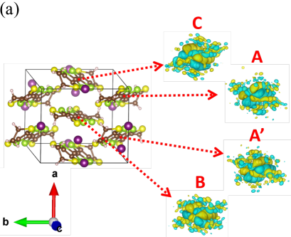
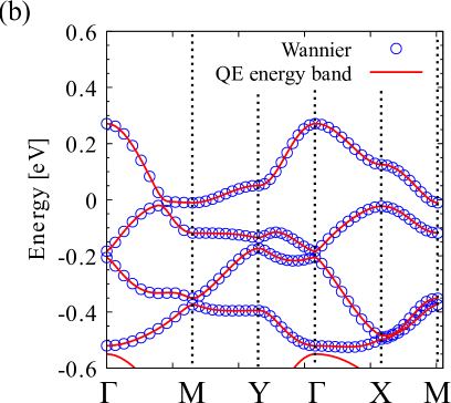
Figure 1(a) shows the crystal structure of -(BETS)2I3 at 30K under ambient pressure (left side) and the real space structure of the MLWFs at each site (right side). There are four BETS molecules labeled by A, A′, B, and C in the unit cell. They are distinguished by the arrangement and the orientation. A and A′ are crystallographically equivalent sites. The center positions of the MLWFs are located at the center of each BETS molecule, and as shown in Fig. 1(a), like orbitals are spreading in the direction perpendicular to the surface of the molecule. Figure 1(b) shows the energy bands near the Fermi energy (the energy origin is set as the Fermi energy) obtained by QE and the Wannier interpolation.
Next, we constructed the effective model using the transfer integrals and the on-site Coulomb interactions. The on-site Coulomb interactions are evaluated by the constrained random phase approximation (cRPA) method using RESPACK. The energy cutoff for the dielectric function was set as 5.0 Ry.
 List of transfer integrals obtained from MLWFs.
Re [meV]
(-1, 0)
A
B
158.7 ()
(0, 0)
A′
B
158.6 ()
(0, -1)
A′
C
138.1 ()
(-1, 0)
A
C
138.0 ()
(0, 0)
A
B
65.84 ()
(-1, 0)
A′
B
65.75 ()
(0, 0)
A
A′
51.08 ()
(0, -1)
C
C
21.92 ()
(-1,-1)
A′
C
18.65 ()
(0, 0)
A
C
18.48 ()
(0, -1)
A′
A
-16.31 ()
(0, -1)
A′
A′
14.24 ()
(0, -1)
A
A
14.19 ()
(0, -1)
B
C
10.12 ()
(0, 0)
B
C
9.864 ()
(-1,-1)
A′
A
9.212
(0, -1)
A′
B
6.737
(1, -1)
B
A
6.600
(1, -1)
B
C
5.065
(-1, 0)
B
C
5.010
List of transfer integrals obtained from MLWFs.
Re [meV]
(-1, 0)
A
B
158.7 ()
(0, 0)
A′
B
158.6 ()
(0, -1)
A′
C
138.1 ()
(-1, 0)
A
C
138.0 ()
(0, 0)
A
B
65.84 ()
(-1, 0)
A′
B
65.75 ()
(0, 0)
A
A′
51.08 ()
(0, -1)
C
C
21.92 ()
(-1,-1)
A′
C
18.65 ()
(0, 0)
A
C
18.48 ()
(0, -1)
A′
A
-16.31 ()
(0, -1)
A′
A′
14.24 ()
(0, -1)
A
A
14.19 ()
(0, -1)
B
C
10.12 ()
(0, 0)
B
C
9.864 ()
(-1,-1)
A′
A
9.212
(0, -1)
A′
B
6.737
(1, -1)
B
A
6.600
(1, -1)
B
C
5.065
(-1, 0)
B
C
5.010
|
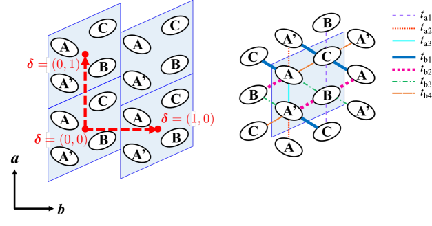
Figure 2 shows a schematic lattice structure of -(BETS)2I3. The transfer integrals are considered up to almost the next nearest neighbor bonds (shown in the center figure and table of Fig. 2). The values of the transfer integrals are listed in the table shown in the right side of Fig. 2. Here, indicates the relative lattice vector and and indicate the site indexes in the unit cell, i.e., A, A’, B, and C. The cutoff energy of the transfer integrals are taken as [meV]. The on-site Coulomb interactions are given as [eV], [eV], and [eV]. Since the transfer integrals between the inter planes are significantly smaller than those in the intra plane [42], this system can be considered as a two-dimensional electron system.
In this study, we investigated the two-dimensional Hubbard model with SOI [43, 44]:
| (1) | |||||
where is the coordinate of the unit cell, and , indicate the indexes of the inner-sites in the unit cell (A, A′, B, and C). indicates the index of spin. indicates the transfer integral between and sites separated by the relative lattice vector , and indicates the on-site Coulomb interaction evaluated using cRPA method. Here, the site potentials are [eV], [eV], and [eV]. We ignored these terms in eq. (1) because their contribution to the energy band obtained in our model is insignificant. The creation (annihilation) operator at -site in the unit cell located at is defined as (), and the number operator is defined as . () is a tuning parameter that controls the values of the on-site Coulomb interaction. is the SOI term, which is generally proportional to , where is the momentum, is the potential energy, and indicates the spin angular momentum. The specific formula of is detailed in the following section. The fourth term of Eq. (1) represents the in-plane Zeeman magnetic field, where is the Bohr magneton. In the following, the lattice constants, Boltzmann constant , and the Plank constant are taken as unity. Note that electronvolt (eV) is used as the unit of energy throughout this paper.
II.2 Electronic state in the wavenumber space
In this study, we investigate the electronic state using the Hartree approximation. To obtain the Hamiltonian in the wavenumber representation, the Fourier inverse transformation is performed on the Hamiltonian defined in Eq. (1). Then, the Hamiltonian is given as
| (2) | |||||
where indicates the wavenumber vector. Here, is the Hamiltonian of the SOI and is given as the following formulas [45]:
where the spin and is the control parameter of the strength of the SOI.
is diagonalized by using the eigenvector about each , and the energy eigenvalues () are obtained. In the following, for convenience, we define as
| (3) |
where the chemical potential is determined to satisfy the -filling. The charge density for site and spin is calculated as using the Fermi distribution function . The Berry curvature in band and spin is obtained by
| (4) |
where
| (5) |
and the Chern number is given as .
| (6) |
Here, indicates that the integration is performed throughout the Brillouin zone.
II.3 Conductivity
The optical conductivity in the clean limit is calculated using the Nakano-Kubo formula [33, 13, 34, 35, 36] given as follows
| (7) | |||||
| (8) | |||||
| (9) |
where and the angle is measured from the -axis direction and the projection in the -direction of the velocity indicating the inter-band transition written as
| (10) |
Here, is defined as
| (11) | |||||
In the limit of in Eq. (7), the DC conductivity is represented by the following equations:
| (12) | |||||
| (13) | |||||
where the relaxation time is calculated within the -matrix approximation using the perturbation theory for the green function. We only treat an elastic scattering between electrons and impurities, which is originated from a lack and disorder of anion I molecules. The impurity potential term is considered as
| (14) |
where is the intensity of the impurity potential and is the coordinate of impurities. The imaginary part of the retarded self-energy gives the damping constant and the is obtained as follows.
| (15) | |||||
Here, is the density of impurities and
indicates the total density of states. In the following, the unit of conductivity is the universal conductivity , and the Drude term is subtracted from the optical conductivity.
III Numerical Results
III.1 Electronic state at finite temperature
In this subsection, the electronic state at a finite is investigated under the condition of .
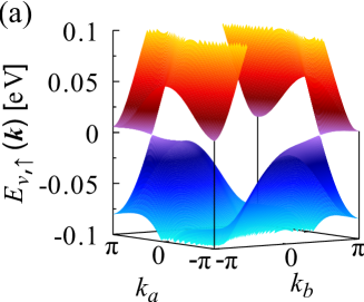
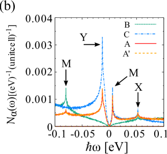
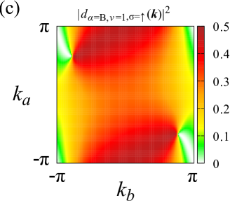
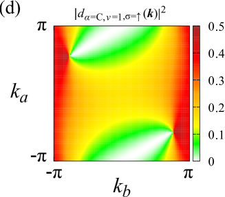
Figure 3(a) shows the energy eigenvalues near the Fermi energy calculated using the tight-binding model (). The conduction band () and valence band () form the Dirac point, and a type-I Dirac electron system that appears in the high-pressure phase of -(BEDT-TTF)2I3 is expected to be realized under ambient pressure in -(BETS)2I3.
Figure 3 (b) displays the density of states in the energy range . The order of magnitudes near the Fermi energy (approximately ) is . The presence or absence of peaks of the van Hove singularity at each site is related to the property of the eigenvector . Note that the lines of and has the same value due to the inversion symmetry and overlap each other. Figure 3(c) and (d) show the square of the absolute value of the eigenvector in B and C, respectively. The zero line appears in , which has almost the same wavenumber dependence as -(BEDT-TTF)2I3 [46]. Accordingly, the electronic state of -(BETS)2I3 in the high- phase under ambient pressure is similar to this, as demonstrated by -(BEDT-TTF)2I3 in the high-pressure phase.
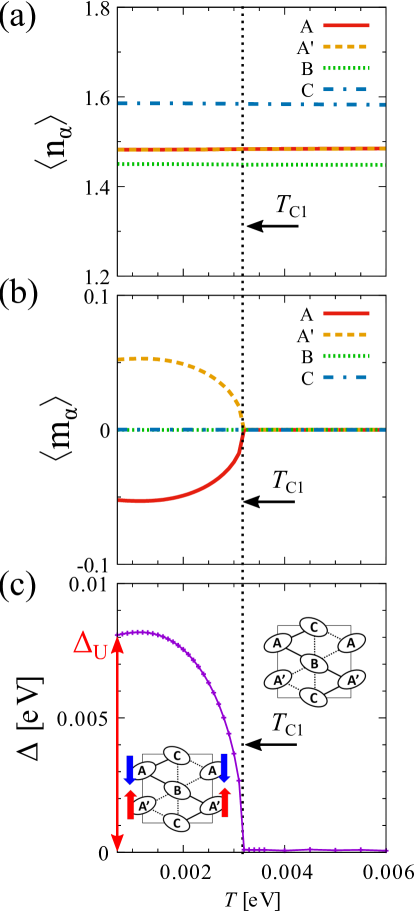
Hereafter, we fixed as , so that the phase transition matches to that observed in the experiments and investigated the effects of the on-site Coulomb interaction within the Hartree approximation. Figure 4(a) and (b) show the -dependence of the charge density and magnetization density at each site in the unit cell. It is observed that with decreasing from , the charge densities hardly change, whereas the spin densities at A and A′ sites change rapidly at the temperature . Here, and have different values owing to the charge disproportionation originated from the anisotropy of transfer integrals and it is not related to the charge order. These results indicate that the system does not break the charge inversion symmetry, but breaks the spin inversion symmetry below . Such a magnetic phase transition has not been observed so far, but the divergent increase of spin susceptibility associated with this spin order in is probably canceled out due to the nature of the wave function in Dirac electron systems. In the previous theoretical study [43, 44], antiferromagnetism in the unit cell with vertical-stripe charge order was pointed out. However, the structure analysis in the experiments shows that the charge inversion symmetry is not broken and charge density at each site is hardly changed as is decreased [27]. This fact is consistent with our results. The remainder of this paper, we theoretically investigate the anomalous competitive effect with and SOI whether magnetic transition actually occurs or not, when such a spin order exists in -(BETS)2I3. Figure 4(c) shows the -dependence of the energy gap . has a finite value at owing to the occurrence of the spin-order phase transition.
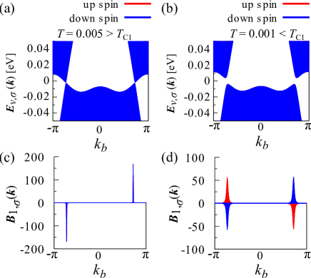
Figure 5(a) and (b) show the energy bands at and , respectively. In the spin-ordered state, opens at the Dirac point, but the spin components of the energy bands do not split. On the other hand, Figs. 5(c) and (d) show the Berry curvatures at and . As shown in Fig. 5(c) and (d), the sign of inverts according to the degrees of freedom about spin and valley indices , where the right (left) Dirac cone corresponds to , respectively. Therefore, when such a spin-ordered massive Dirac electron (SMD) phase exists, it is expected that a unique spin-valley Hall effect appears. The intrinsic and side-jump terms of the valley-spin Hall conductivity on -th band can be written in the form of
and
where is the energy band at the wavenumber around the left or right Dirac point [47, 48, 49]. The Hall conductivity is defined by . The spin and valley Hall conductivities are calculated by and , respectively. Subsequently, the spin-valley Hall conductivity is obtained by and this value becomes finite in the SMD phase. It is expected that the spin (valley) Hall effect depending on the degrees of freedom about valley (spin) appears [50].
III.2 Effects of SOI on the electronic state
In this subsection, the contribution of SOI to the electronic state at a finite is examined. When only SOI is considered, i.e., , a metallic band appears owing to the edge state, as shown in Appendix A. In this case, the insulating behavior at low of -(BETS)2I3 cannot be explained. In the following, we investigate the effects of SOI in the presence of on-site Coulomb interactions . For simplicity, we set and as in the previous subsection.
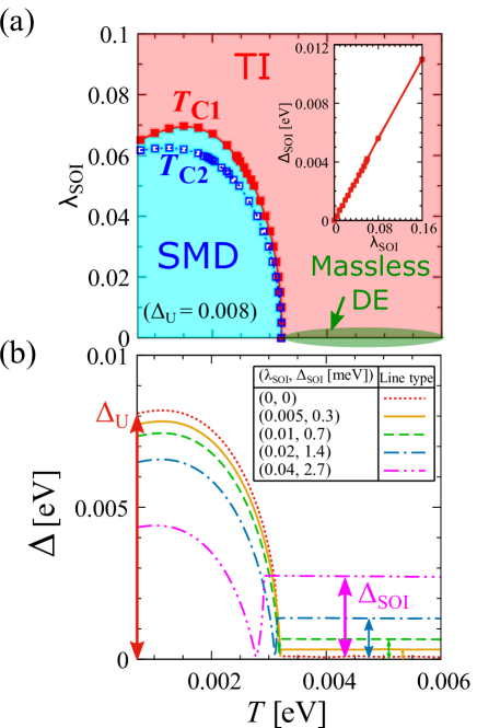
Figure 6(a) and (b) show the phase diagram and the -dependence of the energy gap at several values, respectively. Note that the value of the transfer integrals has the order of eV (see Fig. 2), therefore, the magnitude of the SOI for is approximately 1 meV. Hereinafter, for convenience, we introduce two energy scales: SMD gap and SOI gap . is defined as the value of the energy gap at for (red solid arrow in Fig. 4(c) and Fig. 6(b)). is the value of in which is associated with the energy scale of the SOI (magenta to orange solid arrows in Fig. 6(b)). The inset of Fig. 6(a) shows the -dependence of the SOI gap at . When and , the value of is finite, and the system becomes a topological insulator (TI) as described below. It should be noted that for (), exhibits a -shaped -dependence at ; i.e., decreases to zero in , becomes zero at , and is finite again in . As () is increased, gradually decreases and reaches to zero. The SMD phase vanishes in () and a quantum phase transition can occur when such a large SOI exists. However, this value is more than twice the SOI value estimated by first-principles calculation [32].
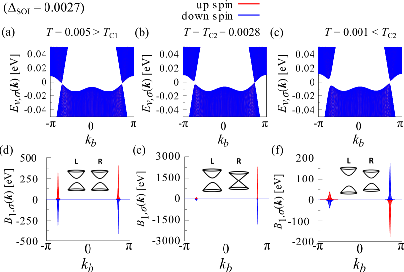
Figure 7 shows the energy band near the Fermi energy and Berry curvature at () in the following three cases: [Figs. 7(a) and (d)], [Figs. 7(b) and (e)], and [Figs. 7(c) and (f)]. First, when , the time-reversal symmetry exists, and the SOI gap opens at the Dirac point [Fig. 7(a)]. In this case, the sign of is inverted according to the spin components, as illustrated in Fig. 7(d), and the system becomes the TI because the spin Chern number defined by becomes .
Thereafter, in [Figs. 7(b) and (e)], the time-reversal symmetry is broken. Hence, has peaks with different magnitudes according to the left and right valleys, and the spin Chern number has a real finite value. At , the sign of in one valley is inverted corresponding to at one valley. Finally, for , gaps of different sizes are opened [Fig. 7(c)]. These behaviors in originate from the competition between the contributions of the spin order and SOI [51, 52, 53, 54, 55, 56, 57, 58]. Moreover, as the sign of the in one valley has been already inverted at , the spin Chern number is zero in this region [Figs. 7(c) and (f)].
III.3 DC and optical conductivities
In this subsection, is fixed at 0.008 as in the previous section, and the and SOI effects on the DC and optical conductivities are investigated.
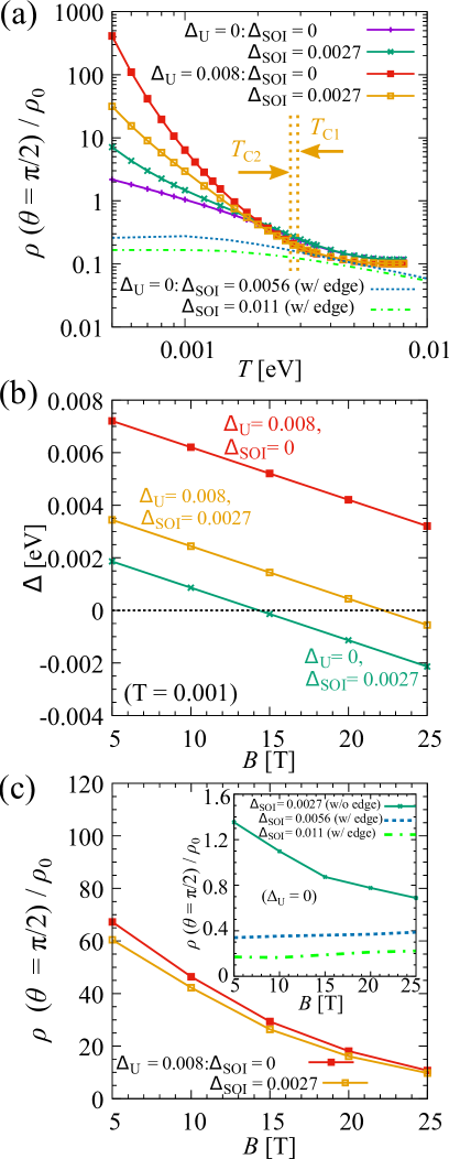
The -dependence of the -axial DC resistivity for , , , and is plotted in Fig. 8(a) as solid lines. When only the SOI is considered (), the system becomes the TI, in which the SOI gap is opened at the Dirac point and increases at quite low as is decreased. Moreover, when considering the on-site Coulomb interaction, increases below the phase transition temperature owing to the spin order gap. However, as a result of the finite energy width owing to and the gentle function, such as of the energy gap [see Eq.(12) and Fig. 4(c)], does not increase suddenly near the SMD phase transition temperature . When both the on-site Coulomb interaction and SOI are taken into account, the spin order gap is suppressed by the SOI. Thus, is suppressed at low .
Here, note that in Fig. 8(a), we also plot the -dependence of at (dashed line), and (dotted chain line) obtained by the calculation using the cylindrical boundary condition. When only the SOI exists in the system with edge, the helical edge state appears, and saturates, as shown by these lines. Owing to the edge conduction, the value of has no significant change even when we consider large SOI. Therefore, we cannot explain the divergent increase of the DC resistivity observed in the experiment of -(BETS)2I3 when considering the SOI alone, and the edge state is robust (See Appendix A for details).
Figures 8(b) and (c) represent the in-plane magnetic field -dependence of the energy gap and for several values of . The energy band is split by (see Eq. (1)). Thus, monotonically decreases as is increased when calculating without edges. As a result, in Fig. 8(c) and the solid line in its inset, decreases as is increased. This result is consistent with the negative magnetoresistance observed in -(BETS)2I3 [59]. However, when considering the edge in the system, as shown by the dashed line and dotted chain line in the inset, is almost constant, owing to the edge conduction. Hence, we can not explain the negative magnetoresistance when considering the SOI alone.
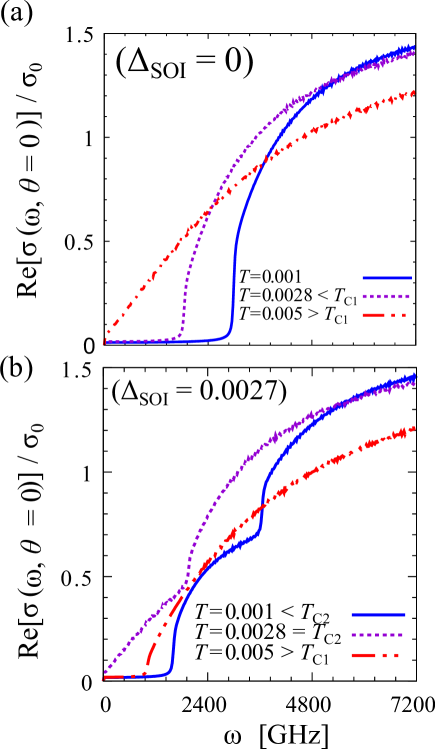
Figures 9(a) and (b) show the real part of the optical conductivity along the -axis () direction Re for and () around . Re shows clear differences depending on the presence or absence of the SOI. In , Re without the SOI has a finite value at frequency , whereas that with the SOI remains zero until reaches approximately 960 GHz because of the finite SOI gap. In , Re without the SOI becomes zero when the value of is smaller than the spin order gap , and increases abruptly in . However, when the SOI is considered, exhibits a V-shaped -dependence owing to the competition between the SMD and SOI, as indicated in Fig. 6(b). As a result, Re increases abruptly by two times corresponding to the different s in the left and right valleys. Furthermore, at , Re with the SOI has a finite value because in the right valley is closed.
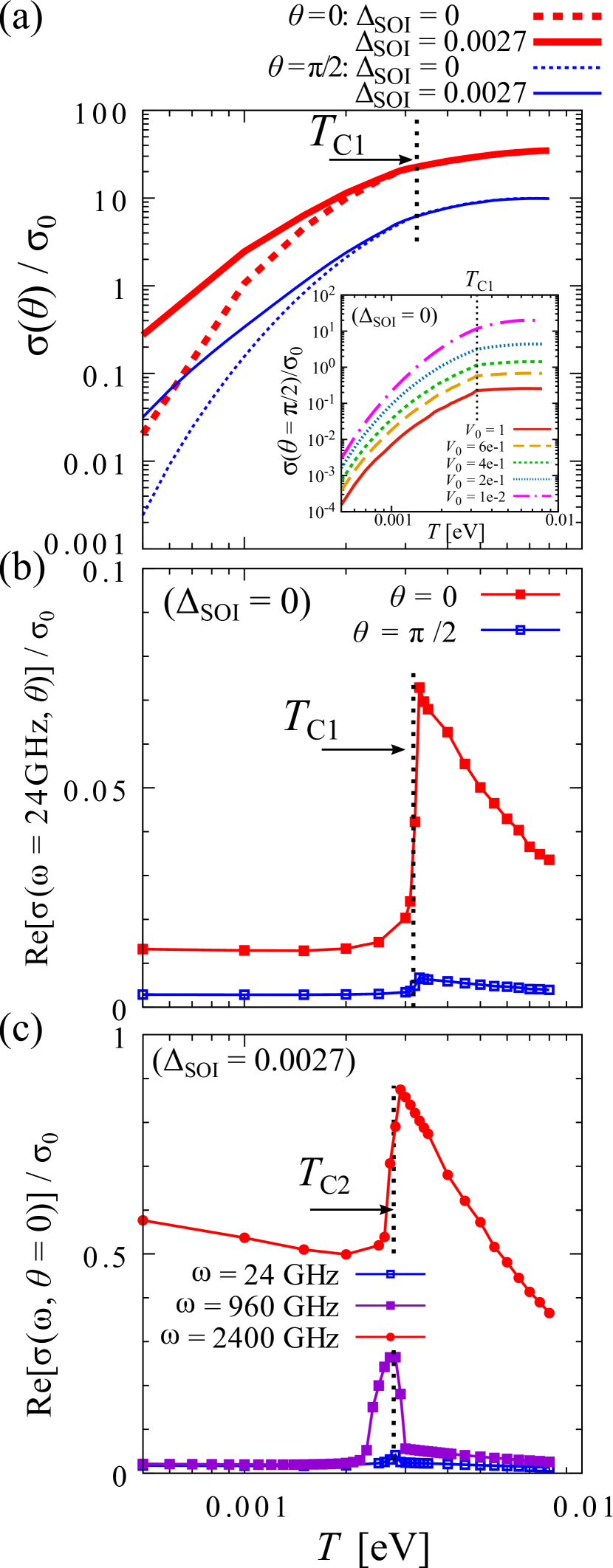
Figure 10(a) shows the -dependence of the DC conductivity along the -axis () and -axis () directions. decreases exponentially in , but a clear discontinuous jump does not appear at because is influenced by the energy width of , as indicated in Eq. (12). -dependence of at , for several values of the strength of impurity potential (see eq. (14)) are plotted in the inset of Fig. 10(a). The absolute value of increases as is decreased from to , but no discontinuous change appears at for any value when the conductivity is calculated based on eqs. (12)-(15). Figure 10(b) shows the real part of the optical conductivity Re in the absence of the SOI. As is decreased, in contrast to the DC conductivity, Re increases gradually towards and decreases suddenly in . The optical conductivity calculated by Eqs. (7) to (9) is considered as a direct transition in the inter-band at the same wavenumber and frequency . Therefore, when is finite in , the possible direct transition at the energy GHz eV disappears and Re decreases sharply. Finally, the -dependence of Re in the presence of the SOI for several frequencies is plotted in Fig. 10(c). Re with the SOI has a peak at , where the gap of the right valley is closed.
IV Summary and Discussion
In this study, first, a Hubbard model was constructed as an effective model in the two-dimensional conduction plane of -(BETS)2I3 based on the synchrotron X-ray diffraction data at 30K under ambient pressure. We investigated the effects of the on-site Coulomb interaction and SOI at a finite temperature within the Hartree and -matrix approximations to clarify the insulating behavior observed in -(BETS)2I3 in the low region.
We found the phase transition between the weak TI phase and SMD phase. In the SMD phase, the time-reversal symmetry is broken, but the spatial inversion and translational symmetries are conserved. The SMD phase is not a conventional spin-ordered state, but exhibits the physical properties that reflect the wave functions of Dirac electrons. It is expected that the spin-valley Hall effect occurs because the sign of the Berry curvature is reversed depending on the freedoms of the spin and valley. The SMD has the energy gap at the Dirac points, whereas the energy band in the bulk does not split in the spin degrees of freedom. The energy gaps of different sizes open in the left and right valleys owing to the competition between the SMD and SOI, as shown in the honeycomb lattice system in previous studies [51, 52, 53, 54, 55, 56, 57, 58]. Next, we calculated the - and -dependences of the DC resistivity. When considering the SOI alone and the system has edges, the helical edge state appears in the energy gap, and the DC resistivity saturates toward low . The negative magnetoresistance does not appear in this case. On the other hand, in the SMD phase, the DC resistivity increases divergently as is decreased, and there is no noticeable change near the SMD phase transition temperature . The DC resistivity exhibits the negative magnetoresistance, owing to the Zeeman split of the energy band. Finally, it was shown that the -dependence of the microwave (about eV) conductivity shows clear changes at the vicinity of .
In recent magnetoresistivity measurements, a positive magnetoresistance and a negative magnetoresistance were observed at K under in-plane and perpendicular magnetic fields, respectively. This is the characteristic of the two-dimensional Dirac electron system [59]. On the other hand, a negative magnetoresistance appeared at K under both in-plane and perpendicular magnetic fields [59]. Furthermore, it was also pointed out that at K, the Seebeck coefficient exhibits a nonmonotonic -dependence [59]. Those experimental results indicate that the electronic states change around 50 K. The TI-SMD transition shown in the present paper is consistent with the electric transport properties and the structure analysis observed in -(BETS)2I3 [25, 27, 59]. The existence of the TI-SMD transition can be directly confirmed by the microwave conductivity.
In the present study, the control parameter of SOI and spin are treated as constants for simplicity. When we only discuss the qualitative behavior, the results shown in the present study (e.g. difference of the size in energy gaps between two Dirac cones in , and TI phase in ) can be explained well in the range of this approximation and is robust for any other treatment of SOI because these behaviors are originated from the effects of on-site [51, 52, 53, 54, 55, 56, 57, 58]. Time reversal symmetry (TRS) is conserved in TI phase, but antiferromagnetism induced by breaks the TRS [55], and causes the different size of energy gap between the left and right cones. Therefore, main result in this study is due to the effect of , regardless of the detailed handling about SOI, so the approximation used in this study is sufficient to show the main results in our study. However, more exactly, it is necessary to treat and spin as vector quantities in consideration of the anisotropy of SOI [31] to have a quantitative discussion.
When the spin order such as SMD phase appears, a clear change is expected to appear in the spin susceptibility. In the NMR experiment for -(BETS)2I3 [26], no signs of magnetic transition have been observed near the insulating phase. However, clear changes in the physical quantities in NMR (Knight shift and ) originated from the SMD phase transition may be canceled out due to the nature of phase of the wave function in the Dirac electron systems. This behavior can also be shown in Dirac electron systems such as an anisotropic square lattice model [8]. The detailed analysis of the SMD phase and physical quantities of NMR in -(BETS)2I3 are currently in progress and will be reported in another paper. The nonmonotonic -dependence on the Seebeck coefficient of -(BETS)2I3 is also to be investigated in the future. When the time-reversal symmetry is broken by the SMD phase, the helical edge state due to the SOI is not protected, and the energy gap can open [60, 61, 62]. Transport properties in the presence of impurities on the edges are to be investigated in the SMD phase with the SOI.
The SMD phase is expected to be affected by the long-range Coulomb interaction and the spin fluctuation enhanced near the SMD phase transition. To treat these effects, the calculation using the extended Hubbard model and the vertex correction[63, 64] should be performed and remains as future problems.
Acknowledgements.
The authors would like to thank H. Sawa, T. Tsumuraya, and S. Kitou for valuable discussions and advices about the numerical calculation. We would also like to thank S. Onari, Y. Yamakawa, and H. Kontani for fruitful discussions. The computation in this work was conducted using the facilities of the Supercomputer Center, Institute for Solid State Physics, University of Tokyo. This work was supported by MEXT/JSPJ KAKENHI under grant numbers 19J20677, 19H01846, and 15K05166.Appendix A Electrical resistivity if only spin-orbit interaction is considered
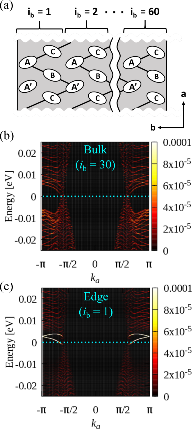
In this appendix, we show the results of the analysis of the DC resistivity of -(BETS)2I3 when only the SOI is considered. To investigate the effects of the edge state on the DC resistivity, we impose the cylindrical boundary condition on the system, as illustrated in Fig. A.1(a), and consider the term of SOI introduced in the main text and Ref [45]. The Fourier inverse transform is performed in the -axial direction and represented by the wavenumber , whereas the real space structure in the -axial direction is labeled by the coordinates of the unit cell . The system size along the -axis is set to , as illustrated in Fig. A.1(a), and thus, the Hamiltonian becomes a Hermitian matrix about each spin, which includes the information of the sublattice (A, A′, B, and C) and the unit cell coordinate ().
As a result of the numerical diagonalization, we obtain 240 energy eigenvalues () and the unitary matrix . Here, we introduce the spectral weight in each unit cell defined as
| (16) | |||||
Figures A.1(b) and (c) describe the for (bulk) and (left edge) for the parameters of (when considering the SOI alone). Although in Fig. A.1(b) is spread weakly over the whole energy range, is quite large near the Fermi energy, as shown in Fig. A.1(c), owing to the existence of a helical edge state protected by the time-reversal symmetry in the system. Therefore, the conduction channel of this edge state becomes dominant at .
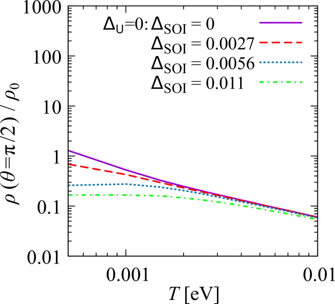
Figure A.2 shows the -dependence of the DC resistivity for , , , and . When the SOI is considered in the bulk, as calculated in the main text, the energy gap opens at the Dirac point, and the system becomes an insulator. However, when considering the SOI in a system with edges, the helical edge state appears in the vicinity of the Fermi energy owing to the band crossing between the up and down spin bands, so that it does not actually become an insulator. Note that the slight increase in the resistivity at near the lowest results from the energy gap associated with the finite-size effect. The edge state caused by SOI is topologically protected. On the other hand, edge state which is not protected and depends on the edge setting also appears in some cases. For instance, in the -type organic conductors, it is suggested that when the edge setting is symmetric, the edge state appears in the gapless band[36, 21]. Therefore, when such an edge state exists and the spin order by occurs, it is expected that the edge state associated with the AF at the edge appears in the gapless band and edge conduction occurs.
References
- [1] P. R. Wallace, Phys. Rev. 71 622 (1947).
- [2] K. S. Novoselov, A. K. Geim, S. V. Morozov, D. Jiang, M. I. Katsnelson, I. V. Grigorieva, S. V. Dubonos, and A. A. Firsov Nature 438 197 (2005).
- [3] P. A. Wolff, J. Phys. Chem. Solids 25 1057 (1964).
- [4] H. Fukuyama and R. Kubo, J. Phys. Soc. Jpn. 28 570 (1970).
- [5] K. Kajita, T. Ojiro, H. Fujii, Y. Nishio, H. Kobayashi, A. Kobayashi, and R. Kato, J. Phys. Soc. Jpn. 61, 23 (1992).
- [6] N. Tajima, M. Tamura, Y. Nishio, K. Kajita, and Y. Iye, J. Phys. Soc. Jpn. 69, 543 (2000).
- [7] A. Kobayashi, S. Katayama, K. Noguchi, and Y. Suzumura, J. Phys. Soc. Jpn. 73, 3135 (2004).
- [8] S. Katayama, A. Kobayashi, and Y. Suzumura, J. Phys. Soc. Jpn. 75, 054705 (2006).
- [9] A. Kobayashi, S. Katayama, Y. Suzumura, and H. Fukuyama, J. Phys. Soc. Jpn. 76, 034711 (2007).
- [10] M. O. Goerbig, J.-N. Fuchs, G. Montambaux, and F. Pichon, Phys. Rev. B 78, 045415 (2008).
- [11] K. Kajita, Y. Nishio, N. Tajima, Y. Suzumura, and A. Kobayashi, J. Phys. Soc. Jpn. 83, 072002 (2014).
- [12] N. Tajima, S. Sugawara, M. Tamura, Y. Nishio, and K. Kajita, J. Phys. Soc. Jpn. 75, 051010 (2006).
- [13] N. H. Shon and T. Ando, J. Phys. Soc. Jpn. 67 2421 (1998).
- [14] H. Seo, J. Phys. Soc. Jpn. 69, 805 (2000).
- [15] T. Takahashi, Synth. Met. 133-134, 26 (2003).
- [16] T. Kakiuchi, Y. Wakabayashi, H. Sawa, T. Takahashi, and T. Nakamura, J. Phys. Soc. Jpn. 76, 113702 (2007).
- [17] Y. Tanaka and M. Ogata, JPSJ 85, 104706 (2016).
- [18] K. Ishikawa, M. Hirata, D. Liu, K. Miyagawa, M. Tamura, and K. Kanoda, Phys. Rev. B 94, 085154 (2016).
- [19] R. Beyer, A. Dengl, T. Peterseim, S. Wackerow, T. Ivek, A. V. Pronin, D. Schweitzer, and M. Dressel, Phys. Rev. B 93, 195116 (2016).
- [20] D. Liu, K. Ishikawa, R. Takehara, K. Miyagawa, M. Tamura, and K. Kanoda, Phys. Rev. Lett. 116, 226401 (2016).
- [21] D. Ohki, Y. Omori, and A. Kobayashi, Phys. Rev. B 100, 075206 (2019).
- [22] M. Hirata, K. Ishikawa, K. Miyagawa, M. Tamura, C. Berthier, D. Basko, A. Kobayashi, G. Matsuno, and K. Kanoda, Nat. Commun. 7, 12666 (2016).
- [23] G. Matsuno and A. Kobayashi, J. Phys. Soc. Jpn. 87, 054706 (2018).
- [24] M. Hirata, K. Ishikawa, G. Matsuno, A. Kobayashi, K. Miyagawa, M. Tamura, C. Berthier, and K. Kanoda, Science 358, 1403 (2017).
- [25] M. Inokuchi, H. Tajima, A. Kobayashi, T. Ohta, H. Kuroda, R. Kato, T. Naito, and H. Kobayashi, Bull. Chem. Soc. Jpn. 68, 547 (1995).
- [26] K. Hiraki, S. Harada, K. Arai, Y. Takano, T. Takahashi, N. Tajima, R. Kato, and T. Naito, J. Phys. Soc. Jpn. 80, 014715 (2011).
- [27] S. Kitou, T. Tsumuraya, H. Sawahata, F. Ishii, K. Hiraki, T. Nakamura, N. Katayama, and H. Sawa, arXiv:2006.08978 [cond-mat.str-el] (2020).
- [28] R. Kondo, S. Kagoshima, N. Tajima, and R. Kato, J. Phys. Soc. Jpn. 78, 114714 (2009).
- [29] P. Alemany, J. P. Pouget, and E. Canadell, Phys. Rev. B 85, 195118 (2012).
- [30] T. Morinari and Y. Suzumura, J. Phys. Soc. Jpn. 83, 094701 (2014).
- [31] S. M. Winter, K. Riedl, and R. Valenti, Phys. Rev. B 95, 060404(R) (2017).
- [32] T. Tsumuraya, Y. Suzumura, arXiv:2006.11455 [cond-mat.str-el] (2020).
- [33] P. Steda and L. Smrka, Phys. Stattus Solidi B 70, 537 (1975).
- [34] I. Proskurin, M. Ogata, and Y. Suzumura, Phys. Rev. B 91 195413 (2015).
- [35] A. Regg, S. Pilgram, and M. Sigrist, Phys. Rev. B 77 245118 (2008).
- [36] Y. Omori, G. Matsuno, A. Kobayashi, J. Phys. Soc. Jpn. 86, 074708 (2017).
- [37] P. Giannozzi, S. Baroni, N. Bonini, M. Calandra, R. Car, C. Cavazzoni, D. Ceresoli, G. L Chiarotti, M. Cococcioni, I. Dabo, A. Dal Corso, S. de Gironcoli, S. Fabris, G. Fratesi, R. Gebauer, U. Gerstmann, C. Gougoussis, A. Kokalj, M. Lazzeri, L. Martin-Samos, N. Marzari, F. Mauri, R. Mazzarello, S. Paolini, A. Pasquarello, L. Paulatto, C. Sbraccia, S. Scandolo, G. Sclauzero, A. P Seitsonen, A. Smogunov, P. Umari and R. M Wentzcovitch, J.Phys.: Condens. Matter 21, 395502 (2009).
- [38] J. P. Perdew, K. Burke, and M. Ernzerhof, Phys. Rev. Lett. 77, 3865 (1996).
- [39] M. Schlipf and F. Gygi, Computer Physics Communications 196, 36 (2015).
- [40] K. Nakamura, Y. Yoshimoto, Y. Nomura, T. Tadano, M. Kawamura, T. Kosugi, K. Yoshimi, T. Misawa, and Y. Motoyama, arXiv:2001.02351v1 [cond-mat.str-el] (2020).
- [41] K. Momma and F. Izumi, J. Appl. Cryst. 44, 1272-1276 (2011).
- [42] Transfer integrals to the neighboring plane are all on the order of 0.1 [meV] [meV].
- [43] H. Kino and H. Fukuyama, J. Phys. Soc. Jpn. 64, 1877 (1995).
- [44] H. Kino and H. Fukuyama, J. Phys. Soc. Jpn. 65, 2158 (1996).
- [45] T. Osada, J. Phys. Soc. Jpn. 87, 075002 (2018).
- [46] A. Kobayashi and Y. Suzumura, J. Phys. Soc. Jpn. 82, 054715 (2013).
- [47] S. Murakami, N. Nagaosa and S.C. Zhang, Science 301, 1348-1351 (2003).
- [48] D. Xiao, W. Yao, and Q. Niu, Phys. Rev. Lett. 99, 236809 (2007).
- [49] G. Matsuno, Y. Omori, T. Eguchi, and A. Kobayashi: J. Phys. Soc. Jpn. 85 094710 (2016).
- [50] D. Xiao, G. B. Liu, W. Feng, X. Xu, and W. Yao, Phys. Rev. Lett. 108, 196802 (2012).
- [51] M. Ezawa, J. Phys. Soc. Jpn. 84, 121003 (2015).
- [52] R. S. K. Mong, A. M. Essin, and J. E. Moore, Phys. Rev. B 81, 245209 (2010).
- [53] D. Zheng, G. M. Zhang, and C. Wu, Phys. Rev. B 84, 205121 (2011).
- [54] S. Miyakoshi and Y. Ohta, Phys. Rev. B 87, 195133 (2013).
- [55] J. Cao and S. Xiong, Phys. Rev. B 88, 085409 (2013).
- [56] M. Hohenadler, F. Parisen Toldin, I. F. Herbut, and F. F. Assaad. Phys. Rev. B 90, 085146 (2014).
- [57] A. Sekine and K. Nomura. Phys. Rev. Lett. 116, 096401 (2016).
- [58] K. Jiang, S. Zhou, X. Dai, and Z. Wang. Phys. Rev. Lett. 120, 157205 (2018).
- [59] N. Tajima (2019, private communication).
- [60] R. R. Biswas, and A. V. Balatsky, Phys. Rev. B 81, 233405 (2010).
- [61] C. Fang, M. J. Gilbert, and B. A. Bernevig, Phys. Rev. B 88 085406 (2013).
- [62] Y. Tokura, K. Yasuda, and A. Tsukazaki, Nat. Rev. Phys. 1, 126 (2019).
- [63] K. Yoshimi, H. Maebashi, and T. Kato, J. Phys. Soc. Jpn. 78, 104002 (2009).
- [64] S. Raghu, X. L. Qi, C. Honerkamp, and S. C. Zhang, Phys. Rev. Lett. 100, 156401 (2008).