The impact of metallic contacts on spin-polarized photocurrents in topological insulator nanowires
Abstract
Recently, a quantum phase, the topological insulator, has been vividly investigated in a variety of materials. Its unique bandstructure allows for optical generation and control of spin-polarized currents based on the circular photogalvanic effect. In this paper, we generate and distinguish the different photocurrent contributions via the polarization of the driving light wave. We discuss the helicity-dependent spin-polarized current and the polarization-independent thermoelectric current as spatially resolved maps, focusing on the influence of the topological insulator/metallic contact interface. We observe for both current contributions a significant enhancement of the current values at the topological insulator/metallic contact interface. In the case of the thermoelectric current the enhancement is localized at the center of the interface. The spin-polarized current reaches two extrema per contact, which differ by their sign and are localized nearby the contact edges. We discuss the general behavior of the thermovoltage as a three-material Seebeck effect and explain the enhanced values by the acceleration of the photoelectrons generated in the space charge region of the topological insulator/metallic contact interface. Furthermore, we interpret the temperature gradient together with the spin Nernst effect as a possible origin for the enhancement and spatial distribution of the spin-polarized current.
Recently, topological order gained a lot of attention among physicists after the discovery of topological insulators (TIs) [1, 2, 3] in solid state materials. This additional state of quantum matter differs from trivial insulators by hosting a bulk energy gap, while the surface possesses gapless electronic states. The nanowires investigated in this paper consist of . This material is a three-dimensional topological insulator with time-reversal symmetry[4, 5]. Thus, the surface states of are helical and the spin degeneracy is lifted at the surface. Also the backscattering of the surface electrons is suppressed [6, 7]. Those three properties make a promising candidate for spintronics- or optoelectronics applications.
The surface states make those materials suitable for polarization-sensitive detectors based on the polarization-dependent photovoltaic or photogalvanic effects [8, 9]. Both effects are based on creating an asymmetric population of the spin-polarized surface states. Since the momentum and spin orientation are locked at the surface, the asymmetry in the surface state population generates a spin-polarized electrical current. When the asymmetry is generated by exciting the surface states with circular-polarized light, the effect is known as the circular photogalvanic effect (CPGE) [10]. The CPGE has been observed in several optoelectronic experiments, which demonstrate the direction control of spin-polarized currents by circular-polarized light in TI materials [11, 12, 13]. The dimensions of those investigated TIs are in the micrometer range. Little is known about those effects when the dimensions of TIs decrease towards the nanometer scale e.g. in nanowires. There is one example for all-optical control in nanowires by Seifert et al.[13]. They observe an enhancement of the THz amplitude in the vicinity of the gold contacts which they explain by a locally enhanced spin-polarized current. In a previous work we measured the polarization-dependent photocurrent while scanning the nanowire [14]. We observed that the polarization-independent current contribution is dominated by the Seebeck effect. We also detect a helicity-dependent current contribution caused by the CPGE. In both cases, we observed that the values of the contributions increase in the vicinity of the gold contacts, but we did not discuss the origin in detail. In this paper, we explicitly discuss the influence of the metallic contacts on the thermoelectric and spin-polarized current. We generate the two-dimensional scans for both contributions to discuss the origin of their enhancement close to the topological insulator/metallic contact interface.
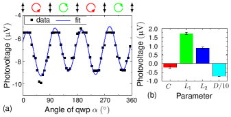
The photoelectric measurements in this paper are performed on nanowires synthesized by the gold-catalyzed vapor-liquid-solid method (for more details on the nanowire growth see Shin et al. [15]). The nanowires are grown in [110] direction as single-crystal structures assuring a smooth surface. The nanowire width is in the order of and the thickness spans from to , thus hybridization of the topological surfaces states can be excluded [16, 15]. The nanowires are transferred mechanically to a Si(111) substrate with of . The contact pads of Cr underneath Au are patterned on top of the nanowire with a spacing of . The photoelectric measurements are recorded using a well established lock-in technique. The light source is a diode laser with a wavelength of () modulated at by a square-function generator. The laser beam is guided through a linear polarizer combined with a rotatable quarter-wave plate (qwp) for polarization control before impinging at an angle of incidence of on the sample surface. The laser light is focused down to a spot size of on the sample surface. The measured photocurrent (photovoltage ) is mapped to the polarization state via the qwp rotational angle . Thus, the photocurrent is measured at fixed positions (k,j) for linear, left-circular and right-circular polarized light, scanning the sample surface vertically and horizontally by moving the laser across the sample surface with stepper motors. At the same time, the light intensity reflected from the sample surface is recorded by a second lock-in amplifier via a photodiode. The qwp rotates at every laser spot position (k,j) from with a step size of . Afterwards, the laser spot is moved in the vertical direction by to the next position . There, the photocurrent and the reflected intensity are measured again for a full qwp rotation. This generates a set of 60 current (voltage) values at each position (j,k) as presented in FIG. 1(a).
The data is evaluated by identifying the contributions in the measured photocurrent (voltage) by their polarization dependence. We use the ansatz suggested by McIver et al. [11] that includes four contributions:
| (1) |
In our measurements, the laser light is linear polarized at , left-circular polarized at and right-circular polarized at . The term in Eq.(1) represents the spin-polarized helicity-dependent current. The amplitude is the photocurrent difference between - and -light. The qwp phase is set so that is zero for linear polarized light. The physical origin of this term is still under discussion. Measurements by Shalygin et al. on (110)-grown GaAs/AlGaAs quantum wells prove that the circular photon drag effect can cause a helicity-dependent current [17], while later measurements on exfoliated Hall bar devices by McIver et al.[11] relate the helicity-dependent currents to the CPGE. The lifted spin degeneracy of surface electrons in a TI enables to generate an asymmetrical population of the spin-polarized surface states in the k-space by circular polarized light, since the optical selection rules for interband transitions have to be fulfilled. The asymmetric populated surface states cause an electrical spin-polarized current, since the spin and its momentum are locked on the surface of a TI. That exciting the spin-polarized surface states optically can lead to spin-polarized photocurrents has among others been demonstrated by Takeno et al. [18] by performing time-domain terahertz wave measurements and time-resolved magneto-optical Kerr rotation measurements. Hence, it is possible to generate a measurable helicity-dependent photocurrent due to the CPGE, which is spin-polarized [10, 12, 19, 20, 21, 13]. Therefore, we relate the first term in Eq. (1) to the CPGE following the notation established in the recent works [11, 22] and discuss the amount of spin-polarized current by displaying the amplitude .
The second term and third term in Eq. (1), have a different frequency than the first term. Thus, they do not affect the first term. The third term represents the polarization-dependent absorption. The physical effects related to the two contributions are still under discussion both being sometimes related to the linear photogalvanic effect or the photon drag effect [11, 23, 24]. The last term is polarization-independent and can originate from the polarization-independent photogalvanic effect, the photon drag effect and, due to the laser light heating, the Seebeck effect. We observed in a previous work ref. [14], that the contributions of the polarization-independent photogalvanic and photon drag effect to the over all behavior of D seem to be small compared to the contribution of the Seebeck effect.
For data analysis, the function () is fitted to the experimental data to extract the parameters , , and at each position as in FIG. 1(a). The values for the four parameters and their uncertainties are displayed in FIG. 1(b). The parameters and are displayed in two dimensional maps as a function of the laser spot position, see FIG. 2(b) and (c). The contact pad positions (edges are marked by orange lines) and the nanowire (black line) are determined from the reflectivity data and are in good agreement with the microscope images of the area of interest (see FIG. 2(a) and FIG. 3(c) and (f)). In the following we concentrate on the parameters and to investigate the influence of the thermoelectric current on the spin-polarized photocurrent and their enhancement in the vicinity of the contact pads.
The two-dimensional map of the parameter D in FIG. 2(b) shows that the thermocurrent reaches the largest values at the crossing of the nanowire and the contacts. This is visible in the contour plots in gray and pink in FIG. 2(b). The contour plot (green line in FIG. 2(b)) along the nanowire demonstrates that the increase is located at the metal contacts. Between the contacts the thermocurrent changes it sign and the slope of the thermocurrent is small, just like in ref. [14]. When the laser partly illuminates the crossing of the nanowire and metal contact, the thermocurrent increases drastically until it reaches its largest value at a horizontal position of . The origin of this enhancement is discussed later in the manuscript.
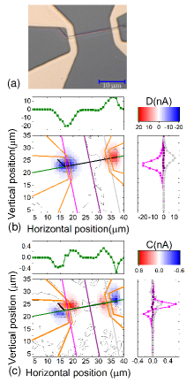
The current map of the spin-polarized current, represented by the parameter C, is displayed in FIG. 2(c). C is constant in the middle of the nanowire where the contact pads can be neglected and thus the transport is entirely determined by the surface states. This matches prior research [14]. When the laser spot illuminates the nanowire close to the contact pads, the spin-polarized current increases and reaches its extremal values nearby the contact edges.
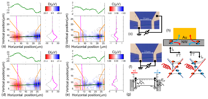
The measurement was repeated on a second nanowire, maintaining the contact distance and laser conditions, but changing the contact geometry. The results for axisymmetric contacts or point-symmetric contacts are shown in FIG. 3. For the thermoelectric contribution, we observe for both contact geometries enhanced values at the crossing of the contacts and the nanowire. The thermovoltage in FIG. 3(a) reaches at the drain electrode and goes down to at position (12,7) on the nanowire, which qualitatively matches the findings for the thermoelectric current in FIG. 2. In FIG. 3(b) and (e), the voltage C generated by the spin-polarized current for the two contact geometries are displayed. The voltage C reaches a minimum of at (22,8) close to the source electrode and decreases to at (14,8) at the nanowire center. Nearby the crossing of the contact pad and the nanowire, the voltage C reaches its extrema, which is in good agreement with the results observed in FIG. 2(c). Switching between the axisymmteric and the point-symmetric contacts does not affect the shape of the distribution or the sign of the voltage C at different areas (see FIG. 3(b) and (e)).
The two-interface Seebeck effect discussed in the supplemental material explains why the thermovoltage depends linear on the laser spot position. Thus, the two-interface Seebeck effect in the supplemental material explains the linear region of the contour plot in FIG. 3(a) and (d) but not the enhancement of the thermovoltage at the metal contacts. Hence, an additional effect is needed to explain the thermovoltage enhancement at the nanowire/contact interface. The band gap of is which is typical for semiconductors. Therefore, we expect a band bending at the interface as sketched in FIG. 3(g). Due to the band bending, a positive (negative) space charge zone forms at the contact (nanowire) at the interface. When the laser illuminates the nanowire underneath the drain electrode, an electron-hole pair is created. The electron will be accelerated to the drain electrode and the hole to the center of the nanowire, driven by the electric field around the interface. The electrons entering the drain electrode will contribute to the net-positive current when the holes annihilate with electrons, originating from the source electrode. The photoelectrons generated close to the source electrode contribute to the net-negative current, since the electric field of the space charge region changes it sign. The enhancement at the drain electrode has a maximum at position (7,7) and decreases when the laser spot is moved away from this position. The decrease is due to the Gaussian laser intensity profile. When the laser spot is moved away from position (7,7), less photons illuminate the interface and the current contributing to the measured voltage decreases. The same effect appears at the source electrode, but with an opposite sign.
Comparing the position of the extremal voltage C in FIG. 3(e) to the device layout shows, that the largest and smallest spin-polarized current values are located at the edges of the contacts. This is similar to our earlier observations [25] on photocurrent measurements on Hall bars. There we report the accumulation of spin-polarized current at the Hall bar edges, with a different sign at opposite edges. We explained this by the spin Nernst effect, which describes the separation of electrons with opposite spin orientations due to a transverse temperature gradient. How the spin Nernst effect can enhance the values for C in the nanowire (NW) devices is depicted for the drain electrode in FIG. 3(h). When the laser spot illuminates the left edge of the drain electrode the electrons with opposite spin orientations are deflected perpendicular to the temperature gradient . The spin-up electrons (depicted in blue) are deflected towards the interface and can enter the gold layer. Hence, the population of the Dirac cone is asymmetric, before taking optical transitions into account. At the right edge of the drain electrode, the temperature gradient points in the opposite direction. Thus, the spin-down electrons (depicted in red) are deflected into the gold layer. This means more surface states are populated by spin-up than spin-down electrons. Taking the optical excitation with left-circular polarized light into account, decreases (increases) the asymmetry of the surface state population at the left (right) edge of the drain electrode. For right-circular polarized light the asymmetry would increases (decreases) at the left (right) edge of the drain electrode. Since C is the photovoltage difference for left- and right-circular polarized light, it is positive (negative) at the left (right) side of the drain electrode. This leads to an increase of C at the contact edges on top of the nanowire (see FIG. 3(e) and (b)). At the source electrode, the temperature gradient is negative compared to the drain electrode (see FIG. 3(a)). Hence we expect a similar distribution of C with opposite sign, i.e. we expect C to be positive (negative) at the right side (left) of the source electrode in FIG. 3(e).
In summary, spatially resolved photocurrent measurements on nanowires were performed, focusing on the influence of the contact/nanowire interface on the polarization-independent and the spin-polarized current. Photocurrent measurements on several nanowires yield qualitatively similar results. The polarization-independent contribution on the contact/nanowire interface is a combination of the Seebeck effect and the band bending at the contact/nanowire interface. The Seebeck effect explains the sign change of the thermovoltage along the nanowire. The acceleration of the photoelectrons generated in the space charge region of the contact/nanowire interface causes the enhancement. The Gaussian profile of the laser spot leads to the radial symmetry of the enhancement located at the nanowire contact crossing. We observe for the spin-polarized current C (or voltage C generated by a spin-polarized current respectively) a constant region in the middle of the nanowire and an enhancement of the current at the contact edges together with a sign change of the spin-polarized current at each contact. The enhancement of the spin-polarized current close to the nanowire/metallic contact interface might be caused by the spin Nernst effect. We show that the influence of the gold contacts to the overall behavior of the nanowire is significant. The enhancement of the spin-polarized current, created in the vicinity of the contact pads, is in good agreement with the findings reported by Seifert et al. [13]. However, in our low excitation regime, the enhancement is caused by band-bending effects at the contact/nanowire interface and the spin Nernst effect. Enhancing spin-polarized currents in TI nanowires opens up further possibilities for spin current engineering, e.g. generating circular-polarized THz radiation by crossed nanowires.
Supplementary Material: See supplementary material for the discussion of the two-interface Seebeck
model for the nanowire devices.
The We are grateful to the German Science Foundation (DFG) for financial support through the priority program SPP1666: ‘Topological insulators: materials, fundamental properties, devices‘ (MU1780/10-2).
Data availability: The data that support the findings of this study are available from the corresponding author upon reasonable request.
This article may be downloaded for personal use only. Any other use requires prior permission of the author and AIP Publishing. This article appeared in Appl. Phys. Lett. 117, 262401 (2020) and may be found at https://doi.org/10.1063/5.0019044.
References
- Thouless et al. [1982] D. J. Thouless, M. Kohmoto, M. P. Nightingale, and M. den Nijs, “Quantized Hall Conductance in a Two-Dimensional Periodic Potential,” Phys. Rev. Lett. 49, 405–408 (1982).
- Kane and Mele [2005] C. L. Kane and E. J. Mele, “ Topological Order and the Quantum Spin Hall Effect,” Phys. Rev. Lett. 95, 146802 (2005).
- König et al. [2007] M. König, S. Wiedmann, C. Brüne, A. Roth, H. Buhmann, L. W. Molenkamp, X.-L. Qi, and S.-C. Zhang, “Quantum Spin Hall Insulator State in HgTe Quantum Wells,” Science 318, 766–770 (2007).
- Zhang et al. [2009] H. Zhang, C.-X. Liu, X.-L. Qi, X. Dai, Z. Fang, and S.-C. Zhang, “Topological insulators in , and with a single Dirac cone on the surface,” Nature Physics 5, 438–442 (2009).
- Xia et al. [2009] Y. Xia, D. Qian, D. Hsieh, L. Wray, A. Pal, H. Lin, A. Bansil, D. Grauer, Y. S. Hor, R. J. Cava, and M. Z. Hasan, “Observation of a large-gap topological-insulator class with a single Dirac cone on the surface,” Nature Physics 5, 398–402 (2009).
- Hasan and Kane [2010] M. Z. Hasan and C. L. Kane, “Colloquium: Topological insulators,” Rev. Mod. Phys. 82, 3045–3067 (2010).
- Hsieh et al. [2008] D. Hsieh, D. Qian, L. Wray, Y. Xia, Y. S. Hor, R. J. Cava, and M. Z. Hasan, “A topological Dirac insulator in a quantum spin Hall phase,” Nature 452, 970–974 (2008).
- Yan et al. [2014] Y. Yan, Z.-M. Liao, X. Ke, G. Van Tendeloo, Q. Wang, D. Sun, W. Yao, S. Zhou, L. Zhang, H.-C. Wu, and D.-P. Yu, “Topological Surface State Enhanced Photothermoelectric Effect in Nanoribbons,” Nano Letters 14, 4389–4394 (2014).
- Sharma et al. [2016] A. Sharma, B. Bhattacharyya, A. K. Srivastava, T. D. Senguttuvan, and S. Husale, “High performance broadband photodetector using fabricated nanowires of bismuth selenide,” Scientific Reports 6, 19138 (2016).
- Ganichev and Prettl [2003] S. D. Ganichev and W. Prettl, “Spin photocurrents in quantum wells,” Journal of Physics: Condensed Matter 15, R935–R983 (2003).
- McIver et al. [2011] J. W. McIver, D. C. Hsieh, H. Steinberg, P. Jarillo-Herrero, and N. Gedik, “Control over topological insulator photocurrents with light polarization.” Nature nanotechnology 72, 96–100 (2011).
- Kastl et al. [2015] C. Kastl, C. Karnetzky, H. Karl, and A. W. Holleitner, “Ultrafast helicity control of surface currents in topological insulators with near-unity fidelity,” Nature Communications 6, 6617 (2015).
- Seifert et al. [2017] P. Seifert, K. Vaklinova, K. Kern, M. Burghard, and A. Holleitner, “Surface State-Dominated photoconduction and THz Generation in Topological Nanowires,” Nano Letters 17, 973–979 (2017).
- Meyer et al. [2020] N. Meyer, K. Geishendorf, J. Walowski, A. Thomas, and M. Münzenberg, “Photocurrent measurements in topological insulator nanowires,” Applied Physics Letters 116, 172402 (2020), https://doi.org/10.1063/1.5142837 .
- Shin et al. [2016] H. S. Shin, B. Hamdou, H. Reith, H. Osterhage, J. Gooth, C. Damm, B. Rellinghaus, E. Pippel, and K. Nielsch, “The surface-to-volume ratio: a key parameter in the thermoelectric transport of topological insulator nanowires,” Nanoscale 8, 13552–13557 (2016).
- Gooth et al. [2014] J. Gooth, J. G. Gluschke, R. Zierold, M. Leijnse, H. Linke, and K. Nielsch, “Thermoelectric performance of classical topological insulator nanowires,” Semiconductor Science and Technology 30, 015015 (2014).
- Shalygin et al. [2007] V. A. Shalygin, H. Diehl, C. Hoffmann, S. N. Danilov, T. Herrle, S. A. Tarasenko, D. Schuh, C. Gerl, W. Wegscheider, W. Prettl, and S. D. Ganichev, “Spin photocurrents and the circular photon drag effect in (110)-grown quantum well structures,” JETP Letters 84, 570–576 (2007).
- Takeno, Saito, and Mizoguchi [2018] H. Takeno, S. Saito, and K. Mizoguchi, “Optical control of spin-polarized photocurrent in topological insulator thin films,” Scientific Reports 8, 15392 (2018).
- Okada et al. [2016] K. N. Okada, N. Ogawa, R. Yoshimi, A. Tsukazaki, K. S. Takahashi, M. Kawasaki, and Y. Tokura, “Enhanced photogalvanic current in topological insulators via fermi energy tuning,” Phys. Rev. B 93, 081403 (2016).
- Plank et al. [2016a] H. Plank, S. N. Danilov, V. V. Bel’kov, V. A. Shalygin, J. Kampmeier, M. Lanius, G. Mussler, D. Grützmacher, and S. D. Ganichev, “Opto-electronic characterization of three dimensional topological insulators,” Journal of Applied Physics 120, 165301 (2016a).
- Braun et al. [2016] L. Braun, G. Mussler, A. Hruban, M. Konczykowski, T. Schumann, M. Wolf, M. Münzenberg, L. Perfetti, and T. Kampfrath, “Ultrafast photocurrents at the surface of the three-dimensional topological insulator Bi2Se3,” Nature Communications 7, 2041–1723 (2016).
- Luo, He, and Li [2017] S. Luo, L. He, and M. Li, “Spin-momentum locked interaction between guided photons and surface electrons in topological insulators,” Nature Communications 8, 2141 (2017).
- Olbrich et al. [2014] P. Olbrich, L. E. Golub, T. Herrmann, S. N. Danilov, H. Plank, V. V. Bel’kov, G. Mussler, C. Weyrich, C. M. Schneider, J. Kampmeier, D. Grützmacher, L. Plucinski, M. Eschbach, and S. D. Ganichev, “Room-temperature high-frequency transport of Dirac fermions in epitaxially grown and based topological insulators,” Phys. Rev. Lett. 113, 096601 (2014).
- Plank et al. [2016b] H. Plank, L. E. Golub, S. Bauer, V. V. Bel’kov, T. Herrmann, P. Olbrich, M. Eschbach, L. Plucinski, C. M. Schneider, J. Kampmeier, M. Lanius, G. Mussler, D. Grützmacher, and S. D. Ganichev, “Photon drag effect in ( three-dimensional topological insulators,” Phys. Rev. B 93, 125434 (2016b).
- Schumann et al. [2018] T. Schumann, N. Meyer, G. Mussler, J. Kampmeier, D. Grützmacher, E. Schmoranzerova, L. Braun, T. Kampfrath, J. Walowski, and M. Münzenberg, “Observation of spin Nernst photocurrents in topological insulators,” , arXiv:1810.12799 (2018).