A three-wave mixing kinetic inductance traveling-wave amplifier with near-quantum-limited noise performance
Abstract
We present a theoretical model and experimental characterization of a microwave kinetic inductance traveling-wave amplifier (KIT), whose noise performance, measured by a shot-noise tunnel junction (SNTJ), approaches the quantum limit. Biased with a dc current, the KIT operates in a three-wave mixing fashion, thereby reducing by several orders of magnitude the power of the microwave pump tone and associated parasitic heating compared to conventional four-wave mixing KIT devices. It consists of a 50 Ω artificial transmission line whose dispersion allows for a controlled amplification bandwidth. We measure dB of gain across a 2 GHz bandwidth with an input 1 dB compression power of -63 dBm, in qualitative agreement with theory. Using a theoretical framework that accounts for the SNTJ-generated noise entering both the signal and idler ports of the KIT, we measure the system-added noise of an amplification chain that integrates the KIT as the first amplifier. This system-added noise, quanta (equivalent to K) between 3.5 and 5.5 GHz, is the one that a device replacing the SNTJ in that chain would see. This KIT is therefore suitable to read large arrays of microwave kinetic inductance detectors and promising for multiplexed superconducting qubit readout.
I INTRODUCTION
Is it possible to build a quantum limited microwave amplifier with enough gain, bandwidth and power handling to simultaneously read thousands of frequency-multiplexed superconducting resonators, like those in qubit systems or microwave kinetic inductance detectors (MKIDs)? When designed with resonant structures, Josephson junction-based parametric amplifiers have demonstrated high gain and quantum limited performances Castellanos-Beltran et al. (2008); Bergeal et al. (2010); Roch et al. (2012); Mutus et al. (2013); Zhong et al. (2013); Lecocq et al. (2017); Malnou et al. (2018). However, despite efforts to increase the bandwidth up to a few hundred megahertz via impedance engineering Mutus et al. (2014); Roy et al. (2015), or to increase the power handling up to a few hundred femtowatts via Kerr engineering Frattini et al. (2017, 2018); Sivak et al. (2019), they still cannot read more than a handful of resonators simultaneously. When designed with nonresonant structures, i.e. transmission lines, Josephson traveling-wave parametric amplifiers (JTWPAs) have high gain over gigahertz bandwidth Macklin et al. (2015); White et al. (2015); Planat et al. (2020), but so far still exhibit similar power handling capabilities as their resonant counterparts. Recent studies Sivak et al. (2020); Zorin (2016, 2019) suggest that a three-wave mixing (3WM) JTWPA with a finely controlled and canceled Kerr nonlinearity should increase the device’s power handling tenfold. Compelling experiments have yet to prove the feasibility of this approach, for which the JTWPA’s design and fabrication increase in complexity. We propose to tackle this challenge using a different non-linear medium: starting with the intrinsic broadband and high power handling capabilities of a kinetic inductance traveling-wave amplifier (KIT) Eom et al. (2012), we build a near-quantum-limited amplifier.
The current limitations on microwave amplification affect many scientific endeavors. Although proof-of-principle “quantum supremacy” was demonstrated by a quantum computer containing a few tens of qubits Arute et al. (2019), this number has to scale by at least an order of magnitude to run powerful quantum algorithms Shor (1994); Grover (1997). In the hunt for exoplanets, cameras with tens of thousands of MKID pixels are being built Szypryt et al. (2017), and proposals to search for very light warm dark matter also necessitate the use of a great number of MKID pixels Hochberg et al. (2016a, b). All these applications are either already limited by amplifier noise, or would greatly benefit from wideband, high gain, high power handling, quantum limited amplifiers.
The KIT we present in this article is a step toward a practical, quantum-limited amplifier, whose bandwidth and power handling are compatible with high channel-count applications. Operating in a 3WM fashion, and fabricated out of a single layer of NbTiN, it consists of a weakly dispersive artificial transmission line Chaudhuri et al. (2017); Zobrist et al. (2019), for which we control the phase matched bandwidth with dispersion engineering. This limits spurious parametric conversion processes that otherwise degrade the power handling and noise performance. We measure an average gain of 16.5 dB over a 2 GHz bandwidth, and a typical 1 dB input compression power of -63 dBm within that bandwidth. Using a shot-noise tunnel junction (SNTJ) Spietz et al. (2003, 2006) we measure the added noise of a readout chain with the KIT as the first amplifier. To quote the true system-added noise of the chain, i.e. the one that a device replacing the SNTJ in that chain would see, we develop a novel theoretical framework that accounts for the SNTJ-generated noise illuminating both the signal and idler ports of the KIT. Failure to account for the idler port’s noise makes the system-added noise look significantly better than its true value. We demonstrate a true system-added noise of quanta between 3.5 and 5.5 GHz, and estimate that the KIT alone is near-quantum-limited. It is the first time that the broadband noise properties of a KIT are fully characterized rigorously.
II THEORY AND DESIGN
KITs exploit the nonlinear kinetic inductance of a superconducting line to generate parametric interaction between pump, signal, and idler photons. In 3WM, a single pump photon converts into signal and idler photons, whereas four-wave mixing (4WM) converts two pump photons in this fashion. Operating a KIT with 3WM offers two key advantages over 4WM. First, as the pump frequency is far detuned from the amplification band, it is easily filtered, which is often necessary to avoid saturating the following amplifier. Second, it reduces the rf pump power because energy is extracted from dc power to convert pump photons, which avoids undesirable heating effects from the strong rf pump, including those happening in the packaging. More precisely, when biased with a dc current , the KIT inductance per unit length L is Vissers et al. (2016):
| (1) |
where is the rf current, is the KIT inductance under dc bias, at zero rf current, and . The current sets the scale of the nonlinearity; it is typically higher than that of Josephson devices, thereby conferring KITs higher power handling capabilities than their Josephson equivalents. The term permits 3WM, while permits 4WM.
Solving the coupled mode equations (CME) for a pump at frequency , signal at , and idler at , such that yields the 3WM phase matching condition for exponential gain:
| (2) |
see appendix A.1. Here, with , the pump, signal and idler wavenumbers, and is the rf pump amplitude at the KIT’s input. In a non-dispersive transmission line , and thus equation 2 can naturally be fulfilled over a very wide frequency range in KITs, where . Although desirable within the amplification bandwidth, it is undesirable outside of that bandwidth, where multiple parametric conversion processes take place Vissers et al. (2016); Erickson and Pappas (2017). These processes deplete the pump, thereby degrading the amplifier’s power handling, and they also induce multiple conversion mechanisms at each frequency, thereby increasing the amplifier-added noise.
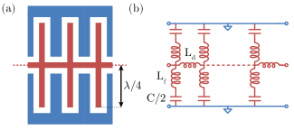
While in conventional traveling-wave amplifiers dispersion engineering prevents only pump harmonic generation, we suppress all unwanted parametric conversion processes by designing our KIT as a weakly dispersive artificial transmission line. Originally developed to have the KIT matched to 50 Ω Chaudhuri et al. (2017), this line consists of a series of coplanar waveguide (CPW) sections, or cells, each with inductance , flanked by two interdigitated capacitor (IDC) fingers that form the capacitance to ground , such that Ω, see Fig. 1a. Each IDC finger then constitutes a low-Q quarter-wave resonator, with capacitance and inductance (see Fig. 1b), set by the finger’s length. In practice, we choose GHz, and , to generate a slight dispersion at low frequencies, where the pump, signal and idler modes lie. The dashed line in Fig. 2a shows the dispersive part of the wavenumber with , as a function of frequency. It is calculated by cascading the ABCD matrices of the KIT cells, see appendix B. As it slightly deviates from zero, no triplet can satisfy Eq. 2.
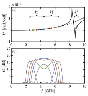
To retrieve phase-matching over a desired bandwidth, we engineer another dispersion feature by increasing the line impedance periodically on short sections. This feature creates a resonance in the line’s phase response (and a stopband in the line’s amplitude response), at a frequency controlled by the loading periodicity Chaudhuri et al. (2017); Pozar (2011). Figure 2a shows in a line periodically loaded at Ω, with GHz. Because the nonlinear wavenumber close to resonance varies sharply, there exists values of (above ) for which we can find triplets that satisfy Eq. 2 (examples of their nonlinear parts are shown in colored dots). A slight variation of the pump frequency significantly affects which pair of signal and idler frequencies is phase matched.
At these matched frequencies, the 3WM gain grows exponentially with (in radians per cell), with the KIT length, and with , the relative inductance modulation amplitude generated by the rf current and scaling with . More precisely, the phase matched, small signal power gain can be written as:
| (3) |
where is the total number of cells, see appendix A.2. Typically, when operating our KIT, ; thus, with pH/cell (see Sec. III), we need to get dB at GHz.
Since maximum gain is achieved with phase-matching, influences the gain profile. To calculate this profile, we insert the dispersion relation into the CME, and solve them numerically, see appendix B. Figure 2b shows signal power gain profiles, calculated for the pump frequencies represented in Fig. 2a. As expected, the gain is maximal at the signal and idler frequencies for which the triplets satisfy Eq. 2. When these frequencies are far apart, there is a region in between where phase matching is not sufficient and the gain drops. By reducing , we can lower the distance between phase-matched signal and idler frequencies, and therefore obtain a wideband, flat gain region. Further reducing , we reach the value where phase-matched signal and idler frequencies are equal, beyond what phase matching is nowhere fulfilled anymore, and the gain drops. Fundamentally, the wideband nature of the gain depends on the convexity of the dispersion relation, and therefore on the fingers’ length and capacitance to ground. As or Q increase, is less convex, and thus closer to a broadband, phase-matched situation, but at the cost of allowing extra parametric processes to arise.
III EXPERIMENTAL REALIZATION
Because the kinetic inductance nonlinearity is weak, in practice a KIT comprises a transmission line tens of centimeters long. To maximize this nonlinearity, and to minimize its length, the line as well as IDC fingers are made 1 m wide, and each unit cell is 5 m long, see Fig. 3a and b. Fabricated from a 20 nm thick NbTiN layer on 380 m high-resistivity intrinsic silicon via optical lithography, it yields mA, and a sheet inductance square. Thus, pH, and in order to retrieve Ω, each finger is made 102 m long. The loading (Fig.3a) consists of cells with shorter fingers (33.5 , Ω), arranged periodically to generate a resonance at 8.5 GHz, thereby positioning the pump frequency in a way compatible with our filtering capabilities.
We lay out the line in a spiral topology, on a cm chip (Fig. 3c), which contains cells, equivalent to 33 cm. To avoid spurious chip and microstrip modes, electrical grounding inside the chip is ensured with spring-loaded pogo pins, descending from the top copper lid of the packaging, and contacting the chip between the line traces, see appendix D. The pogo pins also improve the chip-to-packaging thermal link, which otherwise mostly relies on wire-bonds.

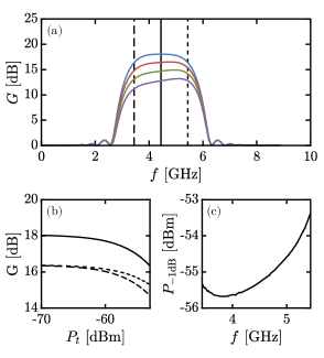
In a first experiment, we measure the gain, bandwidth, and power handling of the KIT when cooled to mK. The KIT is mounted as the sole amplifier in the chain, thereby facilitating comparison of its gain profile to the theoretical profiles, and revealing the gain ripples of the isolated KIT, which otherwise also depend on the return loss of external components. Two mandatory bias tees at the KIT input and output ports combine dc and rf currents. Figure 4a shows KIT gain profiles, acquired at two different pump frequencies. The current amplitudes are mA, and A ( dBm in power, calibrated in situ by comparing dc and rf nonlinear phase shifts, see appendix A.3). For the higher pump frequency, the gain drops in the middle of the amplification bandwidth. For the lower one, the gain profile is flatter, with an average value of dB between 3.5 and 5.5 GHz, where the subscript and superscript denote the amplitude of the gain ripples. Both profiles agree qualitatively with behaviors explained in Sec. II. The gain ripples have a MHz characteristic frequency (see Fig. 4c), equivalent to cm in wavelength (the phase velocity being cell per nanosecond), or about twice the KIT length. We thus attribute their presence to a mismatch in impedance between KIT and microwave feed structures before and after the KIT. This mismatch results in a pump standing wave pattern, which influences the signal amplification, depending on its frequency. Figure 4b shows the gain at 4.5 GHz (obtained at the lower pump power), as a function of , the input power of a probe tone. The gain compresses by 1 dB from its small signal value for dBm, about dB lower than theoretical predictions, see appendix C.2. This discrepancy, suggesting substantial room for improvement, may be due to effects not included in our model, such as standing wave patterns, or defects in the line, which locally lower . Nonetheless, is already about dB higher than JTWPAs Macklin et al. (2015); White et al. (2015); Planat et al. (2020), and about dB less than 4WM KITs with similar gain (see appendix H). This KIT is therefore suitable to read thousands of frequency multiplexed MKIDs, that use drive tone powers typically around dBm Zobrist et al. (2019); Vissers et al. (2016) or even more qubits, whose readout involves powers substantially less than dBm.
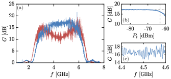
As in any phase-insensitive traveling-wave and resonant parametric amplifier, the practical, usable bandwidth, is half of the presented amplification bandwidth. It is the bandwidth in which signals coming from microwave devices can be phase-insensitively amplified. The other half, barring the idler frequencies, contains a copy of signals in the first half. That is why the gain in Fig. 4a is nearly symmetric about the half pump frequency ( GHz). The asymmetry - gain and ripples marginally bigger above the half pump frequency - originates from a frequency dependent saturation power. In fact, higher frequencies possess a higher saturation power, see appendix C.1. We see this effect here because we chose a signal power close to in order to maximize the signal-to-noise ratio in this measurement, where the KIT remains the sole amplifier.
At higher dc current bias (bounded by the dc critical current of the transmission line, mA in our device), lower rf pump power can be used to obtain equivalent small signal gain, at the cost of a reduced 1 dB compression power. Conversely, reducing and increasing improves power handling capabilities, but the gain is then limited by a superconductivity breaking phenomenon. We suspect the presence of weak links Bockstiegel et al. (2014), and we are currently investigating the line breakdown mechanism.
IV NOISE PERFORMANCE
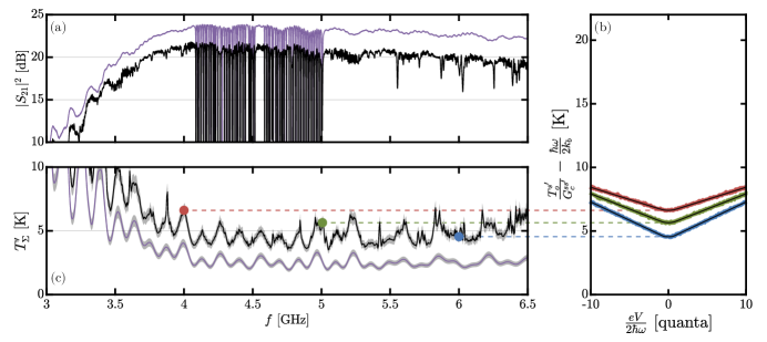
The combined gain, bandwidth, and power handling performance are promising, provided that the KIT also presents competitive noise performance. Measuring this noise is a topic of current interest Eom et al. (2012); Ranzani et al. (2018); Zobrist et al. (2019), and we execute the task using a self-calibrated shot-noise tunnel junction (SNTJ) Spietz et al. (2003, 2006). We measure the output spectral density, whose power depends on the chain’s gain and loss. The SNTJ acts as a dynamic variable noise source, allowing for a continuous sweep in input noise temperature by sweeping its bias voltage, and our measurement scans the entire KIT bandwidth.
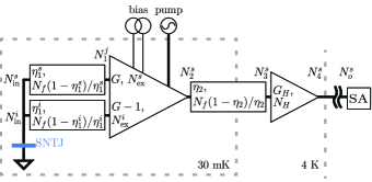
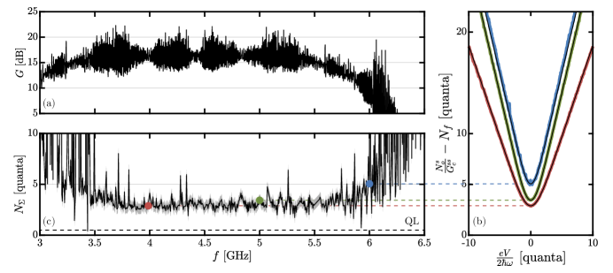
Because the SNTJ is a wideband noise source, it illuminates the KIT at both its signal and idler frequency inputs; these input noises are then parametrically amplified. We thus model the KIT as a three-port network: two inputs at and , and one output at . Figure 5 schematizes the entire amplification chain, where we have labeled the gain or transmission efficiency, and input-referred added noise of each component. The KIT power gain on the signal-to-signal path is , while its power gain on the idler-to-signal path is Caves (1982). The output noise at the signal frequency (in units of photons) measured on the spectrum analyzer (SA) can then be written as
| (4) |
where () is the SNTJ-generated noise at the signal (idler) frequency, () is the signal-to-signal (idler-to-signal) gain of the entire chain from SNTJ to SA, and () is the effective signal-to-signal (idler-to-signal) path KIT-excess noise, see appendix F.1. When varying and we retrieve and , equal to zero for a quantum-limited amplifier.
The system-added noise that a device replacing the SNTJ would see is therefore
| (5) |
where quanta is the vacuum noise (provided that the idler port of this device is cold); for a high gain, phase-insensitive quantum-limited amplifier is the minimum added noise Caves (1982). Failure to account for the additional change in idler noise at the amplifier’s input leads to an underestimate of the system-added noise by about a factor two, thereby making it look significantly better than its true value, given by Eq. 5, see appendix F.2.
In practice, we measure while varying simultaneously and using the SNTJ voltage bias (Fig. 6b). We then fit to obtain , , and (see appendix F.3), and form with Eq. 5. Figure 6c presents the system-added noise , measured over the KIT’s amplification bandwidth. In this experimental configuration, the KIT gain is dB between 3.5 and 5.5 GHz (Fig. 6a), stable over the acquisition time ( hrs). In that bandwidth, quanta. It is an unprecedented broadband, true system-added noise performance (see appendix H).
This performance depends on the intrinsic signal (idler) KIT-excess noise (), but also on the chain’s transmission efficiencies as well as on the HEMT-added noise . More precisely, when , Eq. 5 becomes:
| (6) |
From left to right, the first three terms in the right-hand side represent the contribution to from the KIT alone, from the lossy link between the SNTJ and the KIT, and from the HEMT-added noise; the last term is the minimum half quantum of added noise that a quantum-limited amplifier must add Caves (1982). Measuring the individual loss of the chain’s components, we estimate the value of the transmission efficiencies to be and ; in addition, by measuring the system-added noise of the amplification chain with the KIT turned off, we estimate quanta, see appendix G. With these additional information, we estimate that the overall KIT-excess noise is quanta, suggesting that the KIT alone operates near the quantum limit.
Several strategies can improve the system-added noise. First, increasing the transmission efficiencies would have a major impact, because all the system-dependent noise contributions are enlarged by . For example, would yield quanta. To that end, we are currently developing lossless superconducting circuits (bias tees, directional couplers and low-pass filters) that can be integrated on-chip with the KIT. Second, increasing the KIT gain would reduce the HEMT contribution to (third term in Eq. 6). Here, this contribution is estimated at quanta. The solutions to achieve higher gain directly follow from Eq. 3: higher pump power (i.e. increase ), longer line (increase ), or higher inductance per unit cell (increase ). All represent non-trivial challenges, starting with better understanding of the line breakdown mechanism Bockstiegel et al. (2014). If it comes from imperfections in the line (weak links), a higher resolution fabrication process, like electron beam lithography, may improve the performance of the device. Also, running the amplifier at higher gain will require better damping of the gain ripples, whose amplitude grows with gain. Finally, we are investigating the origin of the remaining excess noise . It may be due to parasitic chip heating or two-level system noise Gao et al. (2008).
V CONCLUSION
It is possible to build a microwave amplifier with broadband and near-quantum-limited performance without sacrificing power handling capability. Engineering the phase-matched bandwidth is key because it suppresses spurious parametric conversion processes. We demonstrate this idea on a KIT, whose combined gain, bandwidth, power handling, and noise performance are fully characterized. In addition, we develop a theoretical framework adapted to noise measurements performed with wideband noise sources. Using a SNTJ we evaluate the true system-added noise of an amplification containing the KIT as the first amplifier. The KIT itself is estimated to be near-quantum-limited, therefore it has the potential to initiate a qualitative shift in the way arrays of superconducting detectors, such as MKIDs, process information, moving them into a quantum-limited readout regime.
Acknowledgments
We thank Kim Hagen for his help in the design and fabrication of the KIT packaging, and Felix Vietmeyer and Terry Brown for their help in the design and fabrication of room temperature electronics. We acknowledge useful discussions with John Teufel, Gangqiang Liu and Vidul Joshi. Certain commercial materials and equipment are identified in this paper to foster understanding. Such identification does not imply recommendation or endorsement by the National Institute of Standards and Technology, nor does it imply that the materials or equipment identified are necessarily the best available for the purpose. This work was supported by the NIST Innovations in Measurement Science Program, as well as NASA, under grant NNH18ZDA001N-APRA.
Appendix A COUPLED-MODE THEORY OF A DC-BIASED KIT
A.1 Coupled-mode equations
The phase matching condition for exponential gain, Eq. 2 is obtained by solving the CME while pumping in a 3WM fashion, i.e. such that , and in the presence of 3WM and 4WM terms see, Eq. 1. The CME relate the current amplitudes , at the frequencies , ; they are obtained by injecting equation 1 into the telegrapher’s equations, and by operating the harmonic balance (HB) with only these three frequencies.
More precisely, the telegrapher’s equations in a lossless transmission line relate current I and voltage V as:
| (7) | ||||
with x a length per unit cell. Injecting Eq. 1 into Eqs. 7, we obtain:
| (8) |
with the phase velocity. To solve Eq. 8 we perform the HB: we assume that the current in the transmission line is a sum of three terms at three different frequencies:
| (9) | ||||
and we then keep only the mixing terms from Eq. 8 that emerge at these frequencies. This approach is valid in our case, because the phase matching bandwidth is limited by dispersion engineering (see appendix B), and thus mostly these three frequencies are able to mix together. Under the slow-varying envelope approximation, for , the left hand side of Eq. 8 yields:
| (10) |
Using , we collect terms at , in the right hand side (rhs) and form the CME:
| (11) | ||||
with . The phase matching condition, Eq. 2, is found for a strong pump, where . Assuming the pump undepleted, , Eqs. 11 rewrite:
| (12) | ||||
which results in . Signal and idler amplitudes are then searched with the form: , . Equations 12 then yield:
| (13) | ||||
with and . The system of equations 13 has known solutions Boyd (2019). In particular, when phase matching is achieved, i.e. , we obtain:
| (14) | ||||
with , and with initial conditions and . The signal power gain
| (15) |
is then exponential with : .
A.2 3WM gain
We can re-write as a function of more meaningful quantities. In fact, the linear inductance exposed in Eq. 1 also writes:
| (16) | ||||
when , and with . Here, is the bare linear inductance. It is the one directly derived from the sheet kinetic inductance and the geometry of the line, while is the inductance per unit length under dc bias. Because , for design purposes . In the strong pump regime , therefore, ; assuming , we therefore get:
| (17) |
where
| (18) |
is the relative inductance variation due to . With mA, and typical values: mA (limited by the dc critical current, mA, value specific to our NbTiN film and to the line’s width) and , we get .
A.3 Pump phase shift
From the phase matching condition, Eq. 2, it is clear that only the 4WM term creates a dispersive phase shift of pump, signal and idler. In other words, in a pure 3WM case, and the phase matching condition becomes , naturally fulfilled in a dispersion-less transmission line. While detrimental for noise properties (see Sec. IV), we can use the continued presence of 4WM to our advantage, because it allows us to calibrate the pump power, down to the KIT input.
In fact, in such a situation and influence the pump tone phase shift, which we can measure unambiguously (i.e. not ) with a VNA. More precisely, although the phase read by a VNA is -wrapped, its shift from an initial value can be continuously monitored when and vary, and thus unambiguously determined. This phase shift in turn translates into a wavenumber variation . If initially at zero dc bias and small rf pump amplitude, then , with the pump wavenumber, dependent on and , and the linear wavenumber. When a single pump tone travels along the line (no input signal), we are by default under the strong pump approximation, and the first equation of Eqs. 12 gives . In addition, the current I in the line then writes as , and thus the pump wavenumber is , which leads to . Because , we can rewrite:
| (19) |
therefore and induce similar phase shift in the line. Knowing (room temperature parameter), we thus get at the KIT input.
Appendix B ABCD TRANSFER MATRICES
The dispersion relations, Fig. 2a are calculated by cascading the ABCD matrices of the KIT cells, a method suitable for any periodic loading pattern. We then compute the KIT scattering parameter as Pozar (2011), where Ω is the input and output ports impedance, and finally get .
In the unloaded case, represented in Fig. 1, the ABCD matrix cell is:
| (20) |
All the cells being identical, the KIT’s ABCD matrix is simply . In Fig. 2a we used to match the length of our fabricated KIT, and pH, fF, and nH, values that match our design (fingers are m long and m wide).
In the loaded case, some cells have shorter fingers, see Fig. 3a. In these cells, the capacitance to ground is , where is the load impedance, and a finger’s inductance is . To compute the KIT scattering parameter, we form the ABCD matrix of the repetition pattern comprised with unloaded and loaded cells:
| (21) | ||||
where is the number of unloaded cells and is the number of loaded cells in the pattern, which we call a supercell. As before, to get the KIT’s ABCD matrix, we simply form , where is the number of supercells in the KIT. Here, (equivalent to m), (equivalent to m), (equivalent to cm), therefore . The plain line in Fig. 2a shows the wavenumber thus found, with Ω, and pH, as the finger length in a loaded cell is m .
To compute the signal power gain, Fig. 2b, we inject the expression of for a periodically loaded KIT (from ) in the CME, Eqs. 11. We solve them numerically for different pump frequencies. For GHz (blue curve), GHz (red), GHz (green) and GHz (purple), phase matched signal and idler are detuned from the half pump frequency by , , and GHz respectively. For GHz (gray curve), phase matching is nowhere achieved. We used , mA, mA, and the initial conditions , , and , close to experimental values.
Appendix C KIT SATURATION
C.1 Strong signal gain profile asymmetry
When the input signal power amounts to a significant fraction of the pump power, parametric amplification depletes the pump. It surprisingly generates asymmetry in the signal gain profile, with respect to the half pump frequency. Figure 7a shows signal gain profiles, calculated when phase matching is achieved at exactly half the pump frequency, i.e. for (corresponding to GHz), at various initial signal powers . They are obtained by solving the CME 11, which incorporate pump depletion effects. As increases, the gain diminishes, and the originally flat profile tilts, with higher frequencies presenting higher gain.
Fundamentally, this asymmetry stems from the fact that when solving the CME in the case where varies along the KIT transmission line, the initial conditions (ICs) vary as a function of frequency. More precisely, the second and third equations in Eqs. 11, govern the evolution of and respectively; in a simplified version, they write as
| (22) | ||||
We dropped the second terms in the rhs of Eqs. 11, representing the 4WM conversion processes, as the asymmetry still holds when , and we assumed perfect phase matching in 3WM, , i.e. a dispersionless line.
In the undepleted pump regime , and we can decouple the equations on and . Deriving with respect to Eqs. 22, we get
| (23) |
with , and , as defined in appendix A.1. Using the ICs and (because ), , as seen in Eqs. 14. Signal and idler wavenumbers appear as a product in this solution, hence for any the signal amplitude is symmetric with respect to the half pump frequency.
In the soft pump regime, where is not constant, Eqs. 22 cannot be decoupled. We can however write them in a canonical form, deriving with respect to :
| (24) |
with . Here, the interplay between and comes from , which contains the product (see Eqs. 11). Although signal and idler wavenumbers also appear only as a product in Eqs. 24, these CME lead to an asymmetric signal amplitude profile, because out of the five ICs required to solve them, one changes with frequency: , , , , and . This last IC depends on , which depends on the signal frequency. In the small signal limit, , and we recover a symmetric gain profile with respect to the half pump frequency.
C.2 Compression power calculation
This asymmetry produces higher power handling capabilities at frequencies above , compared to below . Thus, considering that only half the bandwidth is usable for resonator readout, it is more advantageous to have these lie above . Figure 7b shows the gain as a function of a probe tone power , calculated from the CME 11 at three frequencies: one at , and two at GHz. Because phase matching is set to be optimal at , gain is maximal at this frequency. The small signal gain is identical for GHz, however it visibly compresses at higher tone power for GHz. Figure 7c presents the 1 dB compression power , calculated in the interval gigahertz. As expected, is a few dB higher when . This phenomenon is reminiscent of gain distortion, seen in JPAs Malnou et al. (2018). Effects not included in the CME 11, such as standing wave patterns, or defects in the line, which locally lower , may cause the discrepancy between these theoretical calculations and the measurements (see Sec. III)
Appendix D KIT PACKAGING
There are three main concerns when packaging a KIT: first, the package should be matched to 50 Ω. Any mismatch will result in reflections, creating gain ripples (see Sec. III). Second, the package should ensure good electrical grounding of the transmission line. Otherwise, given the fairly large chip size, spurious chip modes can appear within the frequency range of interest. Third, the package should ensure good thermalization inside the chip. Because the pump power remains high for millikelvin operations, any inhomogeneous rise in temperature may trigger a hot spot near a weak-link, and possibly break superconductivity. We implemented a series of technologies to address these concerns.
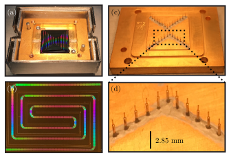
Figure 8a presents the chip, clamped onto the bottom part of the copper packaging. The chip is wire-bonded on both sides to printed circuit boards (PCBs). They convert the on-chip CPW layout to microstrip, and then the central pin of sub-miniature version A (SMA) connectors are soldered onto the microstrip. We suspect imperfect PCBs, with measured impedance close to 52 Ω, play a role in creating gain ripples. When designing the spiral, we carefully adjusted the radius of the turns, in conjunction with the unit cell length, to have these turns match the straight sections’ inductance and capacitance per length.
Electrical grounding inside the chip is ensured with pogo pins inserted in the top lid of the packaging, see Fig. 8c and d. When closing the box, these pins contact the chip between the line traces. If absent, we have measured spurious resonant modes with harmonics at gigahertz frequencies. Pins are m in diameter, and each applies a 20 g force to the chip.
These pins also act as thermal links to the packaging. In addition, we deposited gold strips onto the NbTiN layer, inside the spiral, between the KIT line traces, and near the chip edges, see Fig. 8b. These strips contact the pins. Absent the pogo pins, superconductivity breaks down before high gain can be reached. Finally, we gold-bond the chip ground plane (from the deposited gold) to the copper box (instead of using standard aluminum bonding): gold remains a normal metal at millikelvin temperatures, thereby better thermalizing the chip.
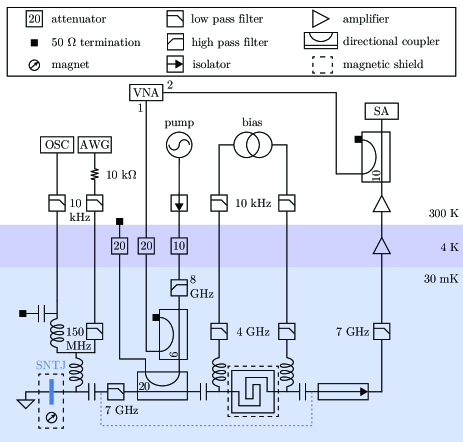
Appendix E NOISE MEASUREMENT EXPERIMENTAL SETUP
Figure 9 presents a schematic of the full experimental setup used to measure the system-added noise of a readout chain using a KIT as a pre-amplifier. In total, noise generated by the SNTJ travels through three amplifiers: the KIT, a HEMT at 4K, and a room temperature amplifier, before finally being recorded with a SA.
The SNTJ is packaged with a permanent magnet suppressing the Josephson effect, and a magnetic shield protects other elements from this magnetic field. In addition, a bias tee routes SNTJ-generated rf noise to the microwave readout chain, while at the same time allowing for dc bias. In fact, the SNTJ is biased with an arbitrary waveform generator (AWG). It outputs a low frequency (50 Hz) triangular voltage wave on a kΩ current limiting resistor, thereby creating a current , varying between A, which sweeps the SNTJ-generated noise value.
An oscilloscope reads the SNTJ voltage in situ while the AWG outputs a known current, allowing the computation of the SNTJ impedance Ω, and with it, the SNTJ voltage bias .
Noise from the SNTJ is combined with rf tones (pump, and probe from a VNA to measure the gain profile) via a 20 dB directional coupler (DC) connected to the KIT input. Additionally, a 7 GHz low-pass filter placed between the SNTJ and the DC prevents the rf pump from leaking back to the SNTJ. Because the KIT requires a fairly high pump power ( dBm), we only attenuate the pump line by 10 dB at 4K. Then, an 8 GHz high-pass filter at 30 mK rejects noise at frequencies within the KIT amplification band, while allowing the pump to pass. A bias tee at the KIT input port combines rf signals (including noise from the SNTJ) with the KIT dc current bias, and a second bias tee at the KIT output separates dc from rf. The rf signal then passes through a GHz isolator, and a 7 GHz low-pass filter (Pasternack PE87FL1015, dB rejection at 9 GHz), preventing the pump tone from saturating the HEMT.
The SA is operated in a zero-span mode, its acquisition triggered by the AWG. This measures the output noise at a single frequency, over a 5 MHz resolution bandwidth (RBW), and directly traces out the curves of Fig. 6b. Varying the SA center frequency, we obtain the system-added noise over the full 3-6.5 GHz bandwidth, Fig. 6c.
Appendix F NOISE THEORY
F.1 System-added noise
When propagating through the experimental setup presented in Fig. 9, noise generated by the SNTJ undergoes loss and amplification. Both processes affect the effective noise at each amplifier input, and therefore also, the noise reaching the SA. While the overall system-added noise encompasses microwave loss, we derive its complete expression as a function of signal () and idler () amplifier-excess noise, gain, and transmission efficiencies to estimate .
Figure 5 represents the lossy amplification chain, with the transmission efficiencies, gain and added noise associated with each interconnection and amplification stages. We have:
| (25) | ||||
| (26) | ||||
| (27) | ||||
| (28) | ||||
| (29) |
Here, with is the KIT-input noise at the signal and idler frequency respectively; then, at the signal frequency, is the KIT-output noise, is the HEMT-input noise, is the HEMT-output noise, and is the noise measured by the SA. Note that the beamsplitter interaction between the KIT and the HEMT assumes the loss to be mostly cold, which is the case in our setup where the lossy components before the HEMT are at the 30 mK stage. Refer to table 1 for the other variable definitions. From Eqs. 25-29 we can derive:
| (30) | ||||
| (31) |
where
| (32) | ||||
| (33) |
and where
| (34) | ||||
| (35) |
The system-added noise is defined as the part of the output noise in Eq. 31 that is not due to the input , and by assuming a cold input at the idler port, i.e. assuming . We thus find
| (36) |
This equation is equivalent to Eq. 5, where we did not simplify the ratio .
F.2 Discarding the idler port input noise
In a simple case where , and , Eq. 30 becomes
| (40) |
Thus, varying the SNTJ bias i.e. and simultaneously, the y-intercept gives , equal to zero for a quantum-limited amplifier. Also, in that simple case, the system-added noise is , as shown by Eq. 36.
On the other hand, if the calibrated noise (coming from the SNTJ or any other wideband noise source, such as a hot/cold load, or a variable temperature stage) only illuminates the signal port of the amplifier, or if the noise at the idler port is wrongly discarded from the analysis, we get and Eq. 30 becomes
| (41) |
Usually, no distinction is made between and , and the effective excess noise is simply . The sum is then what is commonly defined as the system-added noise. Varying the SNTJ bias, i.e. , the y-intercept gives , equal to half a quantum for a quantum-limited amplifier.
In practice, we fit Eqs. 40 or 41 to find the chain’s gain and the y-intercept. Fitting a situation correctly described by Eq. 40 with Eq. 41 leads to an underestimate of the system-added noise. In fact, assuming , Eq. 40 can be rewritten into a form comparable to Eq. 41:
| (42) |
The interpretation of the y-intercept is crucial. Here, the fit yields as the y-intercept, and as the chain’s gain. The true system-added noise is then twice the y-intercept value plus a half quantum, , and the true chain’s gain is half of the fitted slope. Conversely, assuming Eq. 41 leads to the conclusion that the y-intercept value is already the system-added noise, and that the slope is the chain’s gain. The true system-added noise is thus more than twice as high, and the chain’s true gain is half as much (i.e. 3 dB lower, a mistake usually hard to detect).
F.3 Shot-noise fit
The SNTJ generates a known noise power Spietz et al. (2006). The amount of noise , with delivered to the 50 Ω transmission line can be written as Lecocq et al. (2017)
| (43) | ||||
where T is the physical temperature of the SNTJ, and V the SNTJ voltage bias. In practice, the AWG has a slight voltage offset, which we include as a fit parameter: we write instead of V in Eq. 43. In a first step we fit the asymptotes of the output noise response, for which quanta. In that case, Eq. 43 reduces to , and thus Eq. 30 reduces to
| (44) | ||||
We thus get , and . In a second step, we fix , and to their values derived in the first step and fit the central region (where quanta) to Eq. 30 to get , and T.
The spectrum analyzer (SA) records a power spectrum (in Watts), which we convert into a number of photons: , where B is the SA resolution bandwidth. Dividing by , we then refer to the chain’s input. Finally, we can subtract (in quanta), to visually read at on the SNTJ curves of Fig. 6b. In fact,
| (45) |
At ,
| (46) |
where , therefore if , . Considering that , Eq. 45 yields:
| (47) |
F.4 List of variables
| variable name | definition |
|---|---|
| SNTJ-generated noise at the signal frequency | |
| SNTJ-generated noise at the idler frequency | |
| vacuum (or thermal) noise, set by the refrigerator temperature | |
| signal-to-signal path KIT-excess noise | |
| idler-to-signal path KIT-excess noise | |
| signal-to-signal path effective KIT-excess noise, Eq. 34 | |
| idler-to-signal path effective KIT-excess noise, Eq. 35 | |
| HEMT-added noise | |
| noise measured by the SA at the signal frequency, Eq. 30 | |
| noise measured by the SA when the KIT is off, Eq. 38 | |
| system-added noise, Eq. 36 | |
| system-added noise when the KIT is off, Eq. 39 | |
| transmission efficiency between SNTJ and KIT at the signal frequency | |
| transmission efficiency between SNTJ and KIT at the idler frequency | |
| transmission efficiency between KIT and HEMT at the signal frequency | |
| KIT signal power gain | |
| HEMT signal power gain | |
| room-temperature signal power gain | |
| signal-to-signal chain’s gain, Eq. 32 | |
| idler-to-signal chain’s gain, Eq. 33 |
Appendix G LOSS BUDGET IN THE NOISE MEASUREMENT SETUP
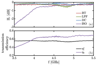
To quote the KIT-excess noise terms and , it is necessary to account for the transmission efficiencies (and therefore the loss) in the measurement setup, , and . Note that is simply the transmission efficiency at the idler frequency , symmetric of the signal frequency with respect to the half-pump frequency . Thus, a broadband measurement of on both sides of provides both and . We estimate these efficiencies in this appendix and give an overall loss budget per component between the SNTJ and the HEMT. Knowing where the loss comes from also provides guidance on how to improve the amplifier because many lossy components could be optimized, particularly by integrating them on-chip with the KIT.
G.1 System-added noise temperature with un-pumped KIT
First, we measured the system-added noise temperature of the amplification chain (with the reduced Planck’s constant and the Boltzmann’s constant) when the KIT is off, i.e. with the HEMT as the first amplifier. In that case, is given by Eq. 39. We measured in two situations: one for the measurement setup presented in Fig. 9, and one where the KIT surrounded by its two bias tees, the directional coupler and the low pass filter next to it have been bypassed, i.e. replaced by a microwave cable. In the limit where , the ratio in between these two situations gives direct access to the bypassed components’ insertion loss (IL) (the exact transmission efficiency ratio from which we calculate is equivalent to finding in Eq. 39). Figure 10c shows as a function of frequency, obtained from fitting curves like those presented in Fig. 10b, obtained with and without the bypass. There are ripples with 130 MHz characteristic frequency, likely due to reflections in coaxial cables between the SNTJ and the HEMT. Without the bypass K between 3.5 and 5.5 GHz, while with the bypass K. Thus, the ratio gives dB.
G.2 Component loss
Second, we replaced the SNTJ (including the bias tee) with a transmission line, to measure the transmission of a probe tone through the setup (with a VNA). This transmission line is capacitively coupled to an array of resonators, whose resonant frequencies span between and GHz, and is part of a future experiment. These resonances are not relevant for the current characterization. We measured the transmission with and without the bypass, shown in Fig. 10a. Once again, the transmission ratio between these two situations gives direct access to the bypassed components’ IL. We find dB, in agreement with the system-added noise measurements of Fig. 10c.
| authors | mixing |
|
|
|
|
|
|
||||||||||||
|---|---|---|---|---|---|---|---|---|---|---|---|---|---|---|---|---|---|---|---|
| this work | 3WM | 2 | - GHz | ||||||||||||||||
| Eom et.al. Eom et al. (2012) | 4WM | Hz | 111idler noise input not accounted for | ||||||||||||||||
| Bockstiegel et.al. Bockstiegel et al. (2014) | 4WM | - | - | - | |||||||||||||||
| Vissers et.al. Vissers et al. (2016) | 3WM | 222at dB gain | - | - | |||||||||||||||
| Chaudhuri et.al. Chaudhuri et al. (2017) | 4WM | - | - | - | |||||||||||||||
| Ranzani et.al. Ranzani et al. (2018) | 3WM | - | - GHz | - | |||||||||||||||
| Zobrist et.al. Zobrist et al. (2019) | 3WM | 333data quoted but not shown in the paper | 1 MHz |
We also measured the individual transmissions of the chain’s components at 4K: bias tee (BT), filter (LPF), directional coupler (DC) and isolator (ISO). Figure 11a shows the IL of these four components. Between and GHz, dB, dB, dB, and dB. Its IL increases below GHz as we leave its operating band, which degrades the system-added noise performance in the same manner as reducing the KIT gain would, see Eq. 34. The SNTJ packaging loss, including the bias tee, has been previously reported to be dB (transmission efficiency of ) Chang et al. (2016).
G.3 HEMT-added noise, transmission efficiencies, KIT-excess noise
We can estimate the HEMT-added noise temperature from eq. 39, because we measured (see Fig. 10c), and because we can have an estimation of the total IL from the SNTJ to the HEMT. In fact, without the bypass
| (48) |
(in dB), which gives dB. Then, , and we get K (i.e. quanta) between 3.5 and 5.5 GHz, in agreement with the HEMT data sheet, which gives K in that frequency range.
Subtracting , and from , the KIT’s packaging (see Fig. 8a) is responsible for about dB of IL. This loss may be decreased in future optimization, for example by coating the PCBs and the SMA pins with superconducting material.
Finally, we can separately estimate and by adding (in dB) the IL of the chain’s components, and then use Eqs. 34 and 35 to estimate the KIT-excess noise and . Between the SNTJ and the KIT,
| (49) |
which gives dB, and between the KIT and the HEMT
| (50) |
which gives dB. Figure 11b shows and thus obtained. Therefore, between 3.5 and 5.5 GHz, (both equal since the frequency band is nearly symmetric with respect to GHz), and .
Appendix H KIT PERFORMANCE COMPARISON
Table 2 compares the performance of our KIT with previous results on KITs. The pump power (third column) is the power at the KIT’s input. The gain (fourth column) is the average gain observed over the KIT amplification bandwidth (fifth column). The amplitude of gain ripples over that bandwidth is indicated next to the gain value. The saturation power (sixth column) corresponds to the input dB compression point. The noise bandwidth (seventh column) is the bandwidth over which a noise measurement was performed. Finally, column eight reports the measured system noise temperature in that bandwidth. In our case, quanta, which translates into K. Note that Eom et.al Eom et al. (2012), Ranzani et.al. Ranzani et al. (2018) and Zobrist et.al. Zobrist et al. (2019) used a wideband noise source (a hot/cold load) but did not account for the effect of the idler port’s input noise. Therefore, their true system-added noise is about twice of what they reported (see appendix F.2). We do not compare the amplifier-added noise or amplifier-excess noise, because it is subject to approximations in the amount of loss present in the noise measurement setup. In addition, the inferred added noise usually does not include the loss of mandatory microwave components used when operating the amplifier, and as such it is an under-estimation of the true, useful amplifier-added noise.
References
- Castellanos-Beltran et al. (2008) M. A. Castellanos-Beltran, K. D. Irwin, G. C. Hilton, L. R. Vale, and K. W. Lehnert, “Amplification and squeezing of quantum noise with a tunable Josephson metamaterial,” Nature Physics 4, 929–931 (2008).
- Bergeal et al. (2010) N. Bergeal, F. Schackert, M. Metcalfe, R. Vijay, V. E. Manucharyan, L. Frunzio, D. E. Prober, R. J. Schoelkopf, S. M. Girvin, and M. H. Devoret, “Phase-preserving amplification near the quantum limit with a josephson ring modulator,” Nature 465, 64–68 (2010).
- Roch et al. (2012) N. Roch, E. Flurin, F. Nguyen, P. Morfin, P. Campagne-Ibarcq, M. H. Devoret, and B. Huard, “Widely tunable, nondegenerate three-wave mixing microwave device operating near the quantum limit,” Phys. Rev. Lett. 108, 147701 (2012).
- Mutus et al. (2013) J. Y. Mutus, T. C. White, E. Jeffrey, D. Sank, R. Barends, J. Bochmann, Yu Chen, Z. Chen, B. Chiaro, A. Dunsworth, J. Kelly, A. Megrant, C. Neill, P. J. J. O’Malley, P. Roushan, A. Vainsencher, J. Wenner, I. Siddiqi, R. Vijay, A. N. Cleland, and John M. Martinis, “Design and characterization of a lumped element single-ended superconducting microwave parametric amplifier with on-chip flux bias line,” Applied Physics Letters 103, 122602 (2013).
- Zhong et al. (2013) L. Zhong, E. P. Menzel, R. Di Candia, P. Eder, M. Ihmig, A. Baust, M. Haeberlein, E. Hoffmann, K. Inomata, T. Yamamoto, Y. Nakamura, E. Solano, F. Deppe, A. Marx, and R. Gross, “Squeezing with a flux-driven josephson parametric amplifier,” New J. Phys. 15, 125013 (2013).
- Lecocq et al. (2017) F. Lecocq, L. Ranzani, G. A. Peterson, K. Cicak, R. W. Simmonds, J. D. Teufel, and J. Aumentado, “Nonreciprocal microwave signal processing with a field-programmable josephson amplifier,” Phys. Rev. Applied 7, 024028 (2017).
- Malnou et al. (2018) M. Malnou, D. A. Palken, Leila R. Vale, Gene C. Hilton, and K. W. Lehnert, “Optimal operation of a josephson parametric amplifier for vacuum squeezing,” Phys. Rev. Applied 9, 044023 (2018).
- Mutus et al. (2014) J. Y. Mutus, T. C. White, R. Barends, Yu Chen, Z. Chen, B. Chiaro, A. Dunsworth, E. Jeffrey, J. Kelly, A. Megrant, C. Neill, P. J. J. O’Malley, P. Roushan, D. Sank, A. Vainsencher, J. Wenner, K. M. Sundqvist, A. N. Cleland, and John M. Martinis, “Strong environmental coupling in a josephson parametric amplifier,” Applied Physics Letters 104, 263513 (2014).
- Roy et al. (2015) T. Roy, S. Kundu, M. Chand, A. M. Vadiraj, A. Ranadive, N. Nehra, M. P. Patankar, J. Aumentado, A. A. Clerk, and R. Vijay, “Broadband parametric amplification with impedance engineering: Beyond the gain-bandwidth product,” Applied Physics Letters 107, 262601 (2015).
- Frattini et al. (2017) N. E. Frattini, U. Vool, S. Shankar, A. Narla, K. M. Sliwa, and M. H. Devoret, “3-wave mixing josephson dipole element,” Applied Physics Letters 110, 222603 (2017).
- Frattini et al. (2018) N. E. Frattini, V. V. Sivak, A. Lingenfelter, S. Shankar, and M. H. Devoret, “Optimizing the nonlinearity and dissipation of a snail parametric amplifier for dynamic range,” Phys. Rev. Applied 10, 054020 (2018).
- Sivak et al. (2019) V. V. Sivak, N. E. Frattini, V. R. Joshi, A. Lingenfelter, S. Shankar, and M. H. Devoret, “Kerr-free three-wave mixing in superconducting quantum circuits,” Phys. Rev. Applied 11, 054060 (2019).
- Macklin et al. (2015) C. Macklin, K. O’Brien, D. Hover, M. E. Schwartz, V. Bolkhovsky, X. Zhang, W. D. Oliver, and I. Siddiqi, “A near–quantum-limited josephson traveling-wave parametric amplifier,” Science 350, 307–310 (2015).
- White et al. (2015) T. C. White, J. Y. Mutus, I.-C. Hoi, R. Barends, B. Campbell, Yu Chen, Z. Chen, B. Chiaro, A. Dunsworth, E. Jeffrey, J. Kelly, A. Megrant, C. Neill, P. J. J. O’Malley, P. Roushan, D. Sank, A. Vainsencher, J. Wenner, S. Chaudhuri, J. Gao, and J. M. Martinis, “Traveling wave parametric amplifier with josephson junctions using minimal resonator phase matching,” Applied Physics Letters 106, 242601 (2015).
- Planat et al. (2020) L. Planat, A. Ranadive, R. Dassonneville, J. Puertas Martínez, S. Léger, C. Naud, O. Buisson, W. Hasch-Guichard, D.M. Basko, and N. Roch, “Photonic-crystal josephson traveling-wave parametric amplifier,” Phys. Rev. X 10, 021021 (2020).
- Sivak et al. (2020) V. V. Sivak, S. Shankar, G. Liu, J. Aumentado, and M. H. Devoret, “Josephson array-mode parametric amplifier,” Phys. Rev. Applied 13, 024014 (2020).
- Zorin (2016) A. B. Zorin, “Josephson traveling-wave parametric amplifier with three-wave mixing,” Phys. Rev. Applied 6, 034006 (2016).
- Zorin (2019) A.B. Zorin, “Flux-driven josephson traveling-wave parametric amplifier,” Phys. Rev. Applied 12, 044051 (2019).
- Eom et al. (2012) B. H. Eom, P. K. Day, H. G. LeDuc, and J. Zmuidzinas, “A wideband, low-noise superconducting amplifier with high dynamic range,” Nature Physics 8, 623–627 (2012).
- Arute et al. (2019) F. Arute et al., “Quantum supremacy using a programmable superconducting processor,” Nature 574, 505–510 (2019).
- Shor (1994) P. W. Shor, “Algorithms for quantum computation: discrete logarithms and factoring,” in Proceedings 35th Annual Symposium on Foundations of Computer Science (IEEE, 1994) pp. 124–134.
- Grover (1997) L. K. Grover, “Quantum mechanics helps in searching for a needle in a haystack,” Phys. Rev. Lett. 79, 325–328 (1997).
- Szypryt et al. (2017) P. Szypryt, S. R. Meeker, G. Coiffard, N. Fruitwala, B. Bumble, G. Ulbricht, A. B. Walter, M. Daal, C. Bockstiegel, G. Collura, N. Zobrist, I. Lipartito, and B. A. Mazin, “Large-format platinum silicide microwave kinetic inductance detectors for optical to near-ir astronomy,” Opt. Express 25, 25894–25909 (2017).
- Hochberg et al. (2016a) Y. Hochberg, Y. Zhao, and K. M. Zurek, “Superconducting detectors for superlight dark matter,” Phys. Rev. Lett. 116, 011301 (2016a).
- Hochberg et al. (2016b) Y. Hochberg, M. Pyle, Y. Zhao, and K. M. Zurek, “Detecting superlight dark matter with fermi-degenerate materials,” Journal of High Energy Physics 2016, 57 (2016b).
- Chaudhuri et al. (2017) S. Chaudhuri, D. Li, K. D. Irwin, C. Bockstiegel, J. Hubmayr, J. N. Ullom, M. R. Vissers, and J. Gao, “Broadband parametric amplifiers based on nonlinear kinetic inductance artificial transmission lines,” Applied Physics Letters 110, 152601 (2017).
- Zobrist et al. (2019) N. Zobrist, B. H. Eom, P. Day, B. A. Mazin, S. R. Meeker, B. Bumble, H. G. LeDuc, G. Coiffard, P. Szypryt, N. Fruitwala, I. Lipartito, and C. Bockstiegel, “Wide-band parametric amplifier readout and resolution of optical microwave kinetic inductance detectors,” Applied Physics Letters 115, 042601 (2019).
- Spietz et al. (2003) L. Spietz, K. W. Lehnert, I. Siddiqi, and R. J. Schoelkopf, “Primary electronic thermometry using the shot noise of a tunnel junction,” Science 300, 1929–1932 (2003).
- Spietz et al. (2006) L. Spietz, R. J. Schoelkopf, and P. Pari, “Shot noise thermometry down to 10mk,” Applied Physics Letters 89, 183123 (2006).
- Vissers et al. (2016) M. R. Vissers, R. P. Erickson, H.-S. Ku, L. Vale, X. Wu, G. C. Hilton, and D. P. Pappas, “Low-noise kinetic inductance traveling-wave amplifier using three-wave mixing,” Applied Physics Letters 108, 012601 (2016).
- Erickson and Pappas (2017) R. P. Erickson and D. P. Pappas, “Theory of multiwave mixing within the superconducting kinetic-inductance traveling-wave amplifier,” Phys. Rev. B 95, 104506 (2017).
- Pozar (2011) D.M. Pozar, Microwave Engineering, 4th Edition (Wiley, 2011).
- Bockstiegel et al. (2014) J. Bockstiegel, C.and Gao, M.R. Vissers, M. Sandberg, S. Chaudhuri, A. Sanders, L.R. Vale, K.D. Irwin, and D.P. Pappas, “Development of a broadband nbtin traveling wave parametric amplifier for mkid readout,” Journal of Low Temperature Physics 176, 476–482 (2014).
- Ranzani et al. (2018) L. Ranzani, M. Bal, Kin Chung Fong, G. Ribeill, X. Wu, J. Long, H.-S. Ku, R. P. Erickson, D. Pappas, and T. A. Ohki, “Kinetic inductance traveling-wave amplifiers for multiplexed qubit readout,” Applied Physics Letters 113, 242602 (2018).
- Caves (1982) Carlton M. Caves, “Quantum limits on noise in linear amplifiers,” Phys. Rev. D 26, 1817–1839 (1982).
- Gao et al. (2008) Jiansong Gao, Miguel Daal, Anastasios Vayonakis, Shwetank Kumar, Jonas Zmuidzinas, Bernard Sadoulet, Benjamin A. Mazin, Peter K. Day, and Henry G. Leduc, “Experimental evidence for a surface distribution of two-level systems in superconducting lithographed microwave resonators,” Applied Physics Letters 92, 152505 (2008).
- Boyd (2019) Robert W Boyd, Nonlinear optics (Academic press, 2019).
- Chang et al. (2016) S.-W. Chang, J. Aumentado, W.-T. Wong, and J.C. Bardin, “Noise measurement of cryogenic low noise amplifiers using a tunnel-junction shot-noise source,” in 2016 IEEE MTT-S International Microwave Symposium (IMS) (IEEE, 2016) pp. 1–4.