Observation of photonic spin-momentum locking due to coupling of achiral metamaterials and quantum dots
Abstract
Here, we report observations of photonic spin-momentum locking in the form of directional and chiral emission from achiral quantum dots (QDs) evanescently coupled to achiral hyperbolic metamaterials (HMM). Efficient coupling between QDs and the metamaterial leads to emergence of these photonic topological modes which can be detected in the far field. We provide theoretical explanation for the emergence of spin-momentum locking through rigorous modeling based on photon Green’s function where pseudo spin of light arises from coupling of QDs to evanescent modes of HMM.
Topological photonicsOzawa et al. (2019) is an emerging area where various novel phenomenon like photonic spin Hall effectBliokh et al. (2015a, 2014, b); Van Mechelen and Jacob (2016), photonic topological insulatorsKhanikaev et al. (2013); Rider et al. (2019); Lu et al. (2014a), unidirectional propagation of lightPetersen et al. (2014); Le Feber et al. (2015); Söllner et al. (2015); Rodríguez-Fortuño et al. (2013); O’connor et al. (2014) etc. have been reported using various degrees of freedom of light coupled with advanced design of metamaterial and metasurfacesHigh et al. (2015); Tan et al. (2014). A key feature of topological effects, spin-momentum locking has been reported for photonic systems where extrinsic helicity of light or explicitly chiral emitters are coupled to surface plasmon polaritons(SPP) or waveguide modesRodríguez-Fortuño et al. (2013); Mitsch et al. (2014) in near fieldKapitanova et al. (2014).Various chiral structures have been used to demonstrate chirality in emission including nanofibers with trapped nanoparticles or atoms on it Le Kien et al. (2006); Petersen et al. (2014); Mitsch et al. (2014) and engineered photonic crystal waveguides having chiral modes Söllner et al. (2015); Le Feber et al. (2015); Young et al. (2015); Hughes and Agarwal (2017). Another system which has been widely used to demonstrate photonic topological effects are metamaterials which have several fascinating properties Smith et al. (2004); Fang et al. (2009); Sreekanth et al. (2013); Zhang et al. (2009); Soskin et al. (2016); Zhang et al. (2009); Gao et al. (2015), etc.
A special class of metamaterials which possesses a hyperbolic iso-frequency surface known as hyperbolic metamaterials (HMM) have a number of novel properties like anisotropy and large photonic density of states which can be used for a number of applications Poddubny et al. (2013); Lu et al. (2014b); Biehs et al. (2018, 2016); Starko-Bowes et al. (2015); Berry and Dennis (2003); Krishnamoorthy et al. (2012). The high wavevectors (high-) of an emitter are evanescent in conventional dielectric media but HMM supports propagation of high- wavevectors West et al. (2015); Cortes et al. (2012); Jahani et al. (2018). However, it has not yet been possible to utilize the properties of these modes by transporting them to the far-field. In general, it has been demonstrated that when chiral emitters couple with evanescent high– modes of HMMs unidirectional and chiral emission emerges in the near-fieldGuddala et al. (2019); Kapitanova et al. (2014). HMM provides the extrinsic momentum to photon by making it directional which couples to intrinsic spin of photon (polarisation state of light) analogous to a spin-orbit interaction. However, transport of these photonic topological modes, especially with intrinsically achiral structures, to the far field has not yet been reported.
Here, we report experimental observation and theoretical modeling of photonic topological effects in the form of directional and chiral far field emission from intrinsically achiral semiconductor quantum dots (QDs) coupled to a two dimensional (2D) achiral HMM. We observe clear signatures of directional and chiral emmission from the hybrid system in wavevector resolved emission map in experiments. We report a new regime of spin-momentum locking phenomenon where extrinsic pseudo helicity of light is provided by coupling quantum emitters to evanescent high- modes of HMM. The observed directional and chiral emission, in experiments, coincides with the appearance of strong splitting of the photoluminescence (PL) spectra from the QDs on HMMIndukuri et al. (2017); SM . The observed experimental results are explained reasonably well using rigorous numerical scheme to evaluate electric field distribution using method of photon Green’s function for geometry similar to that used in experiment. Significantly, we also demonstrate the ability to detect the photonic topological modes generated due to the high- evanescent HMM modes to the far-field. Overall, our study provides a methodology to obtain far field photonic spin-momentum locking without having to use chiral emitters or chiral metamaterials.
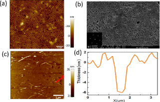
The experimental results are based on fabricated 2D HMM templates consisting of hexagonal arrays of silver nanowires (length ) embedded in alumina matrix prepared using methods described earlier Kanungo and Schilling (2010). A compact monolayer of cadmium selenide (CdSe) QDs, synthesised by well known methodsPeng and Peng (2001); Indukuri et al. (2017); Praveena et al. (2015), was placed on top of the metamaterial using the well known Langmuir-Blodgett (LB) technique as discussed earlier Dabbousi et al. (1994); Haridas et al. (2011) as well as in supplementary materials SM . The metamaterials prepared undergo a wavelength dependent topological transition to a phase having hyperbolic optical dispersion - hence called HMM - depending on silver nanowire filling fraction ( = 0.15 in our study) SM . The peak emission wavelength of the QDs was chosen such that it lies well inside HMM dispersion spectral regime SM . Atomic force microscopy (AFM) and scanning electron microscopy (SEM) image of top surface of HMM is shown in Fig. 1(a) and (b), respectively, reveals the ordered structure of the array as well as the lattice spacing. AFM image of the same template after transfer of a compact QD monolayer on top of a polymer spacer is shown in Fig 1(c) with the thickness of the film () being revealed in a typical height profile in Fig 1(d) roughly correponding to the diameter of the QDs used SM . For back focal plane Fourier imaging the QD monolayers on HMM templates were excited by focusing a 633 nm continuous wave (CW) laser using 100X objective with numerical aperture (NA) being 0.95. Emission was collected by the same objectiveVasista et al. (2018). For PL spectro-microcopy measurements excitation was performed with 514nm laser as described earlier Indukuri et al. (2017) and in SM .
Fig. 2(a) shows schematic of experimental system which demostrates the directional and chiral emission from QD monolayer coupled to HMM. In Fig. 2(b-c), we have shown the Fourier images for QDs on HMM and QD on glass, respectively for spacer layer thickness, = 10nm.
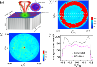
A clear signature of directional emission was observed for QDs placed in the near-field of HMM and emission is azimuthally symmetric and wavevector preferential. Azimuthally symmetric rings of maximum intensity are observed for QDs placed in near-field of HMM at a separation of 10 nm, which is shown in Fig. 2(b). We also performed a reference measurement for same QD monolayer on glass as shown in Fig. 2(c). Figure 2(c) shows a completely isotropic and homogeneous emission from the same QD monolayer on glass. To quantify this data further, we extracted the line profile of emission intensity for a band of at along as indicated in Fig. 2(b)and(c) by a pair of lines. Emission intensity is integrated over a band of to avoid the spatial resolution limited fluctuations in emission intensity. These integrated intensity profiles when plotted as a function in Fig. 2(d) reveal two symmetric peaks of maximum emission intensity for =10nm, whereas for the reference sample (QD on glass) it does not show any wavevector preferential emission. In summary, Fig. 2 manifests that the emergence of directional emission from QDs on HMM is due to the coupling of excitons in QDs to large- modes of HMM.
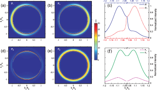
After confirmation of the connection of directional emission with large- modes, we explore the study of the chiral nature of these modes. In general, these large- modes are evanescent in nature. To study this,we excited our system with LCP and RCP polarised CW laser and emission was collected in the Fourier image. Fig. 3 shows LCP and RCP excitation dependent Fourier images for QDs on HMM and QDs on glass systems. It should be noted that we have eliminated the central region( NA= 0 to 0.24) of the Fourier image which has emitted signal of the uncoupled QDs with large- modes of HMM. The resultant Fourier image of LCP and RCP excitation shows a circular ring of maximum intensity followed by a minima located at mutually opposite azimuthal angles () as visible in Fig. 3(a) and (b), which shows the helicity dependent emission. The radius of the ring gives us the directions of emission which are characterized by and .
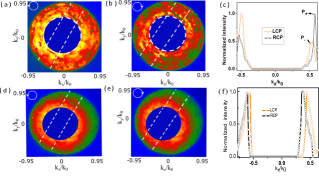
To extract the emission intensity line profiles from the Fourier images, a pair of white dotted lines are drawn in a fixed direction. Extracted emission intensity profile is normalised with maximum intensity of extracted line profile and plotted in Fig. 3(c). Normalised emission intensity profile shows antisymmetric intensity peak for LCP and RCP excitations. For RCP excitation, maximum intensity peak occurs at and the case is reverse for LCP excitation. After confirming the chiral nature of emission from HMM based system, we calculated chirality () using following expression:
| (1) |
where and are local maximum intensity for for LCP and RCP incident polarizations and we have . The value stands for the excitation by using a linear polarization, while implies a truly unidirectional excitation of the field. The chirality parameter was obtained from above mentioned analysis of Fourier image as indicated in Fig. 3(c). We also performed LCP and RCP excitation dependent Fourier imaging for QDs on glass as reference measurement as shown in Fig. 3(d) and 3(e), respectively. Emission intensity line profiles for QDs on glass are plotted in Fig. 3(f) which clearly shows no chiral pattern. Thus, our experimental observations suggest the ability of the QDs to couple HMM high modes leading to observation of spin-momentum locking detectable in far-field. Interestingly , this phenomenon disappears for larger value of spacer thickness,, ( SM , Figure S4), suggesting an intricate connection between the emergence of spin-momentum locking and the observation of splitting of PL spectra for QDs on HMM templates as shown in detail by us earlier Indukuri et al. (2017) and in SM (Figure S3).
Theoretical Modeling
We next develop a model for the observations. We use rigorous solutions of Maxwell equations, i.e., the development is similar to a recent one Liu et al. (2019) but is generalized to the present experimental geometry. Unlike the layered medium in the previous work, the HMM in the present work is different and is characterized by complex effective dielectric tensor. The detailed modeling is given in the Supplementary Material SM . We can numerically investigate the emission characteristics radiating by a two-dimensional dipole on the nanowire HMMs, where the unit dipole moment of the dipole is with . We select the related parameters corresponding to the experiment as: , , , and . In order to make the coupling mechanism clear, we first consider the case of . In this case, the s-polarized waves have no contribution to the electric field intensity from the Eq. (S8)SM . Then the electric field intensity of the p-polarized waves in the Fourier transformed space can be described as Novotny and Hecht (2012)
| (2) |
where and . As discussed in SM , the reflection is symmetric along the . Therefore, the Eq. (2) can be seemed as . For evanescent waves with , the term is a complex number and then . If we let and be real numbers without a phase difference used for the unpolarized case, the electric field intensity can be written as , which is a linear superposition of the contributions from the horizonal and vertical oriented components of the dipole. No interference phenomenon occurs in this case. However, the case is different when and have a phase difference. For instance, for the right-circularly polarized dipoles, we have and . Consequently, the electric field intensity can be reduced to . The horizonal and vertical oriented spectral amplitudes for add up constructively, whereas for destructive interference occurs. Therefore, we emphasize that chiral emission occurs when a circularly polarized dipole excites the multilayered nanostructure. More generally, elliptic polarization with a phase difference of between the and components is required. These very general findings on the expected chiral behaviour are in agreement with the experimental results in Fig. (3). We also disccused the case without absorption in silver, which is given in the SM( figure S7))SM .
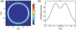
In the following, we give a quantitative analysis about the electric field intensity () for different dipolar polarization states. The unit vector of the horizontally (vertically) polarized dipole is (). For the circularly polarized dipoles, the unit polarization vectors are . The dielectric constant tensor for the HMMs can be described by the effective medium theory, as given in SM , by and for the wavelength .In Fig. 4(a), we present the electric field intensity map induced by the unpolarized dipole with and , which can match well with that in Fig. 2(b) and 2(d). Figure 4(b) shows the normalized emission intensity profile along the direction with . It has two symmetric peaks with approximately equal intensity at , which denotes that there is no chiral behaviour but only directional characteristics.
The intensity maps containing information for both TE and TM modes for different dipolar polarizations are shown in Fig. 5(a-b) and 5(d-e), which give a circular ring of maximum intensity followed by a minima and show directional emission. Moreover, chiral emission for the cases of circularly polarized dipoles with can be found in Fig. 5(a) and 5(b). The electric field profile is asymmetric along the axis in Fig. 5(a-c). According to the Eq. (2), the incident field induced by a left-circularly polarized dipole () couples more efficiently with a forward-propagating mode for , and backward propagation is suppressed for . However, the case for a right-circularly polarized dipole () is converse. For the right-circularly polarized dipole, the position of peak appears at and the peak for appears as a relatively broad shoulder. Even though, emission intensity line profiles still show chiral behaviour for circularly polarized dipoles with at . This theoretical value of is higher than the experimental value. This is because the theoretical result is calculated from the peak value, whereas the experiment data is averaged over a range of vectors. This clearly will bring down the observed value of . Instead, for linearly polarized dipoles, the excited field is bidirectional propagation, as shown in Fig. 4(f). The forward-propagating and backward-propagating modes are symmetrical modal distribution. Electric field intensity of the high- propagating mode induced by a z-polarized dipole is larger than that of an x-polarized dipole. We can find that even though there is no preference in the direction, the directional emission can be realized by using the circularly polarized dipoles.In the experimental data, the measured wave vectors are in free space where as in theoretical modeling and are in glass objective which has refractive index 1.45. A closer look at Fig. 3(a) shows for example that the emission max-min corresponds to about 0.7 which translates to in glass as 1.015 which matches well with the maximum in the Fig. 5(c) obtained in the electromagnetic calculations.
The polarization degree of freedom provides a new approach for studying a variety of novel optical effects. Finally, we show how the dielectric constant tensor and can be used to obtain the chiral character in a simple manner.
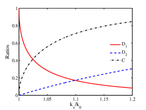
For large- wave vectors (), the intensity ratio between the left-circularly () and right-circularly () polarized components is defined as
| (3) |
where . The chiral parameter can be given by . We can also define the intensity ratio induced by the horizontally and vertically polarized dipoles as
| (4) |
In Fig. 6, we present the intensity ratios ( and ) and chiral parameter () as a function of the wave vector component for and . When increasing the value of , the intensity ratio goes down, while the chiral parameter and intensity ratio grow up. Therefore, we can obtain larger chiral value by properly changing the filling ratio and the emission wavelength. Thus we can estimate the chirality depending on the direction in which emission is dominant. This value of is determined by the properties of the hyperbolic medium and Eq.3 implies the spin momentum locking which we observe in our experiments. In conclusion, we have demonstrated photonic spin-momentum locking in the form of directional and chiral emission from excitons in compact monolayers of QDs efficiently coupled to evanescent metamaterial modes in a 2D HMM. Based on the method of photon Green’s function, the chiral emission from a circularly polarized dipole coupled with HMMs are presented theoretically and the origin of photonic spin-momentum locking in experiments, quantitatively, explained. The origin of chirality is attributed to the near-field interference between the longitudinal and transverse polarized components of the dipolar QDs in evanescent high- modes of the HMM. Equivalently, the directional emission can be observed by exploring a elliptically polarized dipole to break the inversion symmetry, similar to the spin Hall effect. Our study thus provides a method to obtain chiral and directional photonic effects in the far field without having to use chiral emitters or chiral metamaterials.
Acknowledgements.
The authors acknowledge Indo-U.S. Science and Technol-ogy Forum (IUSSTF) for funding through a virtual centre onquantum plasmonics.The authors also acknowledge Scheme for Promotion of academic and Research Collabration(SPARC) for funding.WXL is supported by the National Natural Science Foundation of China (NSFC) (Nos. 11534008, 91536115), and the Natural Science Foundation of Shaanxi Province (No. 2016JM1005). GSA thanks the support from the Welch Foundation (No. A-1943-20180324). GSA also thanks the Infosys Foundation Chair of Department of Physics, IISc Bangalore which made this collaboration successful.GVPK acknowledges the support of Swarnajayanthi fellowship grant - DST/SJF/PSA-02/2017-18 and Center for Energy Science. Grant Number: SR/NM/TP‐13/2016.References
- Ozawa et al. (2019) T. Ozawa, H. M. Price, A. Amo, N. Goldman, M. Hafezi, L. Lu, M. C. Rechtsman, D. Schuster, J. Simon, O. Zilberberg, et al., Reviews of Modern Physics 91, 015006 (2019).
- Bliokh et al. (2015a) K. Y. Bliokh, D. Smirnova, and F. Nori, Science 348, 1448 (2015a).
- Bliokh et al. (2014) K. Y. Bliokh, A. Y. Bekshaev, and F. Nori, Nature communications 5, 1 (2014).
- Bliokh et al. (2015b) K. Y. Bliokh, F. J. Rodríguez-Fortuño, F. Nori, and A. V. Zayats, Nature Photonics 9, 796 (2015b).
- Van Mechelen and Jacob (2016) T. Van Mechelen and Z. Jacob, Optica 3, 118 (2016).
- Khanikaev et al. (2013) A. B. Khanikaev, S. H. Mousavi, W.-K. Tse, M. Kargarian, A. H. MacDonald, and G. Shvets, Nature Materials 12, 233 (2013).
- Rider et al. (2019) M. S. Rider, S. J. Palmer, S. R. Pocock, X. Xiao, P. Arroyo Huidobro, and V. Giannini, Journal of Applied Physics 125, 120901 (2019).
- Lu et al. (2014a) L. Lu, J. D. Joannopoulos, and M. Soljačić, Nature photonics 8, 821 (2014a).
- Petersen et al. (2014) J. Petersen, J. Volz, and A. Rauschenbeutel, Science 346, 67 (2014).
- Le Feber et al. (2015) B. Le Feber, N. Rotenberg, and L. Kuipers, Nature communications 6, 1 (2015).
- Söllner et al. (2015) I. Söllner, S. Mahmoodian, S. L. Hansen, L. Midolo, A. Javadi, G. Kiršanskė, T. Pregnolato, H. El-Ella, E. H. Lee, J. D. Song, et al., Nature nanotechnology 10, 775 (2015).
- Rodríguez-Fortuño et al. (2013) F. J. Rodríguez-Fortuño, G. Marino, P. Ginzburg, D. O’Connor, A. Martínez, G. A. Wurtz, and A. V. Zayats, Science 340, 328 (2013).
- O’connor et al. (2014) D. O’connor, P. Ginzburg, F. J. Rodríguez-Fortuño, G. A. Wurtz, and A. V. Zayats, Nature communications 5, 1 (2014).
- High et al. (2015) A. A. High, R. C. Devlin, A. Dibos, M. Polking, D. S. Wild, J. Perczel, N. P. De Leon, M. D. Lukin, and H. Park, Nature 522, 192 (2015).
- Tan et al. (2014) W. Tan, Y. Sun, H. Chen, and S.-Q. Shen, Scientific reports 4, 3842 (2014).
- Mitsch et al. (2014) R. Mitsch, C. Sayrin, B. Albrecht, P. Schneeweiss, and A. Rauschenbeutel, Nature communications 5, 1 (2014).
- Kapitanova et al. (2014) P. V. Kapitanova, P. Ginzburg, F. J. Rodríguez-Fortuño, D. S. Filonov, P. M. Voroshilov, P. A. Belov, A. N. Poddubny, Y. S. Kivshar, G. A. Wurtz, and A. V. Zayats, Nature Communications 5, 1 (2014).
- Le Kien et al. (2006) F. Le Kien, V. Balykin, and K. Hakuta, Physical Review A 73, 053823 (2006).
- Young et al. (2015) A. B. Young, A. Thijssen, D. M. Beggs, P. Androvitsaneas, L. Kuipers, J. G. Rarity, S. Hughes, and R. Oulton, Physical review letters 115, 153901 (2015).
- Hughes and Agarwal (2017) S. Hughes and G. S. Agarwal, Physical review letters 118, 063601 (2017).
- Smith et al. (2004) D. R. Smith, J. B. Pendry, and M. C. Wiltshire, Science 305, 788 (2004).
- Fang et al. (2009) A. Fang, T. Koschny, and C. M. Soukoulis, Physical Review B 79, 245127 (2009).
- Sreekanth et al. (2013) K. Sreekanth, T. Biaglow, and G. Strangi, Journal of Applied Physics 114, 134306 (2013).
- Zhang et al. (2009) S. Zhang, Y.-S. Park, J. Li, X. Lu, W. Zhang, and X. Zhang, Physical Review Letters 102, 023901 (2009).
- Soskin et al. (2016) M. Soskin, S. V. Boriskina, Y. Chong, M. R. Dennis, and A. Desyatnikov, Journal of Optics 19, 010401 (2016).
- Gao et al. (2015) W. Gao, M. Lawrence, B. Yang, F. Liu, F. Fang, B. Béri, J. Li, and S. Zhang, Physical Review Letters 114, 037402 (2015).
- Poddubny et al. (2013) A. Poddubny, I. Iorsh, P. Belov, and Y. Kivshar, Nature Photonics 7, 948 (2013).
- Lu et al. (2014b) D. Lu, J. J. Kan, E. E. Fullerton, and Z. Liu, Nature Nanotechnology 9, 48 (2014b).
- Biehs et al. (2018) S.-A. Biehs, C. Xu, and G. S. Agarwal, Journal of Optics 20, 045601 (2018).
- Biehs et al. (2016) S.-A. Biehs, V. M. Menon, and G. Agarwal, Physical Review B 93, 245439 (2016).
- Starko-Bowes et al. (2015) R. Starko-Bowes, J. Atkinson, W. Newman, H. Hu, T. Kallos, G. Palikaras, R. Fedosejevs, S. Pramanik, and Z. Jacob, JOSA B 32, 2074 (2015).
- Berry and Dennis (2003) M. Berry and M. Dennis, Proceedings of the Royal Society of London. Series A: Mathematical, Physical and Engineering Sciences 459, 1261 (2003).
- Krishnamoorthy et al. (2012) H. N. Krishnamoorthy, Z. Jacob, E. Narimanov, I. Kretzschmar, and V. M. Menon, Science 336, 205 (2012).
- West et al. (2015) P. R. West, N. Kinsey, M. Ferrera, A. V. Kildishev, V. M. Shalaev, and A. Boltasseva, Nano Letters 15, 498 (2015).
- Cortes et al. (2012) C. Cortes, W. Newman, S. Molesky, and Z. Jacob, Journal of Optics 14, 063001 (2012).
- Jahani et al. (2018) S. Jahani, S. Kim, J. Atkinson, J. C. Wirth, F. Kalhor, A. Al Noman, W. D. Newman, P. Shekhar, K. Han, V. Van, et al., Nature Communications 9, 1 (2018).
- Guddala et al. (2019) S. Guddala, M. Khatoniar, N. Yama, and V. M. Menon, in 2019 Conference on Lasers and Electro-Optics (CLEO) (IEEE, 2019) pp. 1–2.
- Indukuri et al. (2017) C. Indukuri, R. K. Yadav, and J. K. Basu, Nanoscale 9, 11418 (2017).
- (39) See Supplemental Material .
- Kanungo and Schilling (2010) J. Kanungo and J. Schilling, Applied Physics Letters 97, 021903 (2010).
- Peng and Peng (2001) Z. A. Peng and X. Peng, Journal of the American Chemical Society 123, 183 (2001).
- Praveena et al. (2015) M. Praveena, A. Mukherjee, M. Venkatapathi, and J. K. Basu, Physical Review B 92, 235403 (2015).
- Dabbousi et al. (1994) B. Dabbousi, C. Murray, M. Rubner, and M. Bawendi, Chemistry of Materials 6, 216 (1994).
- Haridas et al. (2011) M. Haridas, L. Tripathi, and J.K. Basu, Applied Physics Letters 98, 27 (2011).
- Vasista et al. (2018) A. B. Vasista, H. Jog, T. Heilpern, M. E. Sykes, S. Tiwari, D. K. Sharma, S. K. Chaubey, G. P. Wiederrecht, S. K. Gray, and G. P. Kumar, Nano Letters 18, 650 (2018).
- Liu et al. (2019) W. Liu, V. M. Menon, S. Gao, and G. S. Agarwal, Physical Review B 100, 245428 (2019).
- Novotny and Hecht (2012) L. Novotny and B. Hecht, Principles of nano-optics (Cambridge university press, 2012).