Electromagnetic control of valley splitting in ideal and disordered Si quantum dots
Abstract
In silicon spin qubits, the valley splitting must be tuned far away from the qubit Zeeman splitting to prevent fast qubit relaxation. In this work, we study in detail how the valley splitting depends on the electric and magnetic fields as well as the quantum dot geometry for both ideal and disordered Si/SiGe interfaces. We theoretically model a realistic electrostatically defined quantum dot and find the exact ground and excited states for the out-of-plane electron motion. This enables us to find the electron envelope function and its dependence on the electric and magnetic fields. For a quantum dot with an ideal interface, the slight cyclotron motion of electrons driven by an in-plane magnetic field slightly increases the valley splitting. Importantly, our modeling makes it possible to analyze the effect of arbitrary configurations of interface disorders. In agreement with previous studies, we show that interface steps can significantly reduce the valley splitting. Interestingly, depending on where the interface steps are located, the magnetic field can increase or further suppress the valley splitting. Moreover, the valley splitting can scale linearly or, in the presence of interface steps, non-linearly with the electric field.
I Introduction
The spin of isolated electrons trapped in silicon-based heterostructures is very promising for building high performance and scalable qubits Zwanenburg13 . The long relaxation time Morello10 ; Yang2013 ; Borjans19 and dephasing time Assali11 ; Tyryshkin12 ; Steger12 that are achieved in these qubits are due to the weak spin-orbit interaction and nuclear zero-spin isotopes. Strong coherent coupling between Si spin qubits and photons using superconducting resonators has been realized Mi18 ; Samkharadze18 while the fidelities demonstrated for single and two-qubit gates are steadily improving Veldhorst14 ; Yoneda18 ; Zajac18 ; Watson18 ; Dzurak19_tqg . Having mentioned all these advantages, we note that the nature of the degenerate conduction band minima, known as valleys, in bulk silicon poses a significant challenge for the operation and scalability of silicon spin qubits. It can be shown that a combination of biaxial strain as well as the sharp interface potential lifts the valley degeneracy in Si heterostructures, and gives rise to two low-lying states Zwanenburg13 . In general, a qubit performs well only when the qubit energy splitting is well-separated from any other energy scale in the environment. In Si spin qubits, the spin couples to the valley degree of freedom due to interface-induced spin-orbit interaction Golub04 ; Veldhorst15R ; Ferdous18 . If the valley splitting becomes equal to the qubit Zeeman splitting, a condition known as spin-valley hotspot, the valley-spin mixing for the qubit excited state reaches its maximum and gives rise to a very fast qubit relaxation via electron-phonon interaction Yang2013 ; Huang14 . It is, therefore, of crucial importance to understand how the valley splitting behaves as a function of parameters of the system; namely, electric and magnetic fields, the quantum dot geometry and the roughness at the Si/barrier interface.
In studying the valley splitting, a suitable starting point is the effective mass theory that can be used to obtain the electron envelope function. This envelope function, in turn, depends on the above-mentioned system parameters, and the valley splitting can be deduced from it. As we review in Section 1, in the absence of a magnetic field, the Hamiltonian describing the full envelope function is separable. While the in-plane envelope function is trivially given by the harmonic-oscillator wave function (due to the in-plane parabolic confinement), to our knowledge, the (ground state of the) out-of-plane envelope function has only been studied and approximated via variational methods Friesen07 ; Koiller2011 ; Culcer2012 ; Tariq or by setting the barrier potential to infinity Ruskov2018 . However, the assumptions involved in these methods render them less accurate for higher electric fields. In this paper, we model a realistic potential profile for a SiGe/Si/SiGe quantum dot by taking into account both Si/SiGe interfaces as well as an interface between SiGe and the insulating layer hosting the gate electrodes. Within this model, we then find the exact solution for the ground state as well as excited state envelope functions for the out-of-plane electron motion.
In the presence of an in-plane magnetic field, a cyclotron motion of electrons takes place which tends to increase the electron probability amplitude at the Si/SiGe interface Jock2018 . This effect can, in turn, modify and increase the valley splitting. The magnetic field couples in-plane to out-of-plane degrees of freedom and thus prevents us from finding the exact solution for the electron envelope function. Using the exact excited states for the out-of-plane envelope function, we find the full envelope function in the presence of a magnetic field by applying perturbation theory. We show that an in-plane magnetic field indeed slightly increases the valley splitting; up to a few Tesla, the valley splitting increases quadratically with the magnetic field. Besides this, for a quantum dot with an ideal interface, i.e, no miscuts and steps at the interface, we find that the dominant contribution to the valley splitting scales linearly with the electric field, .
During the experimental process of fabricating silicon heterostructures, the formation of steps and miscuts at the Si/SiGe seems to be inevitable Zandvliet93 ; Hollmann19 . It has been shown that the presence of interface steps can severely suppress the valley splitting Friesen06 ; Goswami06 ; Tariq . Here we again use the exact excited states for the out-of-plane envelope function in order to perturbatively treat the effects of interface steps to the envelope function. We argue that our modeling is applicable to any configuration for the interface disorder. We first study how the interface steps suppress the valley splitting in the absence of a magnetic field. We show that the valley splitting of a disordered quantum dot can scale either sub-linearly, linearly or super-linearly with the electric field, depending on the steps’ configuration. We then consider the effects of an in-plane magnetic field. While it has been speculated that the magnetic field can increase the valley splitting in the presence of interface steps Friesen06 ; Goswami06 , interestingly, we find that the magnetic field can both increase or further suppress the valley splitting depending on the locations of the steps.
This paper is structured as follows: In Section 1 we present our model and find the exact solution for the out-of-plane electron motion. In Section II.2 we obtain the envelope function in the presence of an in-plane magnetic field for a quantum dot with an ideal Si/SiGe interface. In Section II.3 we extend our model to include the interface disorders and derive the envelope function for a certain configuration of steps. In Section III we build on our findings for the envelope function to obtain and discuss the valley splitting; in Secs. III.1 and III.2, we study how the valley splitting of an ideal quantum dot depends on the electric and magnetic field field. In III.3, we consider interface disorder and calculate the valley splitting and its phase depending on the location of the step. We then investigate the role of the electric and magnetic fields in modifying the valley splitting. In Section IV we summarize and conclude the paper. The Appendices contain further details of our analysis.
II Model
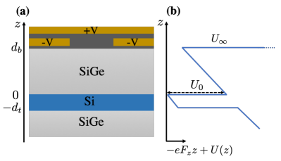
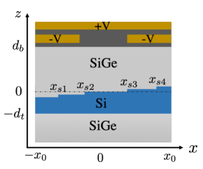
We consider a SiGe/Si/SiGe heterostructure grown along the direction while the silicon layer is between . Panel (a) of Figure 1 shows a schematic cross-section of the layer structure of the system. An electric field is applied along via the gates, and we consider both interfaces between Si and SiGe at as well as . The energy offset between the minima of the conduction band in Si and SiGe is given by meV. Moreover, we also consider the interface between the top SiGe barrier and the insulating layer that hosts the electric gates. Inside the insulating layer, we take which indicates the envelope function does not leak into that region. Panel (b) of Figure 1 shows the full potential along . Moreover, here we assume a generally elliptical quantum dot with harmonic in-plane confinement. We denote the radius of the quantum dot along by and the radius along by .
II.1 Exact envelope function in absence of a magnetic field
Within the effective mass theory and in the absence of a magnetic field, the Hamiltonian describing the envelope function reads,
| (1) |
Here and are the transverse and longitudinal effective mass, and are the confinement frequencies along and , and
| (2) |
Eq. (II.1) clearly gives rise to a separable envelope function where and are the well-known harmonic oscillator wavefunctions. Our main objective in this section is to find the exact eigenstates and eigenenergies for the out-of-plane electron motion.
Given Eq. (II.1), we write the Schrödinger equation for the envelope function as
| (3) |
We now use the electrical confinement length,
| (4) |
and its associated energy scale,
| (5) |
in order to piecewise expressing Eq. (3) as,
| (6) |
Here , and are the normalized length, eigenenergy, and potential.
The above equation, at each interval, has generally two linearly-independent solutions known as Airy functions of the first and second kind, Ai and Bi Davies . We thus find the exact solution for :
| (7) |
where we defined,
| (8) |
Note that the Bi function is omitted from the solution for . This is based on the physical ground that Bi does not give rise to a decaying behaviour inside the extended barrier layer.
In order to find the eigenenergies and determine the coefficients involved in the envelope function Eq. (7), we note that and its first derivative must be continuous at the boundaries between Si and SiGe, i.e. at and . Moreover, since there is no leakage to the insulating layer, the envelope function must vanish at . By imposing these boundary conditions, we obtain the equation below from which we can numerically find all possible eigenenergies,
| (9) |
with the definitions,
| (10) | ||||
| (11) |
and,
| (12) | |||
| (13) |
where and and are the first derivatives of the and functions.
Once the (normalized) eigenenergy is found, we use it to calculate the coefficients to . The coefficient is found by using the normalization of the envelope function. We note that by solving Eq. (II.1), we also find a set of states where the envelope function is not localized in the Si quantum well but rather in the upper SiGe barrier underneath the insulating layer. As we discuss it in Section III, the valley splitting is basically determined by the ground state localized in the Si quantum well. In the presence of a magnetic field or interface steps, we also need to take into account the excited states which have sizable overlap with the localized ground state in the Si quantum well; see Eqs. (26), (27) and (33). As such, the states that are localized underneath the insulating layer do not contribute to the behavior of the valley splitting, and we neglect them in this paper.
For the ground state of the electron motion along , we can simplify the analysis presented above and find analytic relations. As we show in Appendix A, the (normalized) ground state energy in the regime of a deep quantum well, , can be expressed up to the leading order as
| (14) |
where is the smallest root (in absolute value) of the Ai function. The normalized envelope function in this case is approximated by,
| (15) |
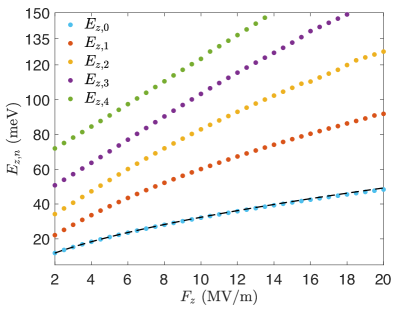
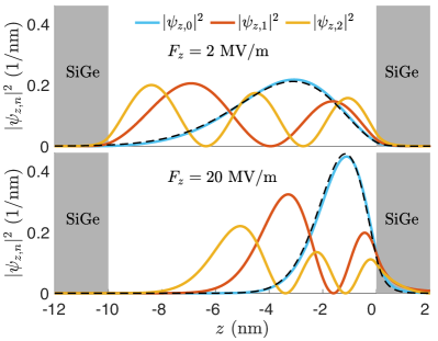
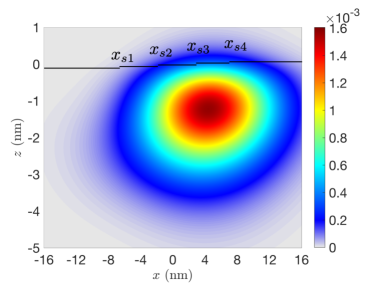
In Figure 2 we show the obtained energies for the ground state as well as first few excited states as a function of the applied electric field. In Figure 3 we also show the probability density for the ground state and first two excited states for two different electric fields. In both figures, a comparison between the numerics and the analytical relations Eqs. (14) and (15) for the ground state shows a very good agreement.
We note here that the interface-induced spin-orbit interaction is neglected in our model. Consideration of this effect has been shown to be essential for explaining the valley-dependent g-factor in silicon quantum dots Ferdous18 ; Ruskov2018 . However, as noted in Ref. Ruskov2018 , the matrix elements involved in the spin-orbit interaction are much smaller than the valley splitting matrix element. This justifies our omission of the interface-induced spin-orbit interaction. As we will show in the next sections, the information stored in the excited states enables us to obtain the full envelope function in a finite magnetic field, and also makes it possible to study realistic cases where there are steps and miscuts at the Si/SiGe interface.
II.2 Envelope function in the presence of an in-plane magnetic field with ideal Si/SiGe interface
Let us now consider a quantum dot with an ideally flat Si/SiGe interface in the presence of an in-plane magnetic field . We use a gauge for which the vector potential becomes . By substituting in Eq. (II.1), we arrive at the following form for the Hamiltonian describing the envelope function,
| (16) |
where we start from the separable Hamiltonian,
| (17) |
and treat the field-induced couplings as a perturbation,
| (18) |
We note that the confinement frequencies and lengths along and are modified by the magnetic field,
| (19) | ||||
| (20) | ||||
| (21) | ||||
| (22) |
In order to obtain the envelope function from Eq. (16), we treat exactly and apply perturbation theory in . The ground state up to the first order perturbation then reads,
| (23) |
where,
| (24) |
and,
| (25) |
where the number of relevant bound excited states in the vertical direction for is found to be , see Fig. 2. Here we defined the coefficients,
| (26) | ||||
| (27) | ||||
| (28) |
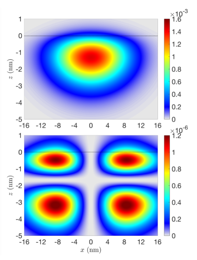
We numerically calculate and using the excited states obtained in Section 1. For a circular dot we obtain . For an elliptical dot with realistic parameters, these coefficients remain close to each other since the confinement along in quantum dots is always stronger than the in-plane confinements. Table 1 shows an example for the values of and . With the set of parameters used in Table 1, we find . Therefore, and in Eq. (II.2) are one order of magnitude larger than . In Figure 4 we show the probability density in the plane in leading order, , as well as the first order correction, .
| 1 | -9.18 | -7.15 |
|---|---|---|
| 2 | 2.85 | 2.26 |
| 3 | -1.38 | -1.10 |
II.3 Envelope function with disordered Si/SiGe interface
So far, we have studied structures where the interface between Si and SiGe is perfectly flat and is located at and . However, during the experimental fabrication of Si qubit nanostructures, the formation of miscuts and steps at the interfaces is highly probable. Such uncontrolled disorder can modify the valley splitting and its phase, and is considered to be the main reason that makes the valley splitting a device-dependent quantity. In Ref. Tariq , several configurations for the steps at the interface are considered, and in each case, the envelope function is formed from a variational ansatz that uses a smooth interpolation between the envelope functions far from the step position (i.e. envelope functions for perfect interface).
In this section, we extend our model to include stair-like interface steps parallel to the axis at the upper Si/SiGe interface as depicted in Figure 6. Our main objective here is to study how these miscuts influence the quantum dot envelope wavefunction. Note that disorder could also be present at the lower SiGe/Si interface. However, since the amplitude of the envelope function is small at the lower interface, the effects of possible disorder is negligible. We also point out that other disorder configurations at the upper Si/SiGe interface can be analyzed using the same approach.
In silicon, the thickness of each atomic layer is where nm denotes the lattice constant. This indicates that the change in the interface position due to a few miscuts is much smaller than the total thickness of the envelope function along and enables us to use perturbation theory in order to obtain the electron envelope function. We take the -position of the interface layer that contains the quantum dot center as the reference for the position of the barrier interface (e.g., the layer within in Fig. 6), and take any change to the interface position due to the miscuts as a perturbation. We describe the disordered SiGe/Si/SiGe interface with the step potential
| (29) |
where,
| (30) |
The Hamiltonian describing the envelope function with disordered interface at finite in-plane magnetic field can again be written in the form of Eq. (16) where, in this case, Eq. (II.3) is added to the perturbative part of the Hamiltonian, Eq. (18). The ground-state envelope function then reads up to the second-order perturbation with respect to the interface disorders,
| (31) |
where is a normalization constant and is the first-order correction due to the interface disorder that amounts to
| (32) |
for which the coefficients
| (33) |
shall be calculated numerically. Table 2 shows examples for the values of . Since the out-of-plane confinement is much stronger than the in-plane confinement, the largest contribution comes from and . Moreover, we observe that by taking up to 4 excited states , the values of substantially decay. As such, we can set as a cutoff in the summation in Eq. (32).
| 0 | N/A | 0.0170 | -0.0082 | 0.0047 |
|---|---|---|---|---|
| 1 | 0.4204 | -0.0564 | 0.0319 | -0.0215 |
| 2 | -0.0353 | 0.0073 | -0.0036 | 0.0019 |
| 3 | -0.0214 | 0.0069 | -0.0043 | 0.0031 |
| 4 | 0.0088 | -0.0029 | 0.0015 | -0.0008 |
| 5 | -0.0001 | -0.0001 | 0.0001 | -0.0001 |
| 6 | -0.0025 | 0.0010 | -0.0006 | 0.0003 |
| 7 | 0.0025 | -0.0012 | 0.0008 | -0.0006 |
| 8 | 0.0004 | -0.0002 | 0.0001 | 0.0000 |
For the second-order correction due to the interface disorder, we only keep the leading-order terms to arrive at (see Apendix C for more detail),
| (34) |
where the perturbative coefficients and are given by,
| (35) | ||||
| (36) |
We now take,
| (37) |
that has the same functional form as given by Eq. (32) in which the perturbative coefficients become,
| (38) |
In Figure 6, we show the electron probability density in the plane in the presence of interface steps. The asymmetry around in this case is due to the change of the quantum-dot thickness due to the interface disorder. Since in our model the Si quantum well is thicker for , the peak of the probability density is also shifted towards .
In the next section, we use the envelope functions we found in this section to study and discuss how the valley splitting of a quantum dot depends on the electric and magnetic fields for an ideally flat as well as disordered Si/SiGe interfaces.
III Discussion
Within the effective mass theory, the two low-lying valley components of the quantum dot can be written as
| (39a) | ||||
| (39b) | ||||
Here describes the Bloch wave vector of the conduction band minima and are the periodic parts of the Bloch functions for the valleys in silicon. We express these functions by a plane wave expansion,
| (40) |
for which is the reciprocal lattice vector. The coefficients in this expansion for the two valleys are related via the time-reversal symmetry relation . The wave vectors and their corresponding coefficients for Si are studied in Ref. Koiller2011 .
The valley-orbit coupling is given by,
| (41) |
Note that , and given for all practical values of (see Eq. (50)), the valley-orbit coupling is strongly dominated by the matrix element of the interface potential . Indeed, the role of the electric field is to control and shape , and the contributions from the matrix element of in the valley-orbit coupling can be neglected Koiller2011 ; Koiller2009 . The valley splitting is found from the above equation by and the valley phase can be found by
| (42) |
III.1 Electrical dependence of the valley splitting for an ideal quantum dot
In this section, we consider a quantum dot with an ideal interface in the absence of a magnetic field and use the results of Section 1 to find the electrical and interface-potential dependence of the valley splitting and the valley phase. As depicted in Figure 3, since the electric field pushes the envelope function towards the upper SiGe barrier, the probability density of the ground state at the lower SiGe/Si interface is negligible. Therefore we take and find that the valley-orbit coupling at zero magnetic field for an ideal quantum dot becomes,
| (43) |
To carry on, we note that the terms with would lead to fast oscillations in the integrand that average to zero. We therefore only consider terms with and define,
| (44) |
which we find to be using Ref. Koiller2011 .
We now take the integration by parts and find for an ideal quantum dot,
| (45) |
Here is the contribution that comes from the amplitude of at the Si/SiGe interface:
| (46) |
and is the contribution that originates from the tail of inside the barrier,
| (47) |
In order to find analytical expressions for these contributions, we use Eqs. (14) and (15) and also use the expansions given by Eqs. (69) (note that by using these equations we assume which is valid for all relevant valued for the electric field , see Eq. (50).) We finally arrive at the result
| (48) |
and
| (49) |
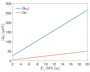
The last term in the square bracket is a number larger than (having to MV/m for a SiGe barrier, we find ). This indicates that is larger than (by nearly a factor of 6.)
We conclude that the valley-orbit coupling (and hence also the valley splitting) within the leading order scales linearly with the electric field while it is independent of the interface potential (as long as ). This linear dependence is experimentally observed in Ref. Yang2013 for a SiO2 barrier (that has a much stronger interface potential eV compared with SiGe) and it is also predicted from a theory analysis assuming that the envelope function has zero amplitude inside the barrier Ruskov2018 .
In addition to the linear-in-electric-field term, here we find the valley-splitting also has a small nonlinear dependence on the electric field (note that ). This non-linear contribution originates from the penetration of the envelope function into the barrier, and can be neglected so long as ; this holds provided,
| (50) |
For a SiGe barrier with meV, the right side of the above inequality becomes MV/m. This essentially means for all practically relevant values for , the valley splitting remains a linear function of the electric field. In Figure 7, we used Eqs. (48) and (49) and show and as a function of the electric field . The values that we show in the figure are in agreement with Refs. Culcer2012 and Koiller2009 where is reported for MV/m.
III.2 Magnetic dependence of the valley splitting for an ideal quantum dot
We now extend the results of the last section by including an in-plane magnetic field. As we have shown in Section II.2, the electron envelope function in the presence of an in-plane magnetic field includes excited states of the out-of-plane motion , see Eq. (23) and (II.2). Compared to the ground state , the excited states can have a larger amplitude at the Si/SiGe interface, and penetrate further to the barrier. As such, we generally expect that the valley splitting should increase in an in-plane magnetic field. In addition, as one can see from Figure 3, depending on the electric field, the excited states can have a sizeable amplitude at the lower SiGe/Si interface . Therefore, we take into account both upper and lower interfaces and consider a barrier potential of the form . We use Eqs. (23) and (II.2) and find for the valley-orbit coupling,
| (52) |
Using the excited states from Section 1, we numerically calculate the above integrals. The coefficients , and are introduced in Section II.2 and as we explained there, up to a few Tesla, the terms containing and are strongly dominant over the correction containing . Therefore, to the leading order, the magnetic contribution to the valley splitting scales quadratically with the magnetic field. Moreover, at finite magnetic fields, the valley splitting becomes dependent on ratio of the lateral confinement to the electrical confinement, and - see Eqs. (21) and (22).
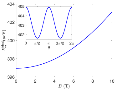
Eq. (III.2) indicates that for an elliptical quantum dot at a fixed magnetic field, the valley splitting reaches its maximal value when the direction of the magnetic field is perpendicular to the axis with the larger radius. In the main plot of Figure 8, we show the valley splitting as a function of magnetic field at a fixed direction. In the inset plot of the figure, we show the valley splitting as a function of the direction of the field. We observe that the valley splitting for a quantum dot with ideal interface only slightly increases with the magnetic field. This also indicates that the dominant contribution to the valley splitting remains a linear function of the electric field at the finite magnetic fields.
III.3 Valley splitting of a quantum dot with disordered interface
We now consider a realistic quantum dot with miscuts and steps at the Si/SiGe interface and aim to study the valley splitting and its electromagnetic dependence. We take the interface potential given by Eq. (29) and use the resulting envelope function Eq. (II.3). We then find for the valley-orbit coupling,
| (53) |
where is the valley-orbit coupling for an ideal interface given by Eq. (III.2), is the largest contribution originating from the interface disorders and reads,
| (54) |
and is a contribution that is first order with respect to and reads,
| (55) |
where,
| (56) |
The last term, , is a small and sub-leading contribution that is second-order with respect to and . More details on this term can be found in the Appendix B.
Note that in general we have and . However, as we discuss below, depending on the number and location of interface steps, can become a small number. In this case, the contribution from becomes (more) important in determining the valley splitting and its phase.
III.3.1 A single step at the interface
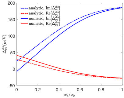
Let us now study the structure and effects of and . We begin by considering the simplest case; that is, when there is only a single step at the interface. We take the width of the step to be ; the step potential is then obtained from Eq. (II.3) by taking and . We then take to be the position of the only interface step. From Eq. (54) for a quantum dot with a single interface step we obtain,
| (57) |
In order to analyze , we note that a complete assessment of this term requires numerical calculations. However, we can obtain a rough estimation by only considering the largest contribution to Eq. (55), i.e. the term corresponding to and . For further simplicity, we also drop the second-order correction to the envelope function, , so that we take and . We then arrive at the largest contribution to due to and ,
| (58) |
in which,
| (59) |
and are clearly out of phase with . This can significantly modify and suppress the valley splitting. Note that and are monotonically decreasing if the interface step is located further away from the quantum-dot center.
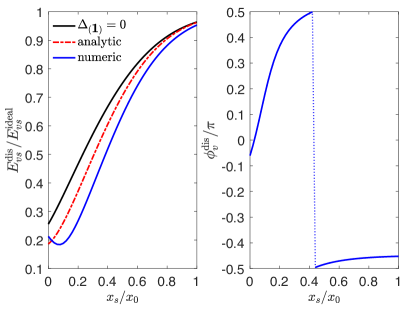
In the left panel of Figure 9 we present the normalized valley splitting as a function of the step location at . By neglecting in the valley-orbit coupling (shown in the figure by the solid black line), we observe, as predicted, that the valley splitting is monotonically decreasing as the interface step moves closer to the quantum dot center. At , the valley splitting is suppressed by 75%. This amount of suppression is reported in Ref. Tariq where a variational ansatz is used to approximate the envelope function in the presence of a single step. By taking into account the contribution (shown by the dashed-dot red line), we observe that the valley splitting only becomes further suppressed.
Remarkably, if we numerically calculate from Eq. (55) and take into account not only the dominant term corresponding to and but also the other terms as well, we observe that the valley splitting has in fact a non-monotonic behaviour as a function of the distance between the single interface step and the quantum dot center. In Appendix D, we discuss in more detail that this behaviour is due to the out-of-plane excited states .
Indeed, the terms , and are originating from the ground state of the out-of-plane motion, . As it is already shown, the closer the step to the quantum dot center, the further and suppress , until at some point, , the contributions due to the terms with in Eq. (55) reaches an equal footing as . If the interface step is placed any closer to the quantum dot center, , the latter sum continues to decrease whereas the contributions due to the terms with in Eq. (55) increase due to the increase of the coefficients . Therefore, the valley splitting begins to rise.
In the left panel of the Figure 9 we have shown the valley phase as a function of the step location. Note that the valley phase, given by Eq. (42), is a -periodic function defined within . Therefore, the sudden jump of the valley phase that occurs at can be removed by subtracting from the values above the jump.
Let us now study how the valley splitting scales with the electric and magnetic fields. As we have shown in Sec. III.1, the valley-orbit coupling for an ideal quantum dot is a linear function of the electric field. As such, the term given by Eq. (III.3.1) is also linear in electric field. However, is a non-linear function with respect to the electric field. Given Eq. (III.3.1), the dominant coefficient scales linearly with the electric field, and this gives rise to a quadratic scaling of with the electric field (more accurately, if we keep in Eq. (38), it is easy to show that acquires one more term that is cubic in the electric field.)
Therefore, in general, the valley splitting for a quantum dot with a single interface is a nonlinear function of the electric field due to the term as well as the normalization constant . In the upper panel of Figure 10, we show the valley splitting as a function of the electric field for several locations for the single interface step.
Since grows with the electric field faster than a linear function, for , we expect the valley splitting should scale sub-linearly by the electric field. The further the step is located away from the center, the smaller becomes so that the valley splitting approaches being a linear function of the electric field. For , the valley splitting is mainly determined from the terms with in . Therefore, numerical analysis is required to find the dependency of the valley splitting on the electric field.
In order to understand how the valley splitting changes with an in-plane magnetic field, we note that the confinement length is reduced by the magnetic field. Using Eqs. (21), the effect of the magnetic field to the evolution of and is equivalent as if and is located from the center at a larger distance,
| (60) |
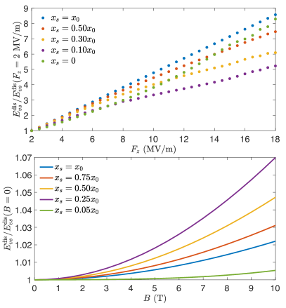
Therefore, we expect that the magnetic field should always increase the valley splitting if . Since the magnetic field effectively increases , the increase of the valley splitting by the magnetic field is larger at the step location where the slope of the curve given in the left panel of Figure 9 is steeper. For , the magnetic field decreases that controls the valley splitting. However, we observe that the valley splitting still slightly increases as a function of the magnetic field due to the increase of with the magnetic field. We display the valley splitting as a function of the in-plane magnetic field in the lower panel of Figure 10.
III.3.2 Two steps at the interface
We now consider a quantum dot with two interface steps having widths and . The step potential is then obtained from Eq. (II.3) by taking and . For further simplification, we also assume that the two steps are placed symmetrically around the center so that we can write . In this case, finding the contribution from requires numerical analysis (even only for the term with and in Eq. (55).) However, we can still obtain qualitative understanding of the behaviour of the valley splitting by only considering the effect of . In order to arrive to the extension of Eq. (54) for a quantum dot with two symmetrically located steps, we integrate over by parts, similar to Sec. III.1, and neglect the small integral containing . With this, we arrive at
| (61) |
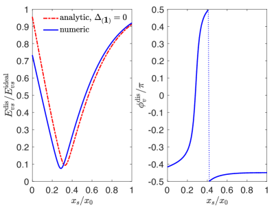
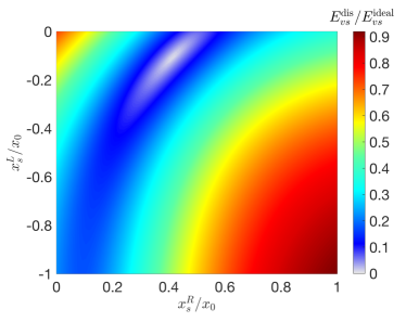
If the steps are located at the center, , we find from the above equation (taking MV/m) that is larger than in Eq. (53) (note that is largely determined by ; see Eqs. (45) and (III.2) and Fig. 7.) When the steps are located away from the center, it reduces so that eventually at some point becomes larger than . As such, we can expect that the valley splitting of a quantum dot with two symmetrically located steps is a also non-monotonic function of the steps’ location, .
This behaviour is clearly shown in the left panel of Figure 11. The dashed-dot line of the figure shows the valley splitting obtained by neglecting , using Eqs. (45), (III.2) and (III.3.2), and setting . The blue line is obtained by numerical calculation with all terms in Eq. (53) included. We observe that the effect of is to further suppress the valley splitting as well as shift the step location where the valley splitting reaches its minimum. At this step location, , the valley splitting is suppressed by more than . The right panel of the figure shows how the valley phase is changed as a function of the step location. As mentioned before, the sudden jump can be removed by using the -periodicity of the valley phase.
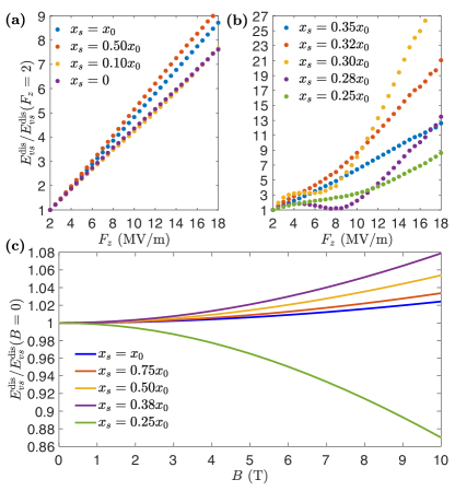
We now study the electromagnetic dependence of the valley splitting for a quantum dot with two symmetrically locates interface steps. Given Fig. 11, away from , the dominant contribution to the valley splitting is due to and . As such, we expect the scaling of the valley splitting with the electric field has to be approximately linear. This behaviour is shown in the panel (a) of the Figure 12. At the step locations close to , the contribution due to becomes important so that we can expect a strong non-linear dependency on the electric field; this is shown in the panel (b) of the Figure.
In the panel (c) of the figure we show how the valley splitting is changed by the magnetic field. For , the valley splitting is mainly controlled by . As such, since this term reduces by the magnetic field, the valley splitting is also decreasing as well. For , is the dominant contribution to the valley splitting; therefore, the magnetic field always increases the valley splitting by reducing (and .) Note that this effect is stronger for the step locations where the slope of the curve shown in left panel of Fig. 11 is steeper.
Finally, we relax the condition of the two steps being symmetric around the quantum-dot center and use the step positions and in Eq. (II.3). In Figure 13, we present our result for the normalized valley splitting as a function of the position of each step. Note that due to the non-symmetric nature of the step potential, the valley splitting turns out not to be symmetric with respect to the location of the steps. We observe that the valley splitting can completely vanish in some specific configuration of the interface steps; this is also predicted in Ref. Tariq using a simpler model. We have also studied the valley splitting for models including three and four interface steps, and we observed qualitatively similar behavior for the valley splitting as a function of electric and magnetic fields as presented in this section.
IV Summary and conclusions
To summarize, the valley splitting is one of the important properties for the silicon quantum dots that directly influences the lifetime and scalability of silicon spin qubits. As such, understanding the behaviour and tunability of the valley splitting is very important. In this work, we studied how the valley splitting responds to the electromagnetic field for both ideal and disordered quantum dots. We considered a realistic potential profile for a SiGe/Si/SiGe quantum dot by taking into account both lower and upper Si/SiGe interfaces as well the interface between upper SiGe layer and the insulating layer hosting the gate electrodes; see Fig. 1 and Eq. (2). While so far the out-of-plane electron motion has been studied by variational methods in a simpler potential model including only one Si/SiGe interface, we found the exact (within effective mass theory) envelope functions of the ground state as well as the excited states for the out-of-plane electron motion. This has enabled us to find the electron envelope function in the presence of finite magnetic field as well as interface disorder. In both cases, the envelope function reflects the coupling between in-plane to out-of-plane degrees of freedom, see Eqs. (23) and (II.3). Our analysis enables us to obtain the coupling coefficients using perturbation theory, for arbitrary configurations for the interface disorder.
We showed that in an ideal quantum dot, the valley splitting, within the leading order, always scales linearly with the out-of-plane electric field; see Fig. 7. Moreover, the valley splitting slightly increases with an applied in-plane magnetic field due to the coupling to the out-of-plane excited states; see Figure 8. The presence of interface disorder can significantly modify and suppress the valley splitting. We considered a stair-like disordered interface and studied the suppression of valley splitting due to the interface miscuts.
For a quantum dot with a disordered interface, we found that depending on the number and locations of the interface steps, the valley splitting can scale non-linearly with the electric field; see the upper panel of Figure 10 and panels (a) and (b) of Figure 12. If there is only one miscut at the interface, the magnetic field always increases the valley splitting, see the lower panel of Figure 10. However, for multiple interface miscuts, the magnetic field can both increase or even suppress the valley splitting, depending on the configuration of the miscuts, see panel (c) of Figure 12.
In the theory of spin relaxation induced by the valley coupling, one important set of quantities are the transition dipole matrix elements between the valley states Yang2013 ; Huang14 . For an ideal quantum dot, the envelope function has an in-plane mirror symmetry (Fig. 4). This, in turn, gives rise to vanishing of the in-plane dipole matrix elements. However, the presence of the interface disorder can break the in-plane mirror symmetry (Fig. 6). Our findings for the envelope function in the presence of disorder now enable the prediction of the dipole matrix elements as a function of the electromagnetic field. To our knowledge, the dipole matrix elements have always been taken as fitting parameters. Future work will be needed to further develop the theory of spin relaxation induced by the valley coupling based on a calculation of the transition dipole matrix elements and valley splitting in a magnetic field.
Acknowledgements.
We gratefully acknowledge useful discussions with Maximilian Russ and Mónica Benito. This work has been supported by ARO grant number W911NF-15-1-0149.Appendix A Ground state of a triangular potential well: A self-consistent approximation
In this appendix, we present our analysis leading to the ground state energy and wavefunction given by Eqs. (14) and (15). We first make the reasonable assumption that the ground state energy is much smaller than the interface potential . This assumption enables us to neglect the interface between the upper SiGe barrier with the insulating layer at . Moreover, since the electric field pushes the envelope function towards the upper SiGe barrier, we also neglect the lower SiGe interface at as the probability amplitude in that region is very small. Therefore, we simplify the full interface potential given by Eq. (2) for the ground state and take it as .
We can then use the confinement length and energy given by Eqs. (4)-(5) to define the dimensionless quantity,
| (62) |
We then arrive to the below Schrödinger equation for the envelope function
| (63) |
Inside the silicon layer where , is given by the Airy function of the first kind,
| (64a) | |||
Let us now consider the form of the eigenstate inside the SiGe barrier; the exact solution for the envelope function, up to prefactors, reads Ai(). However, in order to find an analytic relation for the ground state energy, we try to approximate the envelope function in the barrier. If there was no electric field inside the barrier (i.e. the term in was absent), the eigenstates would have been proportional to exp(). Due to the presence of the electric field, the potential barrier is reduced along and the wavefunction can further penetrate into the barrier. To take this into account, we introduce a parameter into the exponent of the exponentially decaying wavefunction that allows further penetration into SiGe provided . We thus approximate the wavefunction inside the barrier by,
| (64b) |
Using the continuity of the first derivative of at the interface, we can write the penetration parameter as,
| (65) |
We now self-consistently determine the ground state energy by noting,
| (66) |
From the above equation and using Eqs. (64) and (65) we finally arrive at,
| (67) |
In order to find the solution of the Eq. (A), we note that for the infinite potential well , the ground state energy is determined by the smallest root (in absolute value) of the Airy function, . This suggests that for a finite but high potential well , the solution should remain close to . As such, we consider a solution of the form,
| (68) |
and expand Ai and Ai′ functions around . We keep terms up to quadratic order in to find,
| (69a) | |||
| (69b) | |||
By substituting Eqs. (69) into Eq. (A) and keeping terms up to quadratic order we find that gives .
In order to determine which sign is physically acceptable, we note from Eqs. (64b) and (65) that the wave function decays inside the barrier provided . This is satisfied only if has a negative sign. In this case, we also find , as expected. Note that if we have kept the expansions in Eq. (69) up to the cubic order, we would have found a correction to the of order .
Appendix B Valley splitting of a disordered quantum dot in magnetic field: Higher-order terms
Appendix C Second-order correction to the envelope function due to the interface disorder
Here we present the complete form of the second order correction due to the interface steps. According to perturbation theory, we have
| (72) |
where we defined,
| (73) | |||
| (74) |
In order to arrive to Eq. (II.3), we only keep the dominant terms; i.e., in the set of , we keep , and in the set of , we keep and . Finally, in the set of , we keep .
Appendix D The effect of out-of-plane excited states in
In this appendix, we explain in more detail the effect of the excited states to the valley splitting for a quantum dot with single interface step. The step potential Eq. (II.3) in this case becomes,
| (75) |
In Section III.3, we found the contributions from and are out-of-phase with , therefore, these terms would monotonically suppress the valley splitting. Here we show that once the out-of-plane excited states are taken into account, the real part of gives rise to a non-monotonic behaviour of the valley splitting as a function of the step location, as shown in left panel of Fig. 9.
To see this effect, let us integrate Eq. (III.3) over z by parts to find,
| (76) |
where we have neglected the small contributions containing integral over and . As we have shown in Sec. III.1, the dominant contribution in is given by from Eq. (48) which is an imaginary quantity and is due to the amplitude of the envelope function at the Si/SiGe interface.
Given Eq. (D) and Eq. (55), the imaginary part of is in opposite phase with (note that in Eq. (D) we have .) Therefore, the closer the step is located to the quantum dot center, the more the imaginary part of total valley-orbit coupling is suppressed. On the other hand, the real part of the valley-orbit coupling is increased when the step is closer to the center, and at some point it becomes the dominant contribution to the total valley-orbit coupling. We plot the imaginary and real parts of the valley orbit coupling in Fig. 14. The dashed-dot lines are obtained by using the analytic relations we obtained in Sec. III.3 for and whereas the solid lines are found from numerically evaluating the valley-orbit coupling including all terms in . We observe that the non-monotonic behaviour of the valley splitting as a function of step location can be seen only by taking into account the out-of-plane excited states .
References
- (1) F. A. Zwanenburg, A. S. Dzurak, A. Morello, M. Y. Simmons, L. C. L. Hollenberg, G. Klimeck, S. Rogge, S. N. Coppersmith, and M. A. Eriksson, Rev. Mod. Phys. 85, 961 (2013).
- (2) A. Morello, J. J. Pla, F. A. Zwanenburg, K. W. Chan, K. Y. Tan, H. Huebl, M. Möttönen, C. D. Nugroho, C. Yang, J. A. van Donkelaar, A. D. C. Alves, D. N. Jamieson, C. C. Escott, L. C. L. Hollenberg, R. G. Clark, and A. S. Dzurak, Nature 467, 687 (2010).
- (3) C. H. Yang, A. Rossi, R. Ruskov, N. S. Lai, F. A. Mohiyaddin, S. Lee, C. Tahan, G. Klimeck, A. Morello and A. S. Dzurak, Nat Commun 4, 2069 (2013).
- (4) F. Borjans, D.M. Zajac, T.M. Hazard, and J.R. Petta, Phys. Rev. Applied 11, 044063 (2019).
- (5) L. V. C. Assali, H. M. Petrilli, R. B. Capaz, B. Koiller, X. Hu, and S. Das Sarma, Phys. Rev. B 83, 165301 (2011).
- (6) A. M. Tyryshkin, S. Tojo, J. J. L. Morton, H. Riemann, N. V. Abrosimov, P. Becker, H.-J. Pohl, T. Schenkel, M. L. W. Thewalt, K. M. Itoh, and S. A. Lyon, Nature Mater 11, 143–147 (2012)
- (7) M. Steger, K. Saeedi, M. L. W. Thewalt, J. J. L. Morton, H. Riemann, N. V. Abrosimov, P. Becker, and H.-J. Pohl, Science 336, 1280 (2012).
- (8) X. Mi, M. Benito, S. Putz, D. M. Zajac, J. M. Taylor, G. Burkard and J. R. Petta, Nature 555, 599–603 (2018)
- (9) N. Samkharadze, G. Zheng, N. Kalhor, D. Brousse, A. Sammak, U. C. Mendes, A. Blais, G. Scappucci and L. M. K. Vandersypen, Science 359, 1123–1127 (2018).
- (10) M. Veldhorst, J. C. C. Hwang, C. H. Yang, A. W. Leenstra, B. de Ronde, J. P. Dehollain, J. T. Muhonen, F. E. Hudson, K. M. Itoh, A. Morello and A. S. Dzurak, Nature Nanotech 9, 981–985 (2014).
- (11) J. Yoneda, K. Takeda, T. Otsuka, T. Nakajima, M. R. Delbecq, G. Allison, T. Honda, T. Kodera, S. Oda, Y. Hoshi, N. Usami, K. M. Itoh and S. Tarucha, Nature Nanotech 13, 102–106 (2018).
- (12) D. M. Zajac, A. J. Sigillito, M. Russ, F. Borjans, J. M. Taylor, G. Burkard, and J. R. Petta, Science 359, 439–442 (2018).
- (13) T. F. Watson, S. G. J. Philips, E. Kawakami, D. R. Ward, P. Scarlino, M. Veldhorst, D. E. Savage, M. G. Lagally, M. Friesen, S. N. Coppersmith, M. A. Eriksson and L. M. K. Vandersypen, Nature 555, 633–637 (2018).
- (14) W. Huang, C. H. Yang, K. W. Chan, T. Tanttu, B. Hensen, R. C. C. Leon, M. A. Fogarty, J. C. C. Hwang, F. E. Hudson, K. M. Itoh, A. Morello, A. Laucht and A. S. Dzurak Nature 569, 532–536 (2019).
- (15) L. E. Golub and E. L. Ivchenko, Phys. Rev. B 69, 115333 (2004).
- (16) M. Veldhorst, R. Ruskov, C. H. Yang, J. C. C. Hwang, F. E. Hudson, M. E. Flatté, C. Tahan, K. M. Itoh, A. Morello, and A. S. Dzurak, Phys. Rev. B 92, 201401(R) (2015).
- (17) R. Ferdous, E. Kawakami, P. Scarlino, M. P. Nowak, D. R. Ward, D. E. Savage, M. G. Lagally, S. N. Coppersmith, M. Friesen, M. A. Eriksson, L. M. K. Vandersypen and R. Rahman, npj Quantum Inf 4, 26 (2018).
- (18) P. Huang and X. Hu, Phys. Rev. B 90, 235315 (2014).
- (19) M. Friesen, S. Chutia, C. Tahan, and S. N. Coppersmith,Phys. Rev. B 75, 115318 (2007).
- (20) A. L. Saraiva, M. J. Calderón, Rodrigo B. Capaz, Xuedong Hu, S. Das Sarma, and Belita Koiller, Phys. Rev. B 84, 155320 (2011).
- (21) Y. Wu and D. Culcer, Phys. Rev. B 86, 035321 (2012).
- (22) B. Tariq and X. Hu, Phys. Rev. B 100, 125309 (2019).
- (23) R. M. Jock, N. T. Jacobson,P. Harvey-Collard, et al., Nat Commun 9, 1768 (2018).
- (24) H. J. W. Zandvliet and H. B. Elswijk,Phys. Rev. B 48, 14269 (1993).
- (25) A. Hollmann, T. Struck, V. Langrock, A. Schmidbauer, F. Schauer, K. Sawano, H. Riemann, N. V. Abrosimov, D. Bougeard, L. R. Schreiber, arXiv:1907.04146
- (26) M. Friesen, M. A. Eriksson, and S. N. Coppersmith, Appl. Phys. Lett. 89, 202106 (2006).
- (27) S. Goswami, K. A. Slinker, M. Friesen, L. M. McGuire, J. L. Truitt, C. Tahan, L. J. Klein, J. O. Chu, P. M. Mooney, D. W. van der Weide, R. Joynt, S. N. Coppersmith, M. A. Eriksson, Nature Phys 3, 41–45 (2007).
- (28) See, e.g., The physics of low-dimensional semiconductors by J. H Davies. Cambridge Univercity Press (1998).
- (29) A. L. Saraiva, M. J. Calderón, X. Hu, S. Das Sarma, and B. Koiller, Phys. Rev. B 80, 081305(R) (2009)
- (30) R. Ruskov, M. Veldhorst, A. S. Dzurak, and C. Tahan, Phys. Rev. B 98, 245424 (2018).