YBCO-based non-volatile ReRAM tested in Low Earth Orbit
Abstract
An YBCO-based test structure corresponding to the family of ReRAM devices associated with the valence change mechanism is presented. We have characterized its electrical response previous to its lift-off to a Low Earth Orbit (LEO) using standard electronics and also with the dedicated LabOSat-01 controller. Similar results were obtained in both cases.
After about 200 days at LEO on board a small satellite, electrical tests started on the memory device using the LabOSat-01 controller. We discuss the results of the first 150 tests, performed along a 433-day time interval in space. The memory device remained operational despite the hostile conditions that involved launching, lift-off vibrations, permanent thermal cycling and exposure to ionizing radiation, with doses 3 orders of magnitude greater than the usual ones on Earth. The device showed resistive switching and IV characteristics similar to those measured on Earth, although with changes that follow a smooth drift in time. A detailed study of the electrical transport mechanisms, based on previous models that indicate the existence of various conducting mechanisms through the metal-YBCO interface showed that the observed drift can be associated with a local temperature drift at the LabOSat controller, with no clear evidence that allows determining changes in the underlying microscopic factors. These results show the reliability of complex-oxide non-volatile ReRAM-based devices in order to operate under all the hostile conditions encountered in space-borne applications.
pacs:
73.40.-c, 73.40.Ns, 74.72.-hI INTRODUCTION
Many efforts have been made in recent years to deepen the study of the properties of memory devices based on the resistance switching effect (called ReRAM or Memristors), in order to analyze their possible applications as memory devices as well as in logic circuits Borghetti10 or in those that mimic the electrical behavior of synapses Jo10 or even of neurons Stoliar17 . Another area of great technological importance is related to the development of radiation resistant memories Dodd10 . This is of particular interest for aerospace industry, as electronic circuits in space must be protected from ionizing radiation from the Sun and/or from other radiation sources. Depending on spacecraft’s orbit, different strategies are employed to mitigate radiation effects Cardarilli03 ; Gerardin10 . For instance, in Low Earth Orbit (LEO) missions, long-term radiation effects, like Total Ionizing Dose (TID), is one of the main concerns. Ionizing radiation in LEO is mainly composed of high fluxes of energetic protons and electrons, trapped in the inner and outer Van Allen belts. Typically, most of this ionizing particles are stopped by aluminum shields, albeit this strategy increases spacecraft’s weight and, in consequence, mission’s cost. In the case of interplanetary or deep-space missions, main risks are transient events, like Single Event Effects, caused by high energy particles from the Sun (coronal mass ejection) or galactic cosmic rays. Usually, this missions use fail-safe systems that rely on radiation-hardened electronics, error correction algorithms and redundant CMOS circuits to mitigate this kind of effects.
Ubiquitous flash memory technology for non volatile storage relies on charge confinement, which is unstable against ionizing radiation Gerardin13 . Shielding, redundancy and watchdog timers are common strategies used to mitigate sporadic but profoundly disturbing problems triggered by the incidence of foreign radiation. At the core of the alternative ReRAM technology, memristors offer either interface or filamentary based mechanisms that rely on their constituent materials properties, thus exhibiting hardened response against ionizing radiation Velo17 . Moreover, due to their simple and downsizeable capacitor like geometry, other potential problems are expected to be tackled: robustness against launch vibrations, and stability against omnipresent thermal cycling.
The resistance switching (RS) of ReRAM devices based on perovkite oxide-metal interfaces is associated with the local valence change induced by the electric field-driven migration of oxygen vacancies Waser09a . Their electrical conduction is mainly determined by the microscopic properties of the volume of the oxide, close to the interface Fu14 ; Rosillo17 , rather than to the interfacial surface itself, as occurs for example in cases where a Schottky barrier is formed Jeong09 . This fact can be exploited to produce memory devices resistant to radiation considering that it will be more difficult for radiation to affect a volume property than one that depends solely on the surface. With this strategy in mind, in this work we explore the electrical response of YBa2Cu3O7-δ (YBCO)-based memristors at a Low Earth Orbit (LEO). The electrical tests were performed by a LabOSat-01 controller (shortly LS01 hereafter) Barella16 at a 500 km-height orbit onboard a small satellite of the Satellogic company Satellogic . The electronic controller is powered once a day: a Standard Test (ST) is carried out and the results are stored for transmission to Earth through the satellite’s communication capabilities. There is no synchronicity between this measurement and the position of the satellite, thus our results are to be analyzed as performed at random sampling at a unique LEO.
Our results indicate that the YBCO-based test structure remained operational after more than 14 months in LEO, showing similar characteristics to those previously measured on Earth. A detailed analysis of the electrical transport, based on previous models, allowed us to infer that the small drift over time observed in the electrical properties can be essentially associated with the temperature changes measured onboard the satellite at LEO and that there is no evidence of microscopic changes such as those related to the increase of defects, both by thermal cycling or ionizing radiation, that could affect the performance of the device. In that sense, our studies serve as an initial step towards the validation of perovskite oxide-based ReRAM devices for space-borne applications.
II EXPERIMENTAL DETAILS
Fully relaxed YBCO thin films were grown by pulsed laser deposition (PLD) on top of a (100) single crystal STO substrate. The deposition was performed by applying 1500 pulses with a growth rate of 0.1 nm/pulse, producing a 150 nm YBCO thick layer. This growth rate was previously confirmed by transmission electron microscopy (TEM), under the same deposition conditions Khan19 . The superconducting transition temperature ( 90 K) was determined by resistivity and magnetization measurements, confirming that the YBCO films are near optimally-doped. Additional details of their synthesis and characterization can be found elsewhere Huhtinen01 ; Paturi04 ; Peurla07 ; Khan19 .
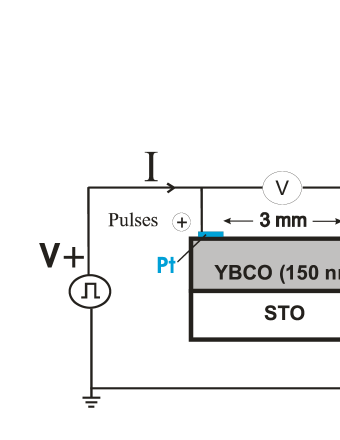
The device under test (DUT) was built by sputtering 30 nm of 2 different metal contacts (0.7 x 0.7 mm2) on top of one YBCO film surface, arranged in a planar structure (which maximizes the exposure to external irradiation), as depicted in Fig. 1. One of the contacts, labeled arbitrarily as “+”, was made with Pt, while Au was used for the ground (-) pad. We have used Pt and Au in order to produce a DUT with essentially only one active interface, as will be described later. Electrodes have a mean separation of 3 mm. Cu leads were carefully fixed over them by using silver paint without contacting directly the surface of the YBCO sample. The YBCO-based DUT was attached inside a SOIC-16 package, where its Cu leads were bonded with conductive silver paint. Finally, the package was sealed using space-qualified epoxy resin Barella18 .
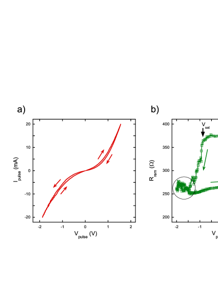
The DUT was first characterized at room temperature at the Laboratorio de Bajas Temperaturas (LBT) by using a B2902B Agilent SMU, programmed to apply 10 ms current writing pulses (Ipulse) of increasing and decreasing amplitude between 20 mA , establishing a hysteresis cycle by measuring the voltage during the pulses (Vpulse). In this way current-voltage (IV) characteristics of the DUT are measured. With 1 s delay after each writing voltage pulse, a small reading voltage is applied and again, by measuring the current, the remanent resistance (Rrem) is determined. By plotting Rrem as a function of Vpulse a resistance hysteresis switching loop (RHSL) can be observed, with Vset and Vreset as the voltages where the resistance switching begins, producing a low resistance or a high resistance state, respectively, as shown in Fig. 2. As obtained previously for ceramics Schulman13 and for thin films Lanosa20 metal/YBCO devices, our DUT exhibit a bipolar RS and hysteretical and non-linear IV characteristics. The counter-clockwise RHSL indicates that the “active” contact (ie the one that generates most of the resistance change) is, as expected, the ground Au contact, although a small change of the proper “+” device contacts is also observed (marked with circles in Fig. 2), forming the shape coined as “table with legs” Strukov08 .
To characterize the packaged-DUT in orbit, we soldered it onto a dedicated controller, the LS01 board Barella16 . This board was specifically designed to electrically test two and three terminal electronic devices in hostile environments. Its purpose is to increase the Technology Readiness Level (TRL) of electronic devices for space-borne applications. In fact, LS01 has proven to be successful characterizing TiO2-based and La1/3Ca2/3MnO3-based ReRAMs in LEO Barella19 . It uses a SMU to test the DUT and has several sensors to monitor the hostile conditions while it is operating Barella16 . Particularly, in this work, we report data from its temperature sensor and 3 solid-state dosimeters, which measure long-term radiation doses, i.e., TID using COTS pMOS transistors Lipo07 ; Inza09 ; Sanca17 . In short, when a CMOS transistor is exposed to ionizing radiation, its threshold voltage (Vth) shifts to negative values due to charge accumulation in oxide traps under the gate structure Oldham03 .
Let us now consider how LS01 performs the measurements on the DUT, while in orbit. At most once a day, the host satellite triggers a Standard Test (ST) in LS01. During a ST several experiments are run. Among them, temperature and accumulated radiation dose are registered, and IV and RHSL measurements are performed on the DUT. Although the aim was to replicate the measurements made on the DUT at LBT as accurately as possible, limitations related to the measurement platform arose. Namely, (i) the width of the current writing pulses is larger (100 ms instead of 10 ms). (ii) Only one hysteretic IV and one RHSL curve are performed per ST, as opposed to what happens at LBT where many of these curves are measured successively. This means that the relaxation-related features that emerge when considering a set of successive curves measured in orbit (sent in different STs) might look different from the features that emerge in a set of curves measured at the lab. Finally (iii), the number of writing pulse values downloaded to Earth—along with the and values needed to plot IV and RHSL curves—is smaller than the actual number of writing pulses applied to the DUT in orbit. The reason for (ii) and (iii) is that the amount of data LS01 is able to send to Earth is limited, so the available amount of data storage has to be divided among the different experiments taking place onboard. Regarding (iii), the reason the number of pulses applied and the number of pulses recorded are different, is that observing similar hysteretic behavior in different experimental setups requires replicating the same pulsing sequence in both setups. Even when LS01 is technically capable of replicating the same pulsing sequence, the amount of data generated by it might become too large to be downloaded from space. In the experiments we are about to discuss, data related to roughly 1 out of 4 pulses is recorded and sent to Earth. The pulsing sequence to measure IV and RHSL curves embedded in LS01 starts by applying a +250 A pulse, then the amplitude of the pulses is increased in steps of 250 A until it reaches a maximum of 20 mA; after that, the amplitude is decreased back to +250 A, also in 250 A steps. Once the positive part of the sequence is swept, an analog procedure is performed for the negative part, until a minimum of -17 mA is reached in steps of -250 A. 250 ms after each writing pulse is applied, a reading pulse of mA is applied. Simultaneous measurements of () are taken while applying every () pulse; these measurements are used to determine the IV and RHSL curves.
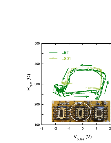
Fig. 3 depicts RHSL data acquired using the LS01 board before lift-off and using the aforementioned commercial electronics at the LBT. The inset of this figure shows the packaged YBCO-based DUT (at the center) soldered onto the board. Despite the typical variability observed in successive RHSLs, both sets of data are similar, making evident the actual sensitivity of LS01.
Next, LS01 was integrated into NuSat-5 satellite (COSPAR ID: 2018-015K) of the Satellogic company Satellogic . The rocket carrying the satellite lifted-off from Jiuquan Space Center (China) on February 5th, 2018 (day number 0 of the experiment). Once in orbit, LS01 stayed 210 days on stand-by. The first experiment over the DUT was executed on August 31st, 2018. Depending on mission task priorities, not all the ST are downloaded from space. In this way, 148 experiments executed over the DUT were downloaded, up to April 11th, 2019. This comprises a total of 433 days in orbit ( 1.2 yr).
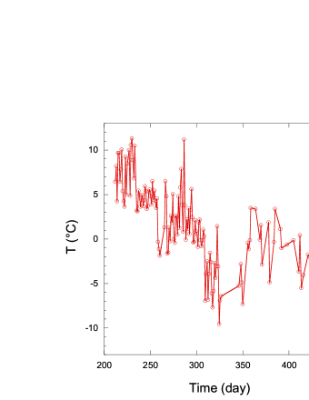
As days in orbit went by, we observed LS01’s temperature ranging mostly between -10 to 13 ∘C as can be seen in Fig. 4. Although periodic variations are expected, probably related to orbit’s cinematic ( 90 min/orbit) and to the 24 h ST execution time lapse, a smooth shift toward lower temperatures is observed as the number of days at LEO increases. Fig. 4 is a partial sample of the overall thermal cycling that is reproduced with each orbit, that may not display the maximums and minimums reached, in some cases due to repositioning of the satellite while performing other tasks.
This gives rise to additional stress on the DUT and may also affect all the associated measurement electronics.
During this period, LS01 dosimeters did not show significant threshold voltage shifts. The standard deviation of each dosimeter’s dataset was comparable to 1 Gy(Si). Nevertheless, we simulated TID using SPENVIS tool Spenvis04 to estimate expected radiation levels at the satellite orbit ( 500 km altitude).
To perform the simulations, we used the exact dates reported
above and the orbital parameters of the NuSat-5 satellite (a 500.1 km altitude circular orbit, with 97.33∘ inclination, 11.21∘ right ascension of ascending node, 251.6∘ argument of perigee, and a true anomaly of 133.3∘). Fluence and doses were simulated using an effective shielding equivalent to 9 mm-thick aluminum foam panes, AP-8 and AE-8 models for trapped protons and electrons, and ESP-PSYCHIC model for solar particles. We also consider minimum solar activity (end of Solar cycle 24), and for TID calculations we used SHIELDOSE-2 model.
The simulated differential fluences of ionizing particles found in the orbit of the satellite are shown in Fig. 5a for the total mission’s period. For energies below 10 MeV, trapped electron fluence is around 2 orders of magnitude higher than proton’s. Conversely, for higher energies, electron fluence is significantly reduced which causes that high-energy contribution to TID come mainly from trapped protons. However, this contrast in the trapped particle fluence spectra is balanced by the thick aluminum shielding and its stopping power (see Fig. 5b). As can be seen in Fig. 5c, the total TID experienced by the DUT inside the satellite is composed of similar fractions of proton and electron TID.
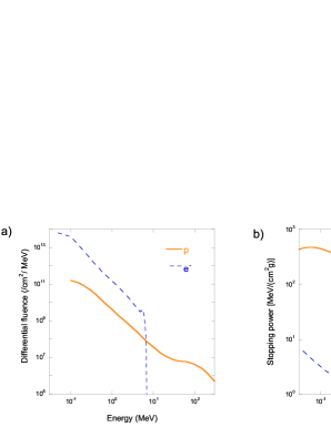
Finally, the simulations indicate that the absorbed dose should be around 2 Gy(Si) for the total mission’s period. This result is slightly lower than expected values for a 1-yr period of typical LEO missions (see references Lipo07 ; Barella19 and references therein). However, as Huston and Pfitzer pointed out Huston13 , we should consider this result as a rough approximation, as the trapped particle models used here returned overestimated predictions up to a factor of 2 in those previous works. Hence, it is not surprising that LS01 dosimeters did not sense critical levels of TID.
III RESULTS AND DISCUSSION
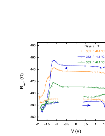
Typical successive RHSLs measured by LS01 after nearly 1 year at LEO are shown in Fig. 6. The DUT still shows bipolar resistive switching and the counter-clockwise circulation is maintained as well as the shape “Table with Legs”, indicating that the Au/YBCO interface is still the dominant with a lower resistive switching contribution of the Pt/YBCO interface. A small change in the remanent resistance can be observed after each cycle. This can be a consequence of the temperature variation of the DUT or can be related to a relaxation of the final resistance, considering the 24 h delay between successive measurements. This effect is characteristic of the YBCO-based interfaces, indicating the high mobility of oxygens along specific crystallographic orientations or in grain boundaries Schulman12 ; Placenik12 . Additionally, it can be noticed that the remanent resistance values are 15-30% higher than those measured before lift-off.
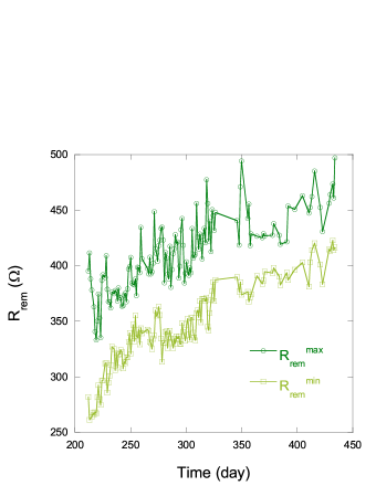
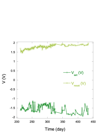
In order to gain insight on the origin of the variations observed in the RHSLs, we plotted in Fig. 7 the evolution of the maximum and minimum Rrem as a function of the days at LEO. A noisy behavior with an overall tendency to increase with increasing the number of days can be observed. A similar tendency can be observed in Fig. 8 for the voltages Vset and Vreset, although the variation of Vset with the number of days at LEO is less evident due to its noisy behavior.
In order to understand the physical origin of the observed evolution of both characteristic parameters of this memristive DUT, we can deepen our analysis trying to determine the conduction mechanisms involved in each interface. For this, we can appeal to the analysis of the IV characteristic curves based on the power exponent plotted as a function of Acha17 . Indeed, this method has been very helpful in determining the existence of different transport mechanisms present in a junction, especially when more than one is involved Acha16 ; Acevedo17 ; Ghenzi19 .
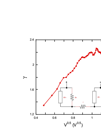
The representation of our DUT, determined before to lift-off, is shown in Fig. 9. The almost linear dependence from low voltages (with a positive intercept) and up to a voltage where a maximum is reached, confirms that a Poole-Frenkel (PF) emission is the main conduction mechanism through the interfaces of our DUT. A more detailed equivalent circuit model, which includes a leak resistor (R±) in parallel with the non-linear PF± element and a series resistor (r), representing the interface-bulk resistance plus the intrinsic resistance of the film, is presented in the inset of Fig. 9. and represent the Pt/YBCO and the Au/YBCO interfaces, respectively. This more elaborated model was determined in previous studies performed on the very same interfaces Acha11 ; Schulman15 ; Lanosa20 .
Within this framework, the current through each PF element () as a function of the voltage at a fixed temperature , can be expressed as Simmons67 :
| (1) |
with
| (2) |
where is a pre-factor associated with the geometric factor of the conducting path, the electronic drift mobility () and the density of states in the conduction band. is the trap energy level, the Boltzmann constant, the electron charge, the real part of the dielectric constant of the oxide and the interfacial thickness where most of the voltage drops (for each interface ). In this way, the voltage-dependent resistance related to the PF element of each interface can then be expressed as:
| (3) |
This equation indicates that in the low-voltage limit, the PF element behaves, as a function of temperature, as a semiconductor does. Despite the existence of the two interfaces and the parallel and serial resistances indicated in the more detailed circuit model, if we plot the measured R as a function of the temperature of each day at LEO (see Fig. 10a), we can observe that our DUT behaves as indicated by Eq. 3. In fact, this result is also indicating that the resistive behavior of the DUT is dominated by the Au/YBCO interface and more particularly by the PF emission linked to the oxide in the interfacial zone close to Au. The low resistance of both the Pt/YBCO interface (probably associated with a low R+ value) and the film intrinsic resistance (r) as well as the low ohmic conducting leakage through the R- element determine the simplicity of the obtained dependence.
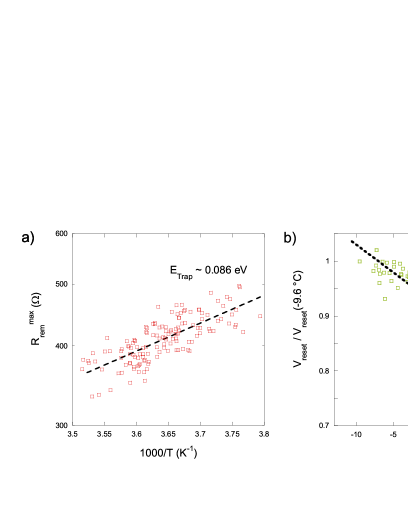
The obtained value for E is in close accordance with the values already obtained for the Au/YBCO interface in its high resistance state Schulman15 . Besides the noisy behavior of the resistance of the DUT along the days in the hostile environment at LEO, the observed drift of the remanent resistance seems to be strongly associated with the temperature variations that LS01 experiences within the satellite. This reasoning can be applied qualitatively to the high resistance state of the successive RHSLs presented in Fig. 6, where the value of R can be ordered inversely to the temperature at which the measurement was made. In a similar way, if we plot Vreset as a function of the temperature measured by LS01, the data seems to follow an almost linear dependence with a negative slope, as shown in Fig. 10b. This dependence was already observed and previously reported Acha09b .
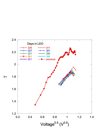
In addition to this, if we compare the curves performed by LS01 at LEO (sensing a smaller voltage range) with those performed prior to lift-off (see Fig. 11), we also obtain a result consistent with the change in temperature. This can be observed by the reduction of the slope of the linear part and by the reduction of the maximum attained, which may be attributed to the increase of the limiting series resistance (R+) as a consequence of its semiconducting-like behavior (see the similarity with Fig. 9 of reference Acha17 ). In other words, no relevant changes on the microscopic factors associated with the transport properties can be determined, other than those linked to the measured temperature variations.
IV CONCLUSIONS
A ReRAM device based on two metal-YBCO thin film interfaces was successfully tested over a period of 433 days at LEO by using the LS01 controller. The DUT remains operative after being subjected to the hostile conditions of getting into an orbit entails. Its memory characteristics are evidenced by the existence of RHSLs beside of being subjected to vibrations linked to lift-off, constant thermal cycling (C, 16x/day) and ionizing radiation representing a cumulative dose 3 orders of magnitude greater than the one it would have received for the same period of time on the surface of the Earth. Gradual changes in the electrical parameters of the ReRAM were observed (Rrem, Vset, Vreset) as the days passed in LEO. However, a detailed study of the electrical transport of the DUT revealed that there were no microscopic changes associated with the existing transport mechanisms. The observed changes could then be explained solely by taking into account the drift of the temperature to which the DUT fixed on the LS01 board was subjected. Incoming studies of the radiation effects at LEO would require the measurement of IV characteristics at constant temperature on denser micrometric arrays of perovskite oxide-metal interfaces, as well as tests over a longer period of time or under higher doses of ionizing radiation. In this way, our results represent a milestone as we move toward a next stage of testing YBCO-based devices. Future radiation dose assessment, without showing signs of malfunction or deviation from their conduction mechanism, would help to prove if perovskite oxide-based ReRAM devices perform better than other memory technologies used in satellites or spacecrafts.
V ACKNOWLEDGEMENTS
We would like to acknowledge financial support by CONICET grants PIP 11220150100322 & 11220150100653CO, ANPCyT grants PICT 2016-0966 & 2017-0984 and UBACyT grant 20020170100284BA (2018-2020). Jenny and Antti Wihuri Foundation is also acknowledged for financial support. We are indebted to Satellogic for making possible for us to perform these experiments on board of their satellites. We thank D. Giménez, E. Pérez Wodtke and D. Rodríguez Melgarejo for their technical assistance.
References
- [1] J Borghetti, G S Snider, P J Kuekes, J J Yang, D R Stewart, and R. S Williams. Memristive’ switches enable ‘stateful’ logic operations via material implication. Nature, 464:873–876, 2010.
- [2] Sung Hyun Jo, Ting Chang, Idongesit Ebong, Bhavitavya B. Bhadviya, Pinaki Mazumder, and Wei Lu. Nanoscale memristor device as synapse in neuromorphic systems. Nano Letters, 10(4):1297–1301, 2010.
- [3] Pablo Stoliar, Julien Tranchant, Benoit Corraze, Etienne Janod, Marie-Paule Besland, Federico Tesler, Marcelo Rozenberg, and Laurent Cario. A leaky-integrate-and-fire neuron analog realized with a mott insulator. Advanced Functional Materials, 27(11):1604740, 2017.
- [4] P. E. Dodd, M. R. Shaneyfelt, J. R. Schwank, and J. A. Felix. Current and future challenges in radiation effects on cmos electronics. IEEE Transactions on Nuclear Science, 57(4):1747–1763, 2010.
- [5] G. C. Cardarilli, A. Leandri, P. Marinucci, M. Ottavi, S. Pontarelli, M. Re, and A. Salsano. Design of a fault tolerant solid state mass memory. IEEE Transactions on Reliability, 52(4):476–491, 2003.
- [6] S. Gerardin and A. Paccagnella. Present and future non-volatile memories for space. IEEE Transactions on Nuclear Science, 57(6):3016–3039, 2010.
- [7] S. Gerardin, M. Bagatin, A. Paccagnella, K. Grrmann, F. Gliem, T. R. Oldham, F. Irom, and D. N. Nguyen. Radiation effects in flash memories. IEEE Transactions on Nuclear Science, 60(3):1953–1969, 2013.
- [8] Yago Gonzalez Velo, Hugh Barnaby, and Michael Kozicki. Review of radiation effects on ReRAM devices and technology. Semiconductor Science and Technology, 32(8):083002, 2017.
- [9] Rainer Waser, Regina Dittmann, Georgi Staikov, and Kristof Szot. Redox-based resistive switching memories ? nanoionic mechanisms, prospects, and challenges. Advanced Materials, 21(25?26):2632–2663, 2009.
- [10] Y. J. Fu, F. J. Xia, Y. L. Jia, C. J. Jia, J. Y. Li, X. H. Dai, G. S. Fu, B. Y. Zhu, and B. T. Liu. Bipolar resistive switching behavior of La0.5Sr0.5CoO3-σ films for nonvolatile memory applications. Applied Physics Letters, 104(22):223505, 2014.
- [11] J. C. Gonzalez-Rosillo, R. Ortega-Hernandez, J. Jareño-Cerulla, E. Miranda, J. Suñe, X. Granados, X. Obradors, A. Palau, and T. Puig. Volume resistive switching in metallic perovskite oxides driven by the metal-insulator transition. Journal of Electroceramics, 39(1):185–196, 2017.
- [12] Doo Seok Jeong, Herbert Schroeder, and Rainer Waser. Mechanism for bipolar switching in a Pt/TiO2/Pt resistive switching cell. Phys. Rev. B, 79:195317, May 2009.
- [13] M. Barella, G. A. Sanca, F. Gomez Marlasca, G. Rodríguez, D. Martelliti, L. Abanto, P. Levy, and F. Golmar. Labosat: Low cost measurement platform designed for hazardous environments. In 2016 Seventh Argentine Conference on Embedded Systems (CASE), pages 1–6, Aug 2016.
- [14] Satellogic. http://www.satellogic.com/.
- [15] M.Z. Khan, E. Rivasto, J. Tikkanen, H. Rijckaert, M. Malmivirta, M. O. Liedke, M. Butterling, A. Wagner, H. Huhtinen, I. Van Driessche, and P. Paturi. Enhanced flux pinning isotropy by tuned nanosized defect network in superconducting YBa2Cu3O6+x films. Sci Rep, 9(4):15425, 2019.
- [16] H. Huhtinen, J. Jrvinen, R. Laiho, P. Paturi, and J. Raittila. Laser deposition from a nanostructured ybacuo target: Analysis of the plume and growth kinetics of particles on SrTiO3. Journal of Applied Physics, 90(3):1521–1528, 2001.
- [17] P. Paturi, M. Peurla, K. Nilsson, and J. Raittila. Crystalline orientation and twin formation in YBCO thin films laser ablated from a nanocrystalline target. Superconductor Science and Technology, 17:564, 2004.
- [18] M. Peurla, H. Huhtinen, Y. Y. Tse, J. Raittila, and P. Paturi. Structural properties of ybco thin films deposited from different kinds of targets. IEEE Transactions on Applied Superconductivity, 17:3608–3611, 2007.
- [19] Mariano Barella. Dispositivos de memoria basados en TiO2: fabricación y caracterización en ambientes hostiles mediante un controlador dedicado (https://ri.conicet.gov.ar/handle/11336/83239). PhD thesis, Instituto Sabato, Universidad Nacional de San Martín - Comisión Nacional de Energía Atómica, March 2018.
- [20] A. Schulman and C. Acha. Cyclic electric field stress on bipolar resistive switching devices. J. Appl. Phys., 114:243706, 2013.
- [21] L F Lanosa, H Huhtinen, P Paturi, and C Acha. Electrical conduction mechanisms of metal / high-Tc superconductor (YBCO) interfaces. Journal of Physics: Condensed Matter, 32(17):175001, 2020.
- [22] D. B. Strukov, G. S. Snider, D. R. Stewart, and R. S. Williams. The missing memristor found. Nature, 453:80, 2008.
- [23] M. Barella, G. Sanca, F. Gomez Marlasca, W. Román Acevedo, D. Rubi, M.A. García Inza, P. Levy, and F. Golmar. Studying ReRAM devices at Low Earth Orbits using the LabOSat platform. Radiation Physics and Chemistry, 2019.
- [24] J. Lipovetzky, E. Gabriel Redin, and A. Faigón. Electrically Erasable Metal-Oxide-Semiconductor Dosimeters. IEEE Transactions on Nuclear Science, 54(4):1244–1250, Aug 2007.
- [25] M. G. Inza, J. Lipovetzky, E. Redin, S. Carbonetto, and A. Faigón. Stand alone MOS dosimetry system for high dose ionizing radiation. In 2009 Argentine School of Micro-Nanoelectronics, Technology and Applications, pages 27–30, 2009.
- [26] G. A. Sanca, M. Barella, F. Gómez Marlasca, G. Rodríguez, D. Martelliti, L. Patrone, P. Levy, and F. Golmar. LabOSat as a versatile payload for small satellites: first 100 days in LEO orbit. In Proceedings of the 1st Latin American Symposium of the International Academy of Astronautics on Small Satellites: Advanced Technologies and Segmented Architectures, volume 1, March 2017.
- [27] T. R. Oldham and F. B. McLean. Total ionizing dose effects in MOS oxides and devices. IEEE Transactions on Nuclear Science, 50(3):483–499, June 2003.
- [28] D. Heynderickx, B. Quaghebeur, J. Wera, E. J. Daly, and H. D. R. Evans. New radiation environment and effects models in the European Space Agency’s Space Environment Information System (SPENVIS). Space Weather, 2(10):n/a–n/a, 2004. S10S03.
- [29] S. L. Huston, G. A. Kuck, and K. A. Pfitzer. Low Altitude Trapped Radiation Model Using TIROS/NOAA Data, chapter 16, pages 119–122. American Geophysical Union, 2013.
- [30] A. Schulman, M. J. Rozenberg, and C. Acha. Anomalous time relaxation of the nonvolatile resistive state in bipolar resistive-switching oxide-based memories. Phys. Rev. B, 86:104426, 2012.
- [31] T. Plecenik, M. Tomasek, M. Belogolovskii, M. Truchl, M. Gregor, J. Noskovic, M. Zahoran, T. Roch, I. Boylo, M. Spankova, S. Chromik, P. Kus, and A. Plecenik. Effect of crystallographic anisotropy on the resistance switching phenomenon in perovskites. J. Appl. Phys., 111:056106, 2012.
- [32] C Acha. Graphical analysis of current-voltage characteristics in memristive interfaces. Journal of Applied Physics, 121(13):134502, 2017.
- [33] C. Acha, A. Schulman, M. Boudard, K. Daoudi, and T. Tsuchiya. Transport mechanism through metal-cobaltite interfaces. Applied Physics Letters, 109:011603, 2016.
- [34] W. Román Acevedo, C. Acha, M. J. Sánchez, P. Levy, and D. Rubi. Origin of multistate resistive switching in Ti/manganite/SiOx/Si heterostructures. Applied Physics Letters, 110:053501, 2017.
- [35] N Ghenzi, M Barella, D Rubi, and C Acha. Adaptive threshold in TiO2-based synapses. Journal of Physics D: Applied Physics, 52(12):125401, jan 2019.
- [36] C. Acha. Dynamical behaviour of the resistive switching in ceramic YBCO/metal interfaces. J.Phys.D: Appl.Phys., 44:345301, 2011.
- [37] A. Schulman, L. F. Lanosa, and C. Acha. Poole-frenkel effect and variable-range hopping conduction in metal/YBCO resistive switching devices. Journal of Applied Physics, 118:044511, 2015.
- [38] J. G. Simmons. Poole-frenkel effect and schottky effect in metal-insulator-metal systems. Phys. Rev., 155:657, 1967.
- [39] C. Acha. Electric pulse-induced resistive switching in ceramic interfaces. Physica B, 404:2746, 2009.