Supplemental Material for
“Anomalous Cyclotron Motion in Graphene Superlattice Cavities”
I Sample fabrication and experimental details
The presented results are based on a graphene/hBN van der Waals heterostructure. Starting with mechanically exfoliated graphene flakes from natural bulk graphite (NGS Naturgraphit GmbH) and hBN flakes from commercial hBN powder (Momentive, grade PT110), the selected single-layer graphene is then encapsulated between two hBN multilayers by sequentially piling up the three different 2D crystallites (thicknesses of top and bottom hBN are about nm and nm respectively). The crystallographic orientation of the graphene is aligned under a misorientation angle of about with respect to one of the hBN layers resulting in the formation of the moiré superlattice and the final stack is sitting on a Si/SiO2 substrate which serves as BG. The stacking procedure is done via the polymer-free assembly technique introduced in ref. Wang13, with minor adaptions (similarly to Kraft18 ).
The device is then designed with a narrow local Cr/Au TG electrode in the center of the device forming an electrostatically tunable pnp junction in combination with the overall BG. Electrical contact to the graphene is made from the edge of the mesa, where we use a single resist layer of PMMA for both etching of the graphene/hBN stack and metalization of (superconducting) Ti/Al electrodes. The self-aligned metal contacts due to utilizing the same already patterned resist for subsequent metal deposition ensure high quality electrical connection with low contact resistance. In a final step, the devices are etched into the desired shape. It needs to be said that the TG electrodes were designed and deposited first before the final etching. Thus, there is a remaining additional narrow graphene sleeve underneath the TG on the side of the device from which the electrode is launched. However, considering a wide and short junction, this issue should not conflict the presented results of this work.
The experiments were performed in a 3He/4He dilution fridge BF-LD250 from BlueFors at a temperature of about –mK, unless otherwise mentioned. Electrical measurements were conducted in a two-terminal configuration, using standard low-frequency (Hz) lock-in technique with low ac excitation (). For the electrostatic gating and source-drain biasing ultra-low noise dc-power supplies from Itest were used with an additional high power supply for the BG. All magnetic field measurements were performed in an out-of-plane magnetic field and mT were applied for the measurements at temperatures below K to suppress effects of the proximity-induced superconductivity due to the superconducting Ti/Al contacts.
II Uniform doping characteristics
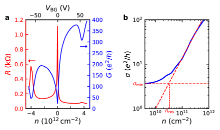
The normal graphene field effect characteristics at uniform doping are shown in Fig. S1. At maximum charge carrier density cm-2 the measured two-terminal resistance (see Fig. S1a). With the quantum resistance (where is the integer number of conductance modes and accounts for spin- and valley degeneracy) we find the contact resistance and resistivity m. The residual charge carrier density is estimated Du08 on the electron side of the primary Dirac point as cm-2 (see Fig. S1b).
III Additional cavity analysis
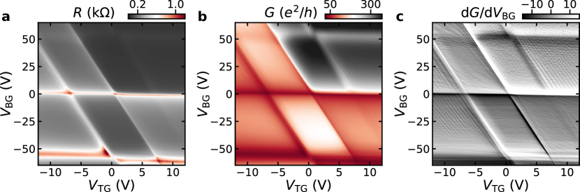
Fig. S2 displays, in turns, the raw resistance (a), conductance (b) and differentiated conductance (c) versus back gate and top gate voltages and . Charge carrier densities in the inner and outer regions of the device are converted from back gate and top gate voltages and as follows: and , where cm-2 and cm-2 are the specific gate capacitances per unit area and V and V are offset voltages of the charge neutrality point, respectively. The specific BG capacitance is determined from the Landau level fan diagram as a function of for approximately uniform doping at . The specific SG capacitance is then extracted from the lever arm of tuning the charge neutrality point with respect to the back gate .
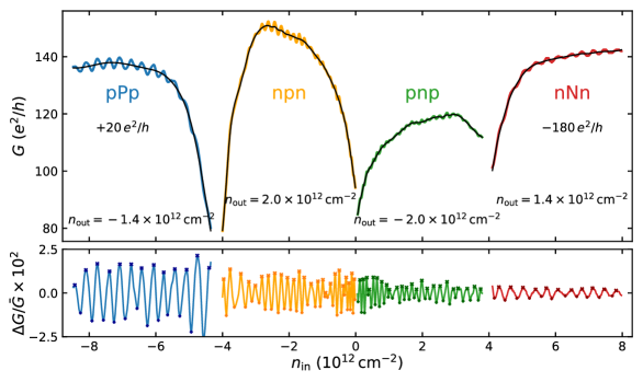
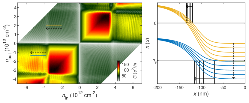
Fig. S3 displays conductance oscillations in normal and superlattice Fabry-Pérot cavities for various carrier densities of the outer regions, corresponding to the Fig.2 of the main text. As demonstrated in Handschin17 , the size of the cavity strongly varies with the top gate voltage, in particular at low charge carrier density. Fig. S4a shows quantum transport simulations of the conductance versus and . Two density profiles are extracted from Fig. S4a and plotted on Fig. S4b for various , demonstrating that the cavity size clearly shrinks passing the secondary Dirac point.
IV Additional magneto-transport: Landau level fan, Brown-Zak oscillations and Fabry-Pérot interferences
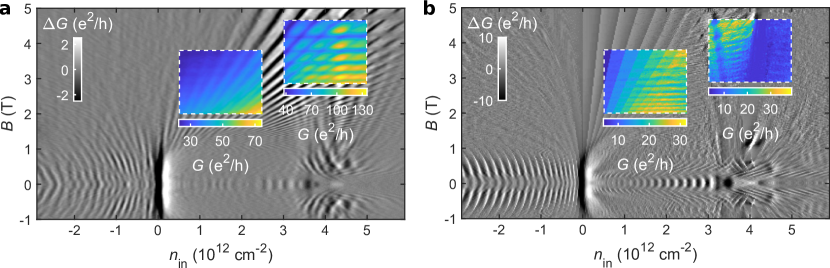
Mapping the conductance at low and medium magnetic field shows several intriguing phenomena in high quality graphene devices. Fig. S5 displays both experiment (a) and simulation (b) conductance maps, respectively, as a function of the charge carrier density and magnetic field at constant outer charge carrier density cm-2, i. e. above the electron-side secondary Dirac point in the outer reservoirs. The conductance is plotted with subtracted smooth background in the same way as Du18 . The features in the experimental map are well reproduced by our scalable tight-binding simulations Liu15 with the adapted quantum transport model for electrostatic superlattices Chen19 to our device geometry. At both primary and secondary Dirac points of the inner cavity emerging Landau level fans are observed, which are known to make up the Hofstadter butterfly spectrum at high magnetic fields Ponomarenko13 ; Dean13 ; Hunt13 . Furthermore, Brown-Zak oscillations are visible as horizontal lines in the spectrum Ponomarenko13 ; KrishnaKumar17 ; Chen17 (see colored inset panels with raw conductance in Fig. S5a and b). From the frequency of these oscillations we have determined the moiré wavelength of our superlattice structure (see below). Most notably, at low magnetic field, distinct unusual conductance oscillation patterns are observed in the junction configurations NpN and NnN, respectively (see discussion main text). The particular FP interference patterns reveal the strong sensitivity of transport through the induced electronic interferometer on the formed cavity.
V Estimation of the moiré wavelength of the superlattice structure
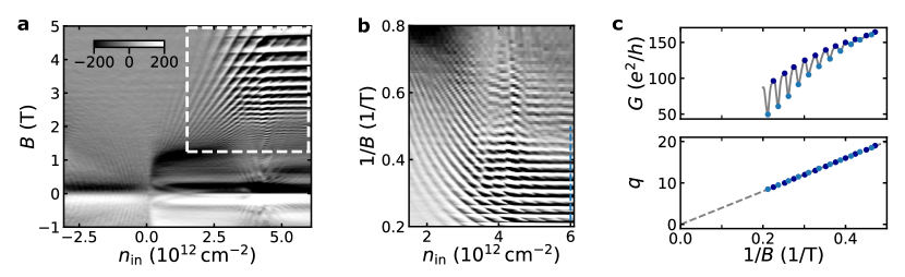
The moiré wavelength of our superlattice structure is estimated from the Brown-Zak oscillations as shown in Fig. S6. These oscillations are density independent and arise at fractional magnetic flux through the superlattice unit cell , where is the magnetic field, is the superlattice unit cell, is the magnetic flux quantum and is an integer number KrishnaKumar17 ; Chen17 . Fig. S6c (bottom panel) shows the oscillation index as a function of . From the slope of the linear fit (gray dashed line) T, we find the moiré wavelength nm. A similar value nm was used for the electrostatic superlattice potential of the quantum transport simulations, obtained as the best match for the position of the satellite Dirac points in the density-density-maps (cf. Figs. 2a, b in the main text).
VI Source-drain bias spectroscopy of Fabry-Pérot interferences
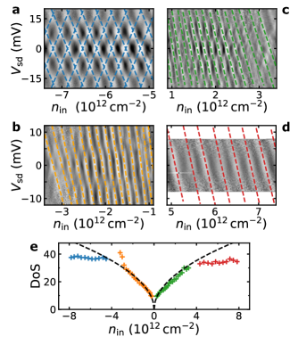
It is possible to utilize source-drain bias spectroscopy of FP interferences to probe the density of states (DoS) of the superlattice minibands within the cavity Cho11 . The four junction configurations pPp, npn, pnp and nNn are shown in Fig. S7a-d, respectively, as a function of charge carrier density and applied source-drain bias voltage . As one can see, the obtained checkerboard patterns depend on the gate conditions, i.e. the transmissions across the barriers which form the cavities Wu07 ; Pandey19 . By assuming the slope of the linearly shifted resonances to be inversely proportional to the density of states , where the change in energy is determined as , an approximate measure of the DoS can be extracted Cho11 . Fig. S7e shows the obtained values together with a theoretically expected square-root-dependence (black dashed lines) for the case of massless Dirac fermions in monolayer graphene given by , where is the Fermi velocity with eV the tight-binding hopping parameter and nm the carbon–carbon bond length. In regions npn and pnp the estimated DoS is in good agreement with the theoretical curve. We further note, that the extracted DoS features a pronounced increase when approaching the secondary Dirac point on the hole-side, which could be a signature of the van Hove singularities in the vicinity of the satellite Dirac points Indolese18 . Yet, the patterns become less clear within this range. Going beyond the secondary Dirac points where the observed FP interferences arise due to confinement of superlattice charge carriers, the DoS shows a sudden and drastic different behavior, indicative of massive particles in the superlattice minibands. However, it should be noted that the employed two-terminal measurements also include the contact resistance, which is neglected here and the voltage drop is assumed to only occur across the interferometer cavity itself. But even though a quantitative analysis is not possible for this reason, it becomes unambiguously clear that the observed patterns are distinct to the massless Dirac fermions case.
VII Fabry-Pérot interference dispersion at low magnetic field
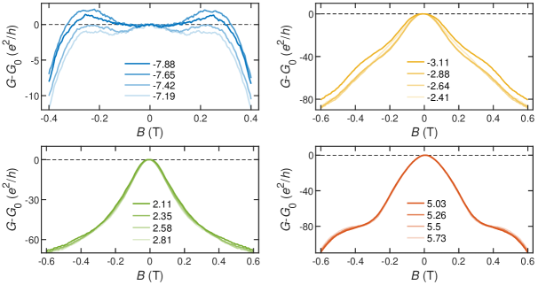
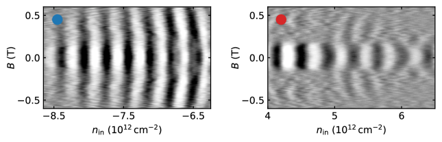
Fig. S8a shows the change in the conductance as a function of magnetic field for different at constant . The presented curves of regions npn and pnp follow the expectation of continuously reduced transparency upon applied magnetic field, which is due to the bending of trajectories and consequently larger incident angles on the barriers Shytov08 ; Young09 ; Katsnelsonbook . In contrast, pPp and nNn exhibit clearly different and more subtle behaviors as seen in Fig.3 of the main text and Fig. S9. In the pPp case, we observe a widely constant or even increased conductance at finite magnetic field before it drops, whereas in nNn the conductance features an unusual plateau-like shoulder at finite magnetic field. Noteworthy, the described anomalies in the conductance appear at the same magnetic field values where the FP interferences abruptly vanish, as discussed in the main text.
VIII Quantum transport simulations
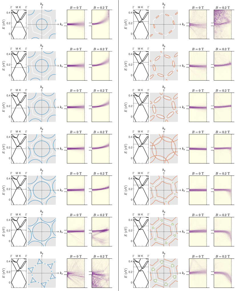
Throughout this work, all simulations are obtained from real-space Green’s function method based on a graphene lattice up-scaled by a factor of ( for Figs. S2b and 2b of the main text, which cover either high magnetic field or high density ranges, and for Figs. 3c, d of the main text, which are restricted to low magnetic field and reasonable density ranges), taking into account the scalar superlattice potential modeling the moiré pattern Yankowitz12 , as described in Ref. Chen19, . Local current densities reported in Fig. 3d of the main text are imaged by applying the Keldysh-Green’s function method in the linear response regime Cresti03 . At each lattice site , the bond charge current density is computed, where the sum runs over all the sites nearest to , is the unit vector pointing from to , and is the quantum statistical average of the bond charge current operator Nikolic06 . After computing for each site, the position-dependent current density profile is obtained, and those reported in Fig. 3d of the main text are the magnitude (see also liu17 ).
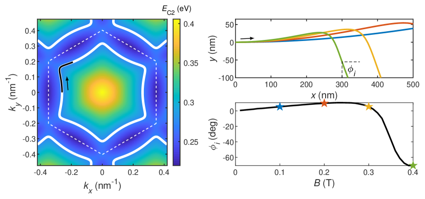
To clearly reveal the electron trajectories within the same quantum transport regime and at the same time directly connect the local current density profiles to our conductance simulations reported in Fig. 3c of the main text, we consider the same sample width of 1 m attached to a wide drain lead (also 1 m in width) at the right but a thin source lead at the left (100 nm in width). Both leads are standard graphene ribbons oriented along zigzag in the transport direction, and the moiré model potential is considered only in the central scattering region. Furthermore, the Fermi energy in the thin source lead is fixed at a low energy such that only the lowest mode with zero transverse momentum is injected. On the other hand, the Fermi energy in the wide drain lead is set to float with the attached right edge of the scattering region, in order to minimize the reflection that would blur the obtained electron beam profile. Additional beam simulations are shown in Fig. S10. Fig. S11 displays the C2 band and an example of the Fermi surface contour at an energy of 0.2728 eV as well as the calculated real space trajectories for different magnetic fields, resulting in a drastic change of the incident angle of miniband fermion trajectories onto the barrier at a critical field.
Finally, it is important to note that the experimental findings are well captured by our quantum transport simulations using a mere electrostatic superlattice potential Chen19 (but neglecting higher order terms of the moiré perturbation Wallbank15 ; Moon14 ). Our results are thus applicable to graphene miniband fermions subject to a hexagonal superlattice potential in general, such as recently demonstrated electrostatically induced superstructures in graphene Forsythe18 ; Drienovsky18 .
References
- (1) L. Wang, I. Meric, P.Y. Huang, Q. Gao, Y. Gao, H. Tran, T. Taniguchi, K. Watanabe, L.M. Campos, D.A. Muller, J. Guo, P. Kim, J. Hone, K.L. Shepard, and C.R. Dean, One-Dimensional Electrical Contact to a Two-Dimensional Material, Science 342, 614 (2013).
- (2) R. Kraft, J. Mohrmann, R. Du, P. B. Selvasundaram, M. Irfan, U. N. Kanilmaz, F. Wu, D. Beckmann, H. von Löhneysen, R. Krupke, A. Akhmerov, I. Gornyi, and R. Danneau, Tailoring supercurrent confinement in graphene bilayer weak links, Nat. Commun. 9, 1722 (2018).
- (3) X. Du, I. Skachko, A. Barker, and E.Y. Andrei, Approaching Ballistic Transport in Suspended Graphene, Nat. Nanotech. 3, 491 (2008).
- (4) C. Handschin, P. Makk, P. Rickhaus, M.-H. Liu, K. Watanabe, T. Taniguchi, K. Richter, and C. Schönenberger, Fabry-Pérot Resonances in a Graphene/hBN Moiré Superlattice, Nano Lett. 17, 328 (2017).
- (5) R. Du, M.-H. Liu, J. Mohrmann, F. Wu, R. Krupke, H. von Löhneysen, K. Richter, and R. Danneau, Tuning Anti-Klein to Klein Tunneling in Bilayer Graphene, Phys. Rev. Lett. 121, 127706 (2018).
- (6) M.-H. Liu, P. Rickhaus, P. Makk, E. Tóvári, R. Maurand, F. Tkatschenko, M. Weiss, C. Schönenberger, and K. Richter, Scalable Tight-Binding Model for Graphene, Phys. Rev. Lett. 114, 036601 (2015).
- (7) S.-C. Chen, R. Kraft, R. Danneau, K. Richter, and M.-H. Liu, Electrostatic Superlattices on Scaled Graphene Lattices, Commun. Phys. 3, 71 (2020).
- (8) L.A. Ponomarenko, R.V. Gorbachev, G.L. Yu, D.C. Elias, R. Jalil, A.A. Patel, A. Mishchenko, A.S. Mayorov, C.R. Woods, J.R. Wallbank, M. Mucha-Kruczynski, B.A. Piot, M. Potemski, I.V. Grigorieva, K.S. Novoselov, F. Guinea, V.I. Fal’ko, and A.K. Geim, Cloning of Dirac Fermions in Graphene Superlattices, Nature 497, 594 (2013).
- (9) C.R. Dean, L. Wang, P. Maher, C. Forsythe, F. Ghahari, Y. Gao, J. Katoch, M. Ishigami, P. Moon, M. Koshino, T. Taniguchi, K. Watanabe, K.L. Shepard, J. Hone, and P. Kim, Hofstadter’s Butterfly and the Fractal Quantum Hall Effect in Moiré superlattices, Nature 497, 598 (2013).
- (10) B. Hunt, J.D. Sanchez-Yamagishi, A.F. Young, M. Yankowitz, B.J. LeRoy, K. Watanabe, T. Taniguchi, P. Moon, M. Koshino, P. Jarillo-Herrero1, R.C. Ashoori, Massive Dirac Fermions and Hofstadter Butterfly in a van der Waals Heterostructure, Science 340, 1427 (2013).
- (11) R. Krishna Kumar, X. Chen, G.H. Auton, A. Mishchenko, D.A. Bandurin, S.V. Morozov, Y. Cao, E. Khestanova, M. Ben Shalom, A. V. Kretinin, K.S. Novoselov, L. Eaves, I.V. Grigorieva, L.A. Ponomarenko, V.I. Fal’ko, and A.K. Geim, High-temperature Quantum Oscillations Caused by Recurring Bloch States in Graphene Superlattices, Science 357, 181 (2017).
- (12) G. Chen, M. Sui, D. Wang, S. Wang, J. Jung, P. Moon, S. Adam, K. Watanabe, T. Taniguchi, S. Zhou, M. Koshino, G. Zhang, and Y. Zhang, Emergence of Tertiary Dirac Points in Graphene Moiré Superlattices, Nano Lett. 17, 3576 (2017).
- (13) S. Cho, and M. Fuhrer, Massless and Massive Particle-in-a-Box States in Single- and Bi-Layer Graphene, Nano Res. 4 385 (2011).
- (14) F. Wu, P. Queipo, A. Nasibulin, T. Tsuneta, T.H. Wang, E. Kauppinen, and P.J. Hakonen, Shot Noise with Interaction Effects in Single-walled Carbon Nanotubes, Phys. Rev. Lett. 99, 156803 (2007).
- (15) P. Pandey, R. Kraft, R. Krupke, D. Beckmann, and R. Danneau, Andreev Reflection in Ballistic Normal Metal/Graphene/Superconductor Junctions, Phys. Rev. B 100, 165416 (2019).
- (16) D.I. Indolese, R. Delagrange, P. Makk, J.R. Wallbank, K. Wanatabe, T. Taniguchi, and C. Schönenberger, Signatures of van Hove Singularities Probed by the Supercurrent in a Graphene-hBN Superlattice, Phys. Rev. Lett. 121, 137701 (2018).
- (17) M.I. Katsnelson, Graphene: Carbon in Two Dimensions (Cambridge University Press, 2012).
- (18) A.V. Shytov, M.S.Rudner, and L.S. Levitov, Klein Backscattering and Fabry-Pérot Interference in Graphene Heterojunctions, Phys. Rev. Lett. 101, 156804 (2008).
- (19) A.F. Young, and P. Kim, Quantum Interference and Klein Tunnelling in Graphene Heterojunctions, Nat. Phys. 5, 222 (2009).
- (20) M. Yankowitz, J. Xue, D. Cormode, J.D. Sanchez-Yamagishi, K. Watanabe, T. Taniguchi, P. Jarillo-Herrero, P. Jacquod, and B.J. LeRoy, Emergence of Superlattice Dirac Points in Graphene on Hexagonal Boron Nitride, Nat. Phys. 8, 382 (2012).
- (21) A. Cresti, R. Farchioni, G. Grosso, and G.P. Parravicini, Keldysh-Green Function Formalism for Current Profiles in Mesoscopic Systems, Phys. Rev. B 68, 075306 (2003).
- (22) B.K. Nikolić, L.P. Zarbo, and S. Souma, Imaging Mesoscopic Spin Hall Flow: Spatial Distribution of Local Spin Currents and Spin Densities in and out of Multiterminal Spin-Orbit Coupled Semiconductor Nanostructures, Phys. Rev. B 73, 075303 (2006).
- (23) M.-H. Liu, C. Gorini, and K. Richter, Creating and Steering Highly Directional Electron Beams in Graphene, Phys. Rev. Lett. 118, 066801 (2017).
- (24) P. Moon, and M. Koshino, Electronic Properties of Graphene/Hexagonal-Boron-Nitride Moiré Superlattice, Phys. Rev. B 90, 155406 (2014).
- (25) J.R. Wallbank, M. Mucha-Kruczyński, and V.I. Fal’ko, Moiré Superlattice Effects in Graphene/Boron-Nitride van der Waals Heterostructures, Ann. Phys. 527, 359 (2015).
- (26) C. Forsythe, X. Zhou, K. Watanabe, T. Taniguchi, A. Pasupathy, P. Moon, M. Koshino, P. Kim, and C.R. Dean, Band Structure Engineering of 2D Materials Using Patterned Dielectric Superlattices, Nat. Nanotech. 13, 566 (2018).
- (27) M. Drienovsky, J. Joachimsmeyer, A. Sandner, M.-H. Liu, T. Taniguchi, K. Watanabe, K. Richter, D. Weiss, and J. Eroms, Commensurability Oscillations in One-Dimensional Graphene Superlattices, Phys. Rev. Lett. 121, 026806 (2018).
- (28) N.W. Ashcroft, and N. D. Mermin, Solid State Physics (Holt, Rinehart and Winston, New York, 1977).