Plumbene on a magnetic substrate: a combined STM and DFT study
Abstract
As heavy analog of graphene, plumbene is a two-dimensional material with strong spin-orbit coupling effects. Using scanning tunneling microscopy (STM), we observe that Pb forms a flat honeycomb lattice on an Fe monolayer on Ir(111). In contrast, without the Fe layer, a structure of Pb on Ir(111) is found. We use density functional theory (DFT) calculations to rationalize these findings and analyze the impact of the hybridization on the plumbene band structure. In the unoccupied states the splitting of the Dirac cone by spin-orbit interaction is clearly observed while in the occupied states of the freestanding plumbene we find a band inversion that leads to the formation of a topologically non-trivial gap. Exchange splitting as mediated by the strong hybridization with the Fe layer drives a quantum spin Hall to quantum anomalous Hall state transition.
Since the exotic properties of graphene have been discovered about 15 years ago Novoselov et al. (2004), the field of two-dimensional materials in general and honeycomb structures in particular has seen a dramatic increase in popularity Castro Neto et al. (2009). Topological properties in these lattices depend significantly on the strength of spin-orbit coupling (SOC) effects that are notoriously small in graphene, especially at the point Liu et al. (2011). Therefore, although the quantum spin Hall effect (QSHE) was first theoretically predicted for graphene Kane and Mele (2005), experimentally it was first verified in materials containing heavy elements like HgTe quantum wells König et al. (2007). Since then, numerous studies have focused on the synthesis and properties of heavier analogs of graphene like silicene Molle et al. (2018), germanene Zhang et al. (2016) or stanene (Sn) Zhu et al. (2015). But the formation of double bonds in this series seems to be restricted to the carbon-based material only and freestanding heavier analogs are considered unlikely to form Hoffmann (2013). Consequently, the first silicene was reported as adlayer on Ag(111) Vogt et al. (2012) and it is still challenging to balance the interaction with the substrate required for formation with the electronic independence necessary to study the topological properties via electronic transport effects Molle et al. (2018). Furthermore, all heavier analogs of graphene have a tendency to pronounced buckling of their honeycomb structures, resulting in severe changes of the electronic properties as compared to the ideal flat structures Huang et al. (2014). Therefore, it came recently as a welcome surprise that stanene was observed to grow on Cu(111) as a flat honeycomb lattice Deng et al. (2018). Despite the metallic substrate, a topological edge state could be observed on these islands - although 1.3 eV below the Fermi level.
In this quest for heavy honeycomb structures the Pb analog, plumbene, appeared relatively late on the scientific stage. Isoelectronic in its valence shell with C, Si, Ge and Sn it is the heaviest graphene analog and expected to show the most pronounced SOC effects Huang et al. (2014). Density functional theory (DFT) studies of plumbene predicted the formation of a buckled honeycomb structure but without band inversion near the Fermi level Yu et al. (2017). Electronically it is similar to a Bi(111) bilayer with less electrons (, ). DFT studies suggested that doping or chemical modification of plumbene Zhao et al. (2016) might be necessary to achieve topological effects. Maybe it is because of these findings that the quest for plumbene has not really started yet.
Using scanning tunneling microscopy (STM) and DFT we show in this Letter that (i) using an appropriate substrate it is possible to form a flat plumbene lattice and (ii) that the electronic properties of ’flat plumbene’ are rather exciting: Calculations predict a band-inversion in the valence bands that leads to topologically protected edge states. Further (iii), on the ferromagnetic substrate that enables the formation of plumbene the induced exchange splitting drives this feature into a quantum anomalous Hall gap. Such exchange coupling opens the way to realize a quantum Hall effect without external magnetic field, a phenomenon envisioned theoretically in the eighties Haldane (1988) and only recently realized experimentally Chang et al. (2013) at very low temperatures.
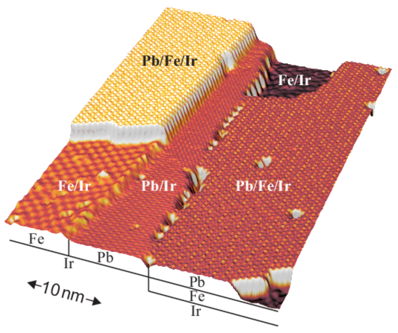
We have deposited sub-monolayer amounts of Pb onto a sample with extended Fe monolayer areas on an Ir(111) single crystal surface, see overview STM image in Fig. 1. Because we observed severe intermixing of Pb and Fe for Pb growth at room temperature we have cooled the Fe/Ir(111) to about K prior to the Pb deposition Sassmannshausen et al. (2018), which results in large and well-ordered patches of Pb both on the bare Ir(111) and the Fe-covered Ir(111), see labels for the different layers in Fig. 1. The Fe monolayer grows pseudomorphically in fcc stacking on the Ir(111) substrate and in this spin-polarized STM measurement Wiesendanger (2009) the observed roughly square superstructure with a periodicity of about 1 nm originates from the magnetic nanoskyrmion lattice Heinze et al. (2011). No magnetic signal has been observed on the Pb monolayers.
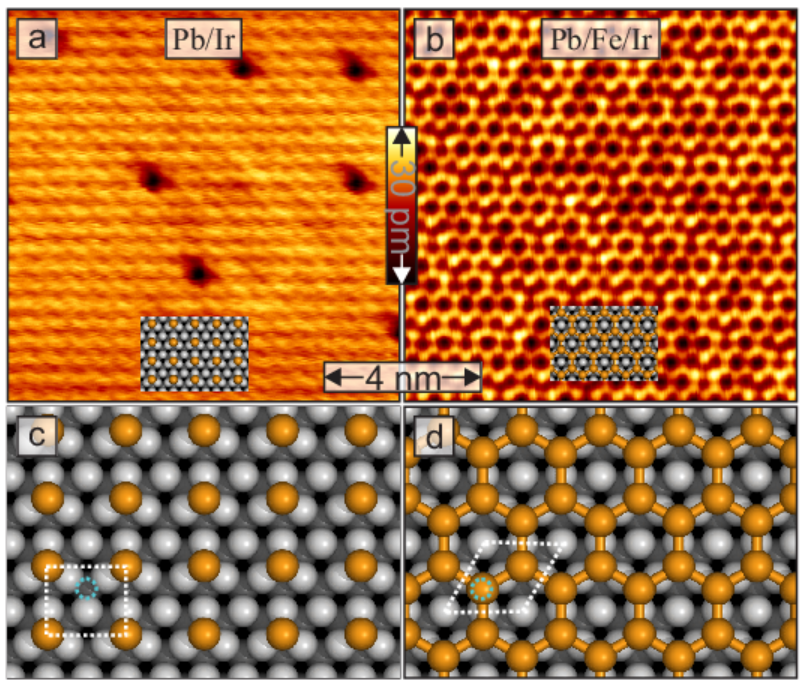
A closer view on the Pb deposited directly on the Ir and on Fe/Ir is shown in Figs. 2(a) and (b), respectively. Here the superstructures are of structural origin. Due to the large lattice mismatch of Pb and Ir, the Pb overlayers are not pseudomorphic, but instead form layers with reduced atom density. Nevertheless, the Pb superstructures are commensurate with the substrate and atoms reside at specific adsorption sites of the Ir or Fe/Ir, an indication that the Pb-substrate interaction is comparable to the Pb-Pb interaction.
On Ir(111) we find a Pb overlayer that can be described with a rectangular unit cell, see white dashed rectangle in Fig. 2(c), like in the graphene intercalated Pb films on Ir Calleja et al. (2015). The Pb atoms all occupy the same adsorption sites and the Pb-Pb distances are 4.70 Å and 5.43 Å for the two orthogonal directions. For symmetry reasons three rotational domains are found on a larger scale.
In contrast, on the Pb/Fe/Ir we find a honeycomb arrangement of the Pb atoms, see experimental data and corresponding structure model in Figs. 2(b),(d), i.e. the Pb grows on Fe/Ir(111) in the modification of plumbene. The structural unit cell (see white dashed diamond) contains two Pb atoms that adsorb in a fcc and a hcp site. The Pb atom density of this honeycomb plumbene layer is twice that of the Pb overlayer on Ir. Since both the Fe/Ir and the Ir(111) surface have the same symmetry and identical atomic distances, the difference in the Pb overlayer structures cannot originate from geometrical reasons. While the structural unit cell of the honeycomb has lattice vectors with a length of 5.43 Å, the Pb-Pb distance is only Å, i.e. more than 10% shorter than in fcc Pb ( Å). Comparing graphene with diamond a similar contraction of bond distances (1.42 Å vs. 1.55 Å) can be observed, suggesting that the Pb-Pb bond is modified in a similar way as the C-C bond for the two different allotropes.
Using density functional theory we study the energetics of different Pb monolayers on Ir(111) and Fe/Ir(111). Based on the experimental findings we compare four possible arrangements of Pb at these surfaces: and unit cells (uc.) with one or two Pb atoms per cell, i.e. the structures shown in Figs. 2(c) and (d) with and without the atoms at positions marked by the dashed blue circle.
Comparing fcc and hcp adsorption sites, a single Pb atom on Ir(111) forming a or structure always prefers the fcc site by 49 meV/Pb. The and arrangements differ by only 5 meV in favor of the former. The fact that experimentally a structure is observed might be related to neglected effects from the vibrational entropy or limitations of the computational method. To put two Pb atoms into a uc., however, requires 54 meV/Pb more energy than a single one and the formation of a Pb honeycomb lattice in the cell is energetically 216 meV/Pb more expensive than the arrangement with the same atom density. Thus, on Ir(111) a low Pb atom density with larger Pb-Pb distances is energetically favorable as found in the experiments reported here and in the graphene covered system Calleja et al. (2015). Our STM simulations based on the local density of states (LDOS) also show good agreement with the experimental images (see supplementary information, Fig. S2).
This high energy cost to form a Pb honeycomb structure on Ir(111) is contrasted by the energetics of Pb on Fe/Ir(111): here the honeycomb lattice is favored by 11 meV/Pb atom over the structure with the same areal Pb density (2 Pb/uc.) and by 44 meV over a arrangement with only one Pb atom per unit cell. The structural relaxation shows that the honeycomb layer is almost completely flat with a corrugation of 0.002 Å. In all cases we assumed a ferromagnetic order of the Fe layer. Test calculations of Fe layers with antiferromagnetic nearest neighbor interactions lead to much higher total energies (see supplementary information). A similar magnetic hardening was observed when coronene is adsorbed on the Fe/Ir(111) nanoskyrmion lattice Brede et al. (2014) and can occur generally, when electrons of molecules interact with a magnetic layer underneath Friedrich et al. (2015).
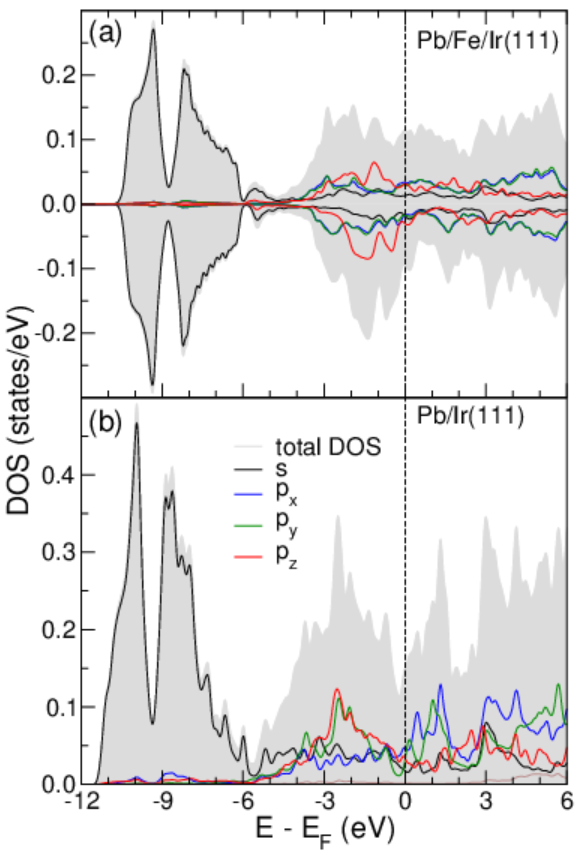
To understand the radically different energetics of Pb on Ir(111) and on Fe/Ir(111) we analyze the orbitally resolved density of states (DOS) for the honeycomb structure in Fig. 3. In the case of the Fe/Ir(111) substrate, we see that the DOS of the Pb and states is almost degenerate and rather featureless near the Fermi level, while the states show characteristic peaks at or below 1 eV binding energy where the minority Fe states are located (the majority states of Fe are peaked between 2 and 3 eV binding energy, see supplementary information, Fig. S3). While in this case the in-plane and out-of-plane oriented orbitals of Pb seem rather decoupled (as expected from a 2D structure bonded by orbitals to the substrate), in the Pb/Ir(111) case we find a completely different orbital arrangement with / orbitals bonding to the Ir substrate. Although also in this case an almost flat Pb honeycomb structure is obtained, the involved orbitals are completely different. Therefore, it can be concluded that the hybridization with the Fe states, that are available in the energy range of the Pb states, is responsible for the formation of the 2D Pb honeycomb lattice.
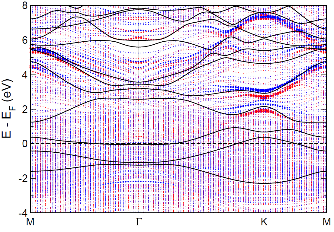
Turning now to the band structure of Pb on Fe/Ir(111), it is instructive to investigate first the plumbene layer without the substrate (black lines in Fig. 4). Below the Fermi level two rather flat bands can be found and the states form a hole pocket around the point, compensated by a shallow electron pocket of the antibonding states at . At around 1 eV binding energy the bonding states show a band inversion with the states at the point, very similar to the band inversion observed for stanene in Ref. Deng et al. (2018). On the metallic substrate these Pb states are, however, strongly hybridized with the Fe states and –as evident from Fig. 4– only above the Fermi level the individual Pb states can be identified again. The induced spin-splitting in these states is substantial, between 0.2 and 0.4 eV. This can be seen best at the point, where the Dirac-type band crossing is lifted by SOC (for the band structure without SOC see supplementary information, Fig. S4.
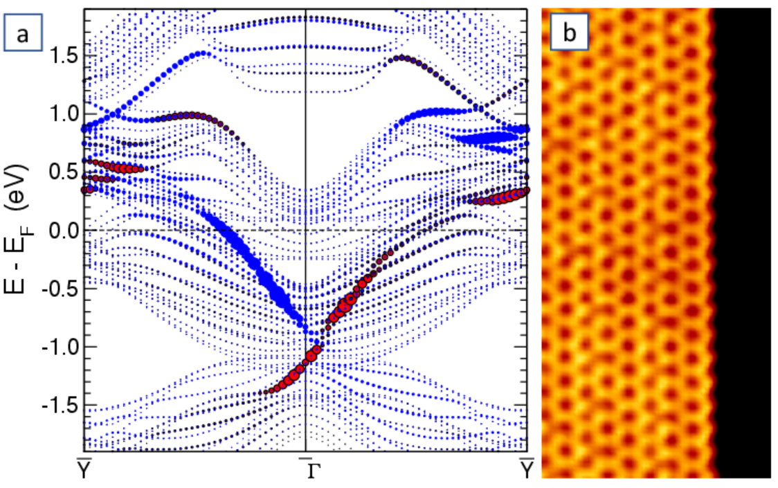
Although the features of the Pb bands are blurred by hybridization, it is of interest to study the consequences of the above-mentioned band inversion of plumbene at the point. Strong SOC in Pb opens a 150 meV band gap between the states that hosts topologically protected edge states. In the calculation of the edge-hydrogenated plumbene zig-zag ribbon the linear dispersion of the edge state is clearly visible in the gap (see supplementary information, Fig. S5). This is a clear signature of the quantum spin Hall effect (although in the occupied states) as expected from the parity analysis of the bands. Since the Fe substrate induces a strong exchange field in the plumbene, we can further look for the appearance of a quantum anomalous Hall gap in the system. To simulate the effect of the exchange field in the unsupported plumbene ribbon, we add an external magnetic field in the calculation that reproduces the spin-splitting of the Pb bands seen in Fig. 4. Although in the projection on the edge the spin-split band-edges now overlap, the single, spin-polarized edge channel is clearly visible in this system (Fig. 5).
We have shown experimental and theoretical evidence that the heaviest member of the graphene family, plumbene, can be prepared on an Fe layer on Ir(111). Selective hybridization of the Pb states with the Fe minority states stabilize the honeycomb structure, while on bare Ir(111) a rectangular Pb layer is formed. The ferromagnetic substrate induces a significant exchange splitting in the plumbene. Freestanding plumbene with this lattice constant shows a band-inversion in the occupied states and topologically protected edge states. With the exchange splitting this quantum-spin-Hall gap is changed into a quantum-anomalous-Hall gap providing a protected charge channel. Although on the metallic substrate these states will be considerably broadened and not accessible to transport measurements, with a modified substrate this system might be a nice platform to study the properties of edge states of a Chern insulator.
Acknowledgments
We would like to thank Niklas Romming for technical assistance with the experiments. We gratefully acknowledge the Collaborative Research Center SPP 1666 of the Deutsche Forschungsgemeinschaft (DFG) and the computing time on the JURECA supercomputer of the Jülich Supercomputing Centre (JSC). Financial support from the ERC Advanced Grant ADMIRE is gratefully acknowledged.
References
- Novoselov et al. (2004) K. S. Novoselov, A. K. Geim, S. V. Morozov, D. Jiang, Y. Zhang, S. V. Dubonos, I. V. Grigorieva, and A. A. Firsov, Science 306, 666 (2004).
- Castro Neto et al. (2009) A. H. Castro Neto, F. Guinea, N. M. R. Peres, K. S. Novoselov, and A. K. Geim, Rev. Mod. Phys. 81, 109 (2009).
- Liu et al. (2011) C.-C. Liu, W. Feng, and Y. Yao, Phys. Rev. Lett. 107, 076802 (2011).
- Kane and Mele (2005) C. L. Kane and E. J. Mele, Phys. Rev. Lett. 95, 226801 (2005).
- König et al. (2007) M. König, S. Wiedmann, C. Brüne, A. Roth, H. Buhmann, L. W. Molenkamp, X.-L. Qi, and S.-C. Zhang, Science 318, 766 (2007).
- Molle et al. (2018) A. Molle, C. Grazianetti, L. Tao, D. Taneja, M. H. Alam, and D. Akinwande, Chem. Soc. Rev. 47, 6370 (2018).
- Zhang et al. (2016) L. Zhang, P. Bampoulis, A. N. Rudenko, Q. Yao, A. van Houselt, B. Poelsema, M. I. Katsnelson, and H. J. W. Zandvliet, Phys. Rev. Lett. 116, 256804 (2016).
- Zhu et al. (2015) F.-F. Zhu, W.-J. Chen, Y. Xu, C.-L. Gao, D.-D. Guan, C.-H. Liu, D. Qian, S.-C. Zhang, and J.-F. Jia, Nature Mater. 14, 1020 (2015).
- Hoffmann (2013) R. Hoffmann, Angew. Chem. Int. Ed. 52, 93 (2013).
- Vogt et al. (2012) P. Vogt, P. De Padova, C. Quaresima, J. Avila, E. Frantzeskakis, M. C. Asensio, A. Resta, B. Ealet, and G. Le Lay, Phys. Rev. Lett. 108, 155501 (2012).
- Huang et al. (2014) Z.-Q. Huang, C.-H. Hsu, F.-C. Chuang, Y.-T. Liu, H. Lin, W.-S. Su, V. Ozolins, and A. Bansil, New Journal of Physics 16, 105018 (2014).
- Deng et al. (2018) J. Deng, B. Xia, X. Ma, H. Chen, H. Shan, X. Zhai, B. Li, A. Zhao, Y. Xu, W. Duan, S.-C. Zhang, B. Wang, and J. G. Hou, Nature Mater. 17, 1081 (2018).
- Yu et al. (2017) X.-L. Yu, L. Huang, and J. Wu, Phys. Rev. B 95, 125113 (2017).
- Zhao et al. (2016) H. Zhao, C.-W. Zhang, W.-X. Ji, R.-W. Zhang, S.-S. Li, S.-S. Yan, B.-M. Zhang, P. Li, and P.-J. Wang, Sci. Reports 6, 20152 (2016).
- Haldane (1988) F. D. M. Haldane, Phys. Rev. Lett. 61, 2015 (1988).
- Chang et al. (2013) C.-Z. Chang, J. Zhang, X. Feng, J. Shen, Z. Zhang, M. Guo, K. Li, Y. Ou, P. Wei, L.-L. Wang, Z.-Q. Ji, Y. Feng, S. Ji, X. Chen, J. Jia, X. Dai, Z. Fang, S.-C. Zhang, K. He, Y. Wang, L. Lu, X.-C. Ma, and Q.-K. Xue, Science 340, 167 (2013).
- Sassmannshausen et al. (2018) J. Sassmannshausen, A. Kubetzka, P.-J. Hsu, K. von Bergmann, and R. Wiesendanger, Phys. Rev. B 98, 144443 (2018).
- Wiesendanger (2009) R. Wiesendanger, Rev. Mod. Phys. 81, 1495 (2009).
- Heinze et al. (2011) S. Heinze, K. von Bergmann, M. Menzel, J. Brede, A. Kubetzka, R. Wiesendanger, G. Bihlmayer, and S. Blügel, Nature Phys. 7, 713 (2011).
- Calleja et al. (2015) F. Calleja, H. Ochoa, M. Garnica, S. Barja, J. J. Navarro, A. Black, M. M. Otrokov, E. V. Chulkov, A. Arnau, A. L. V. de Parga, F. Guinea, and R. Miranda, Nature Phys. 11, 43 (2015).
- Brede et al. (2014) J. Brede, N. Atodiresei, V. Caciuc, M. Bazarnik, A. Al-Zubi, S. Blügel, and R. Wiesendanger, Nature Nanotechnology 9, 1018 (2014).
- Friedrich et al. (2015) R. Friedrich, V. Caciuc, N. S. Kiselev, N. Atodiresei, and S. Blügel, Phys. Rev. B 91, 115432 (2015).