Phase Change Material Photonics
1 Introduction
In the last decade phase change materials (PCM) research has switched from practical application in optical data storage toward electrical phase change random access memory technologies (PCRAM). As these devices are commercialised, we expect the research direction to switch once again toward electrical-photonic devices.
When phase change material devices are heated using nanosecond pulses, the material can be SET into the crystal state, and RESET into the amorphous state, which changes the electrical resistivity by orders of magnitude and radically changes the PCM optical constants. It is this optical change that is exploited in phase change photonics. The objective of this chapter is to introduce the concepts in PCM-tuned photonics. We will start by reviewing the key works in the field, before concentrating on Metal-Dielectric-Metal (MDM) structures. We will discuss how to design tuneable-MDM photonics devices, their advantages, and their limitations. Finally we will discuss new materials for phase change photonics.
1.1 Motivation
The properties of traditional optical materials, such as glasses, are usually fixed. Therefore, the only way to change the behaviour of optical devices composed from these fixed optical materials is by precisely altering the device geometry. Since the wavelength of light is sub-micron, the geometry of these optical structures must be precisely controlled, which makes tuneable optical systems expensive. However, more modern materials with tuneable optical properties, such as liquid crystals, electrochromics, and phase change materials can be used to control the propagation of light in a structure with a fixed geometry. Fixing the geometry of a tuneable optical system reduces its complexity and should lower the manufacturing cost. Applications of tuneable photonics include telecommunications, displays, optical computing, and sensing, which employ tuneable monochromators, modulators, and lenses. Clearly, reducing the manufacturing cost of these devices will also make these technologies more affordable to the end users.
Liquid crystals and electrochromic materials tend to exhibit a rather small change in their optical constants when switched. Moreover, their switching speed tends to be at best tens of microseconds, and when the switching energy source is removed, these materials revert back to their default optical state. I.e. they are ‘momentary’ switches. In contrast, phase change materials can switch on a sub-nanosecond time scale[41, 24], and their optical state is non-volatile. They retain their optical state even when no energy is supplied. I.e. they are ’latch’ switches. This makes phase change materials particularly attractive for low energy optical devices that need to be switched quickly.
2 Background
The application of PCMs to optics and photonics was limited to optical data storage until the advent of nanophotonics in the 2000s. Nanophotonics requires only small quantities of tuneable material to control the properties of the nanoscale optical structures. This is important because the energy used to thermally switch PCMs decreases with volume[29]. From a thermal design perspective, the smaller the volume of PCM, the easier it is to quench at the rates necessary for re-amorphisation, which is required for reversible switching.
In 2006, Strand et al used simulations to demonstrate the potential of phase change data storage materials for tuning the properties of nanophotonic devices[39]. Two very different devices were simulated: (1) a switchable photonic crystal add-drop multiplexer, and (2) a reflective phase array. Both devices were designed to operate at a wavelength of 1550 nm, which is at the center of the telecoms C-band. The photonic crystal consisted of arrays of holes drilled into the high refractive index PCM. The optimum design employed a 225 nm phase change layer with arrays of holes that were also 225 nm in diameter. The beam steering phase array required repeating cells which were 500 nm wide squares. Each cell was then sub-divided into a 7-by-7 array or PCM pillars. Therefore, the largest pillar had a diameter of 71.5 nm. These features are, therefore, an order of magnitude smaller than the wavelength of light. Accurately patterning these periodic structures over a large area is extremely challenging. Indeed, the Ge2Sb2Te5 -based all-dielectrics phase array beam steering devices were only demonstrated in 2019, some 16 years after the simulation paper[14], whilst the PCM photonic crystal add-drop mulitplexer has not yet been demonstrated.
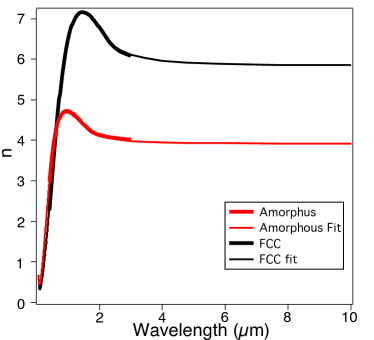
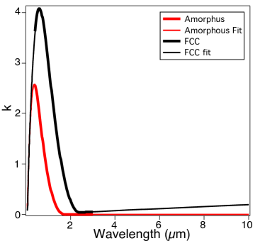
Strand et al. also realised that the conventional phase change data storage materials along the Sb2Te3–GeTe pseudo-binary tie-line have a high optical absorption at telecommunications wavelengths. Figure 1 shows the complex refractive index of Ge2Sb2Te5. As can be seen, the extinction coefficient, k, which is related to optical absorption, is large for wavelengths shorter than 2000 nm. Since Strand’s devices need to be non-lossy, the PCM must have an absorption lower than Ge2Sb2Te5. To achieve this they alloyed small amounts of unnamed elements with Ge2Sb2Te5 to lower k below 0.01 at a wavelength of 1550 nm[39]. The high optical absorption of phase change materials is a key problem that needs to be overcome for PCM photonics to have real practical applications. We will discuss this further in section 5.
The current phase change photonics research landscape can be split into three themes: (1) On-chip photonics, (2) Metasurfaces, and (3) Materials Engineering. It is interesting that these three themes were all addressed in the seminal simulations by Strand et al[39].
The GeTe-Sb2Te3 psuedo-binary phase change alloys were developed by the Panasonic (formerly known as Matsushita Electric Industrial Co., Ltd) for data storage applications[42, 43]; a Japanese corporation. Therefore, it is seems to be no coincidence that the first prototype Ge2Sb2Te5 -tuned on-chip photonics devices emerged from a Japanese research group. Ikuma et al. first showed that an optical waveguide Ge2Sb2Te5 -based gate-switch could attenuate 1550 nm signals by 12.5 dB[20]. However, reversible switching was not demonstrated. Nonetheless this was an important demonstration that high extinction values are possible at 1550 nm using phase change data storage materials.
3 On chip tuneable photonics
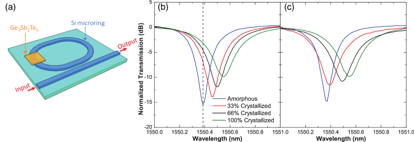
Reversible switching in PCM-tuned on-chip photonics devices was first demonstrated by Rude et al.[32] using a Si microring Resonator on-chip photonics device. Rather than exploiting the change in the imaginary part () of the refractive index, which is related to the optical absorption, this resonator device exploited the change in the real part of the refractive index (). The idea was to switch the optical path length of the resonator by increasing the Ren of a Ge2Sb2Te5 patch on the Si resonator waveguide, which in turn would change the the resonant wavelength of the device. Fig. 2(a) shows the schematic of the device. The resonant wavelength of the prototype devices could be reversibly switched from 1550.38 nm to 1550.55 nm. Moreover, changing the fraction of crystallised Ge2Sb2Te5 allowed the resonance to be tuned to any wavelength between 1550.38 nm to 1550.55 nm, see figure 2(b-c) The tuning was accomplished using an external 975 nm pump laser to heat the Ge2Sb2Te5 patch. The advantage of tuneable resonators is that they can be used to control the phase and amplitude of the wave emerging from the resonator; thus tuneable interference is possible. Indeed, this device also showed a 12 dB extinction ratio by exploiting the switch in Ren to destructively interfere the 1550.38 nn signal. A similar Ge2Sb2Te5 -tuned ring resonator that used a Si3N4 waveguide rather than Si was demonstrated in the same year by Rios et al[30]. Generally, absorption inside resonators decreases the amount of energy resonating, which concomitantly increases the width of the resonance. Since Ge2Sb2Te5 is relatively absorbing at 1550 nm, the ring resonators are relatively lossy and have broad resonances (Low Q-factor). Thus new low-loss PCMs are required to tune telecommunication wavelength ring resonators.
More recently, Rios et al. demonstrated that the transmitted intensity of 1550 nm light through a Si3N4 waveguide could be reversibly switched by heating the Ge2Sb2Te5 with a laser pump pulse[31]. Unlike the previous switching demonstrations, the pump pulse was also sent through the waveguide. The Ge2Sb2Te5 switches because a significant fraction of the guided mode is outside of the waveguide, and since the refractive index of Ge2Sb2Te5 is much larger than Si3N4 , the electric field of the propagating mode couples into the Ge2Sb2Te5. A stepwise partial recrystallization scheme was employed because amorphous Ge2Sb2Te5 has a much lower refractive index than the crystalline state; hence less energy is evanescently coupled to the amorphous Ge2Sb2Te5 patch, which makes single-shot crystallisation challenging.
Aside from switching the transmission of light in dielectric waveguides, surface plasmon polaritons (SPPs) and surface phonon polaritons (SPhPs) can also be switched using Ge2Sb2Te5 [33, 23]. The Drude model states that free electrons oscillate out of phase with the driving electric field, and therefore the dielectric permittivity of most metals is negative. Plasmons are collective oscillations of these free electrons at a well defined resonant frequency. SPPs are collective oscillations of free electrons at a metal-dielectric interfaces. In contrast, SPhPs can be excited by coupling light to polar crystals, which produces collective lattice vibrations at a well defined frequency. Both effects involve the interaction of electromagnetic radiation under the condition that , where the dielectric function is defined as . At visible frequencies SPPs tend to occur when light interacts with metallic nanostructures. Whilst mid-infrared frequencies are usually used to excite SPhPs. Both SPPs and SPhPs are highly confined guided modes, but SPhPs tend to have a much longer lifetime and are less lossy. Rude et al. showed that 1550 nm SPPs guided along a Au/SiO2 interface can be modulated by changing the structural state of a Ge2Sb2Te5 section, which is patterned on the SPP waveguide[33]. Conceivably, this type of device could be used to read the state of nanoscale electrical phase change random access memory devices using light, which would allow faster communication across a computer network. A schematic of the structure is shown in figure 3. Li et al. demonstrated that thin Ge2Sb2Te5 films on a polar crystal, such as quatz, can support M-IR SPhPs[23]. By laser crystallising two dimensional structures into the Ge2Sb2Te5 , high Q-factor mid-Infrared SPhP resonators were possible. Moreover, by switching the state of the Ge2Sb2Te5 the resonant wavelength could be tuned.
4 Planar thin film tuneable filters
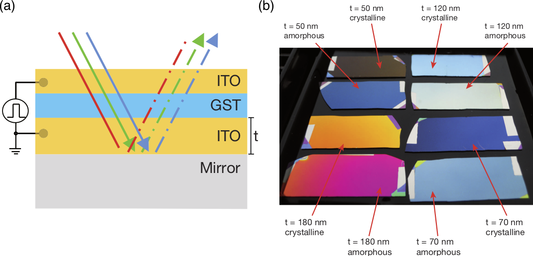
PCMs have been used to tune the reflectivity spectrum of planar filters. Hosseini showed that a simple structure consisting of ITO/Ge2Sb2Te5 /ITO layers can produce strong resonances in the visible spectrum[19]. The reflected colour is defined by the thicknesses of the ITO and Ge2Sb2Te5 layers. Essentially, this structure forms a thin film Fabry-Perot etalon. To ensure colour vibrancy, the Ge2Sb2Te5 films must be extremely thin so that energy is only absorbed when the wavelength of the incident light is resonant with the etalon. For example, in the Fig. 4 all of the colours are produced using just 7 nm thick Ge2Sb2Te5 films. The resonant wavelength is changed by controlling the thickness of the ITO layers, hence light is strongly absorbed by the Ge2Sb2Te5 at the resonant wavelength– in effect, at resonance the light passes through the Ge2Sb2Te5 film a large number of times, and therefore is strongly absorbed. However, at other wavelengths, which are off-resonance, the light is not strongly absorbed.
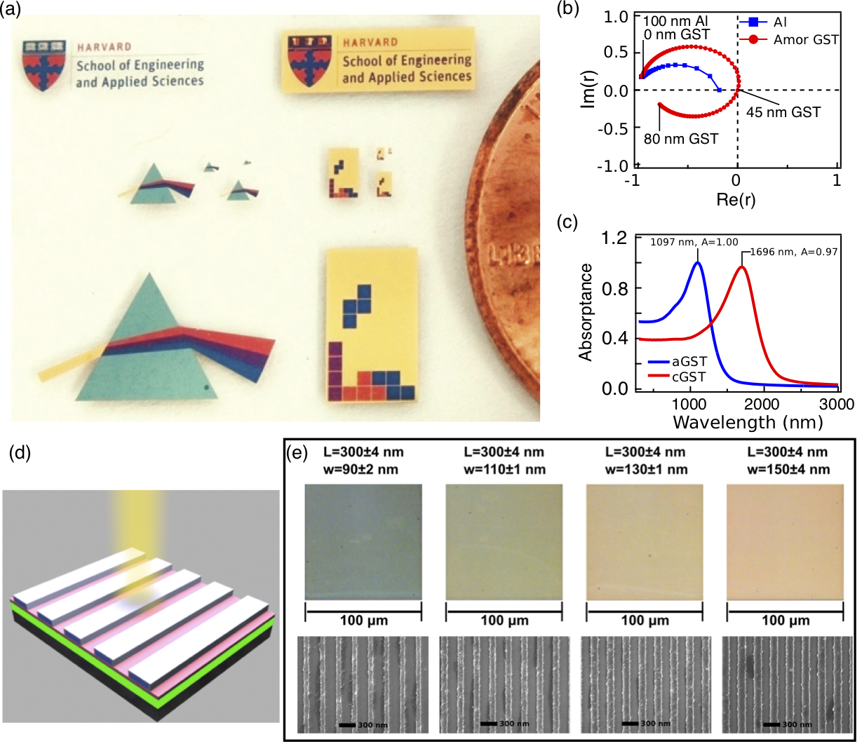
It is also possible to produce strong resonances by exploiting non- rad phase shifts using extremely thin absorbing films on reflective substrates. Figure 5(a) shows an example of this effect for 7, 11, 15, or 25 nm thick Ge films on a gold [21]. Complete destructive interference in these structures is possible by balancing the film’s absorption, with the the amplitude and phase of the the light reflected from each interface. Replacing the Ge layer with Ge2Sb2Te5 allows the peak absorption wavelength to be tuned over a wide range in the near infrared (N-IR). However, it is not possible to produce these resonances in the visible spectrum using planar structures. This is because the Ge2Sb2Te5 absorption coefficient in both crystalline and amorphous films is too large, and therefore the amplitude of light after passesing through the thin film structure is insufficient to cancel the light reflected from the Air-Ge2Sb2Te5 interface. However, at longer wavelength, such as 1097 nm and 1696 nm for the amorphous and crystalline state respectively, the Ge2Sb2Te5 absorption coefficient is lower, and the light reflected from buried interfaces is able to cancel the light reflected from the first air-Ge2Sb2Te5 interface. This is clearly seen in Fig. 5(b-c). Fig. 5(b) shows the complex reflection coefficient as a function of the Al-Ge2Sb2Te5 structure thickness. As the Al thickness is increased to 100 nm, the amount of light reflected increases. Since Al does not strongly transmit light, the path tracks relatively close to the real axis. At 100 nm Al, the Ge2Sb2Te5 layer is added, which causes the path to change track and follow a clock-wise direction. The Ge2Sb2Te5 is able to transmit the 1097 nm light, and we start to see the formation of a circular path in the complex plane. If the film was perfectly absorbing, then as the film thickness is increased, the reflection coefficient would cyclically track a circular path at a constant radius in the complex plane. However, Ge2Sb2Te5 has a non-zero absorption coefficient at a wavelength of 1097 nm, hence the the reflection coefficient follows a spiral path. We see that when the Ge2Sb2Te5 film is 45 nm thick, the path passes through the origin of the complex plane, which means that no light is reflected back from the structure. Indeed, this is confirmed in the Al –Ge2Sb2Te5 (45 nm) structure’s absorption spectrum, see Fig. 5(c). At 1097 nm we see that no light is reflected from the structure. However, when the Ge2Sb2Te5 is crystallised, the absorption at 1097 nm radically drops from 100% to aproximately 40%. This is because the crystalline Ge2Sb2Te5 film is now more absorbing and the radius of the reflection coefficient path is now much smaller, hence for the 45 nm thick film, the path does not pass through the origin. However, at a wavelength of 1696 nm, crystalline Ge2Sb2Te5 is far less absorbing, and the amount of light absorbed and reflected from the interfaces can balance again to produce near perfect absorption.
It should now be clear from Fig 5(b) that perfect absorption in the visible spectrum is not possible using dual layer metal–Ge2Sb2Te5 planar structures. This is because the absorption of Ge2Sb2Te5 is far too high at visible wavelengths and consequently the reflectance coefficient circle has a radius that is too short to pass through the origin of the complex plane. This conclusion can also be drawn by examining published reflectance spectra for related structures[36, 1]. However, other resonating structures, such as plasmonic structures, can be used to enhance the absorption at visible frequencies[17, 8]. Fig. 5(d) shows one such structure that we implemented. Al plasmonic gratings were used to generate plasmon resonances in the visible spectrum. These resonances couple to the absorbing Ge2Sb2Te5 film and produce strong broadband absorption peaks. The reflected colour is easily adjusted by controlling the dimensions of the gratings, as seen in Fig. 5(e).
The aforementioned reflective structures are relatively insensitive to the angle of incidence of the incoming light and can produce large changes in resonant wavelength. This is a clear advantage over thicker dielectric stacks that exploit multi-pass light circulation in resonant optical cavities. The simple planar structure means that they can be manufactured on an industrial scale using well established thin film deposition techniques, such as sputtering. The main disadvantage is that the peak absorption wavelength is strongly dependent on the intrinsic absorption of the film. As was seen, the absorption of Ge2Sb2Te5 is too high to allow completely destructive interference in the visible spectrum. Clearly, new PCMs need to be developed with low intrinsic absorption at visible frequencies. This topic is discussed in section 5.
Metamaterials consist of different materials with sub-wavelength features that are patterned to strongly interact with light. The light ‘feels’ an effective medium that results from the properties of the individual nano materials and their geometric arrangement. If the metamaterial nanoelements have a resonant response, then the phase of the light emerging from the nanoelement can also be controlled. And this allows concepts, such as optical phase arrays to be realised[45]. To date, most PCM-tuned metamaterial devices employ nanoscale plasmonic elements. Since the plasmon resonance of these structures depends on the refractive index of the surrounding material, the metamaterials’ optical response can be tuned by changing the PCM refractive index. The earliest example of this concept was presented by the Zheludev group. They used the crystallisation of amorphous Gallium Lanthanum Sulphide[38] to control plasmonic split-ring resonators[35]. The same group also designed a series of Ge2Sb2Te5 -based reconfigurable flat metasurface devices that refract and diffract light. A train of femtosecond laser pulses was used to write, erase and over-write binary and greyscale patterns into the Ge2Sb2Te5 phase change film. These pronounced two-dimensional refractive index patterns mould the wavefront of light emerging from the film thus focusing or steering the probe laser beam. In the following section we will discuss our work on plasmonic metasurfaces, which employ a different strategy to create tuneable infrared filters.
4.1 Metal–Dielectric–Metal Metasurface
Metasurfaces are capable of manipulating the phase and amplitude of light without bulky optics. Hence, they are attractive for compact and highly integrated optical systems. The idea of a metasurface is that rather than being confined to the conventional homageneuos materials, multiple materials can be patterned with features orders of magnitude smaller than the wavelength of light. These nanoscale features are key to the utilisation of phase change materials in tuneable metasurfaces. Reversibly switchable Ge2Sb2Te5 -based structures must be quenched at approximately Ks-1 for amorphisation[34]. In optical data storage technologies the quenching problem is circumvented using very thin PCM films. Indeed, the thermal design of the optical data storage disc structure is extremely important. A typical disc stack is composed of a polycarbonate substrate/Al (100 nm)/()0.8)-(O2)0.2 (20 nm)/Ge2Sb2Te5 (20 nm)/()0.8)-(O2)0.2 (140 nm). The Ge2Sb2Te5 layer absorbs the 650 nm laser light and heats in tens of nanoseconds, whilst the other layers remain cool and can quench this thin Ge2Sb2Te5 layer, which has a small thermal load, into an amorphous state. Thicker Ge2Sb2Te5 films are very difficult to amorphise because the thermal load is larger. Therefore, reversibly switchable phase change optical structures must also employ thin PCM layers. For split-ring resonator metasurfaces, a design compromise needs to be reached. This is because reducing the PCM volume produces a smaller change in the metasurface optical response due to the reduced amount of PCM interacting with the plasmon’s electric field. However, in different metasurface designs, such as metal-dielectric-metal (MDM) metasurfaces, the electric field is radically enhanced using gap plasmons in very thin dielectric layers[46, 15]. Therefore, we designed a range of MDM-metasurfaces with GST dielectric layers[11, 18, 7, 8, 6, 10, 9, 4, 5]. In these designs the electric field is enhanced in a PCM layer that is just a few tens of nanometers thick, which means the PCM can be quenched at the rates necessary for amorphisation by using the substrate as a heatsink. Moreover, the metasurface optical response is extremely sensitive to changes to the Ge2Sb2Te5 tuneable dielectric constant. Since GeTe-Sb2Te3 materials strongly absorb light at visible frequencies, we designed our structures to operate at photon energies below the band gap of the GeTe-Sb2Te3 alloys, i.e. in the mid-infrared where the absorption is very low[13].
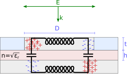
An electrical circuit model is useful for understanding the behaviour of plasmonic surfaces[49, 46, 44]. We can consider the principle parts of the MDM structure as inductor and capacitor elements. The electric field of the incident light forces the electrons to move, thus producing an electric current. This electric current produces a magnetic field; thus, the metallic elements behave an inductors. The electrons oscillate due to the driving oscillation of light’s electric field. When the electrons are at their extreme position in the metallic element, they are momentarily static, and there is no magnetic field. However, now the electrons create image charges in the bottom metallic layer of the MDM structure. This produces an enormous electrostatic field in the dielectric layer, and the charge separation can be modelled as a capacitor. Figure 6 shows a schematic of the MDM equivalent electrical circuit. Using this model, we can now describe the nature of the MDM optical response.
When we design tuneable MDM devices, our main aim is to use PCMs to control the structure’s resonant frequency. Using the circuit model shown in Fig. 6, we see that the structure can be modelled as an LRC circuit. The resonant frequency, , of an LC circuit is and therefore we should expect the resonant wavelength , to be . The inductance of a metal slab is correlated to its length and thickness, . Whilst the capacitance of the MDM structure depends on the dielectric’s thickness and permittivity, by . Therefore, we can now see how the MDM resonant wavelength depends on its geometry and materials, as shown by equation 1[44]: Here, is the metal layer thickness, is the dielectric thickness, is the dielectric refractive index, and is the length of the inductor.
| (1) |
From 1 we clearly see that the resonant wavelength red-shifts for increasing metal and dielectric film thicknesses and, importantly, when the dielectric’s refractive index increases. As one might expect, the resonant wavelength is also proportional to the size of the top metal features.
If the dielectric layer is replaced with a PCM, such as Ge2Sb2Te5, we see from equation 1 that the PCM’s large change in refractive index can be used to tune the the resonant wavelength of the structure. This resonant wavelength shift can be extremely large. In 2013 we designed a Au-Ge2Sb1Te4-Au MDM metamaterial perfect absorber that demonstrates this wide tuneablility[9]. The schematic of our design is shown in Figure 7(a-b). Essentially it consists of square array of 40 nm thick Au squares, which are pattern atop of a 40 nm thick continuous Ge2Sb1Te4 film, which in turn is on top of a 80 nm thick continuous Au film. The square lattice has a 1000 nm lattice constant, with Au squares with 900 nm long sides.
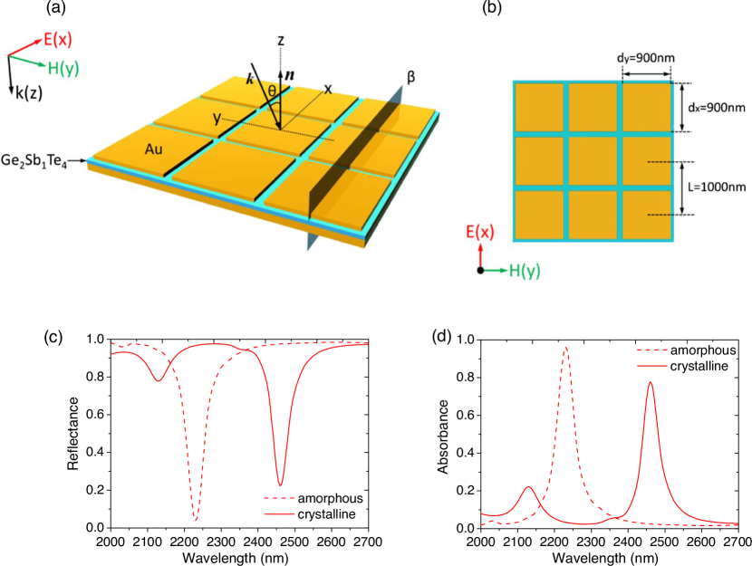
At resonance the absorption of the MDM Au square array metamaterial increases dramatically. This is because the effect of a small amount of absorption is amplified as the energy cycles back and forth. Thus, at resonance, troughs in the reflection spectrum are observed (see Fig. 7(c)), whilst peaks are seen in the absorption spectrum (see Fig. 7(d)). When the Ge2Sb1Te4 layer is in the amorphous state, the strongest resonance is at nm. However, if the Ge2Sb1Te4 layer is crystallised, the resonance shifts to nm due to the increased refractive index. This switching behaviour is predicted by equation 1.
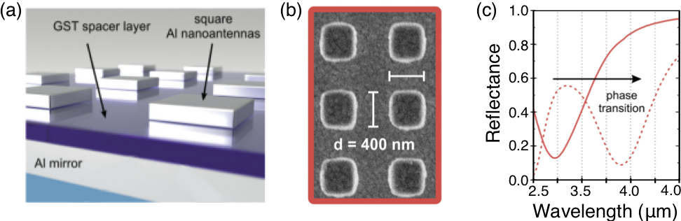
This type of MDM mid-infrared tuneable perfect absorber was successfully verified in 2015[40]. An array of square aluminium (Al) resonators stacked above a Ge3Sb2Te6 spacer layer and a bottom Al mirror was used to almost perfectly absorb mid-infrared light. Impressively, the absorption resonances could be red-shifted by 700 nm from 2700 nm to 3400 nm by crystallising the Ge3Sb2Te6 at 180° C. This is shown in fig. 8
For GeTe-Sb2Te3 –based photonic resonators the Q-factor of the resonance decreases when the PCM crystallises. This is because when GeTe-Sb2Te3PCMs crystallise, their electrical conductivity radically increases. Considering the LC circuit model (Fig. 6) once again, we see that if the PCM becomes conductive, a ‘shunt’ resistor forms in parallel with the capacitors. This, in turn, means that charge can easily leak away from the capacitors through their PCM spacer. Thus energy is lost from the resonator, and the Q-factor of the resonator drops. Indeed, slightly broader resonances are seen for the crystalline state in the measured absorption spectra presented by Tittl et al[40].
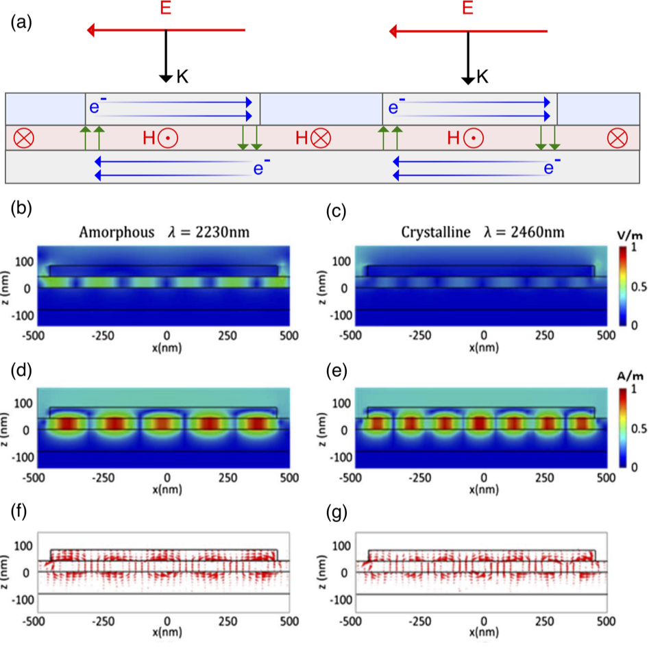
In order for these MDM structures to perfectly absorb light, both the electric and magnetic components of the incoming light must be efficiently absorbed. The incoming electric field forces free-electrons to move in the conductors, which are patterned on the surface of the MDM. As the electrons move, they induce image charges in the bottom conducting layer of the MDM structure, which move in the opposite direction. Fig. 9(a) shows a schematic of the MDM structure with electric field (), magnetic (-) field, and charge movements indicated. In the figure, charges moving in the metal layers are indicated by blue arrows, whilst displacement currents are highlighted by green arrows. The charge at the edge of the conducting squares is constantly changing with respect to time due to the cyclical nature of the incoming E-field. Thus a displacement current is generated through the dielectric spacer layer, and a current loop consisting of metallic and displacement currents is formed. These current loops generate a magnetic dipole, and consequently a magnetic dipole moment is also generated due to the incident H-field. Therefore, the H-field also strongly interacts with the structure, and is absorbed at resonance. If the structure is designed such that the H– and E– fields are resonant at the same frequency, then the incident light is perfectly absorbed. Figure 9(b-g) shows this effect for the phase change MDM structure presented in Fig.7. At resonance the and fields are tightly confined in the Ge2Sb1Te4 spacer layer. This is easily seen in the E-field (Fig. 9(b-c)) and H-field intensity (Fig. 9(d-e)) maps. The corresponding current loops are shown in Fig. 9(f-g). Strong magnetic moment generating current loops are present at resonance, which causes the observed strong peaks in Fig. 7
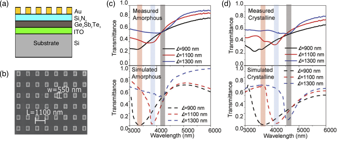
Most MDM metasurfaces are designed to reflect light, rather than transmit it. However transmission-type filters are attractive because they can be placed directly in front of detectors to create spectroscopy systems. These in-line designs are simpler than the reflective types, and consequently they can be used in highly compact integrated systems– such as in front of a camera CCD. However, the MDM structure usually consists of a bottom metallic reflector, which is required to create plasmon-image charges. Hence, if conventional materials are used, these devices cannot be transmissive. To solve this design-conflict we used Indium Tin Oxide (ITO), which is a transparent conductor, as the bottom electrode. The absorbtion of ITO can be tuned to become somewhat transparent in the M-IR by changing the oxygen content[22]. As is seen in Fig. 10, the transmission spectra shows resonances in the IR, which can be tuned by changing the phase of the Ge2Sb2Te5. Note, the resonances are broad because these structures are lossy due to the relatively high transparency of the bottom ITO layer.
We believe MDM metasurfaces have a high potential for real practical application because the PCM layer can be very thin, which is necessary for reversible switching, and only a single lithographic step is required to pattern the devices. Although electron beam patterning is impractical for large area industrial scale manufacturing, other Ge2Sb2Te5-tuned MDM structures that employ self-assembled plasmonic nanoparticles also show tuneable near perfect absorption[3], and we believe these can provide a low cost and high throughput route to commercialisation.
5 Material Development
The objective of this section is to introduce new materials that are being developed specifically for tuneable phase change photonics applications. New chalcogenide PCMs and alternative plasmonic materials will be discussed. In particular we will introduce Sb2S3 as a PCM for tuneable visible photonics, and discuss issues associated with diffusion and chemical reactions between chalcogenide PCMs and plasmonic metals.
PCMs, such as Ag-In-Sb-Te and those along the GeTe–Sb2Te3 pseudo-binary tie-line, are commercially proven technologies in re-writeable compact discs, digital versatile discs, and blu-ray discs. This is due to their large refractive index contrast between structural states[43], fast switching speed[41], scalability[37], availability, and proven commercial success in data storage applications. Clearly, it is attractive to start phase change photonics research with a technologically proven PCM, such as Ge2Sb2Te5. However, Ge2Sb2Te5 has a band gap of 0.5 eV in the crystalline state and 0.7 eV in the amorphous state[26]. This means that it is highly absorbing in the visible and in the near infrared part of the electromagnetic spectrum. Ge2Sb2Te5 only becomes transparent for wavelengths beyond where it retains a substantial change in the real component of the refractive index. This is most clear in Fig. 1, which shows the measured refractive index of Ge2Sb2Te5 to a wavelength of 3 m and the extrapolated refractive out to a wavelength of 6 m. The refractive index measurement and analysis details are given in reference [13], whilst the measurement data is open and available on www.actalab.com.
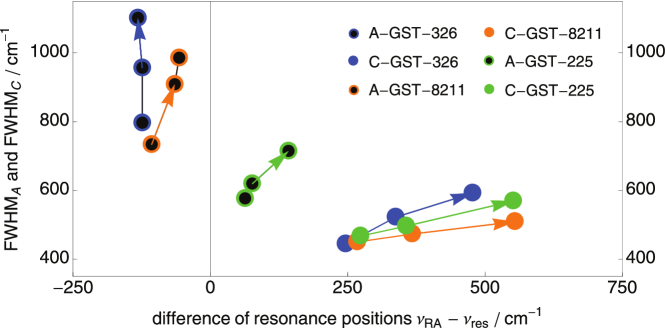
Despite the popularity of Ge2Sb2Te5 for tuneable M-IR photonics, there may be other Sb2Te3–GeTe compositions that are better suited to a particular application. Indeed, the Taubner group analysed the infrared optical properties of the Sb2Te3–GeTe pseudo-binary alloys with the aim of designing noble metal plasmonic resonators that exhibit sharp resonances in the infrared[27]. The Q-factor of any resonator is inversely proportional to the energy lost by the resonator during one cycle. It is, therefore, important to identify Sb2Te3–GeTe compositions with a low-loss in the IR. Fig. 11 shows the resonance Full Width Half Maximum (FWHM) for different antennae lengths (, , and nm), different Sb2Te3 –GeTe compositions, and different structural states of the PCM. These FWHMs measurements are plot against the difference between the antennae resonant frequency with, and without the PCM. As can be seen, Ge2Sb2Te5 exhibits the smallest shift in resonance frequency (). In comparison, the Ge3Sb2T6 and Ge8Sb2Te11 compositions offer a much broader tuning range; almost twice that of Ge2Sb2Te5. Ge3Sb2T6 has the largest resonant bonding character of the alloys studied, and therefore it is not surprising that antennae tuned by it show a large spectral change[27]. Optical losses in these structures are seen as a widening of the FWHM. In almost all the measurements, the Ge3Sb2T6 composition has the highest loss, whilst Ge8Sb2Te11 has the lowest loss. This is because Ge8Sb2Te11 has the largest band gap of the three materials, which sets the short wavelength absorption edge[27]. Its small carrier concentration also lowers the losses at IR frequencies associated with the Drude response[27]. The combination of lower losses and large tuning range means that the Ge8Sb2Te11 alloy has the largest tuning figure of merit, which is defined as, . is the change in the resonator’s frequency between amorphous and crystalline states, and FWHM is the full width half maximum of the resonance peak. Therefore, of all the PCMs along the Sb2Te3 -GeTe pseudobinary tie-line, Ge8Sb2Te11 offers the best compromise between Q-factor and tuning range. It is, therefore, recommended for tuning M-IR devices.
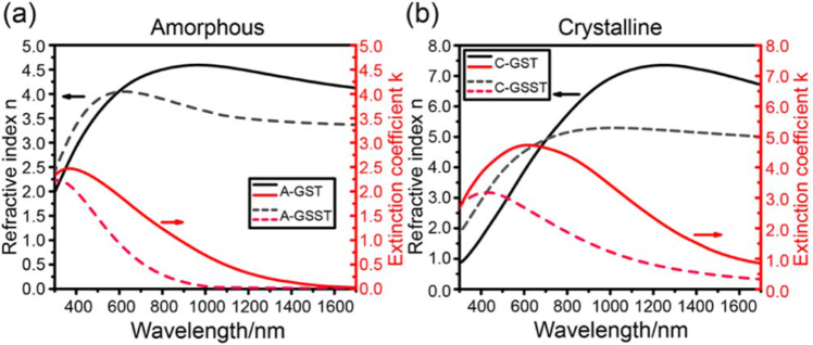
Optical losses for Sb2Te3–GeTe compositions in the N-IR and visible are extremely high, and therefore new PCMs must be developed for these frequency bands. The Hue group has developed the Ge2Sb2Se4Te1 by taking the Ge2Sb2Te5 alloy composition and substituting 80% of the Te with Se[48]. The optical constants for this material are compared with Ge2Sb2Te5 in figure 12. As can be seen, even after substituting the Te with Se, there is still a large change in Re(n), whilst the extinction coefficient, Im(n), is substantially lower in both crystalline and amorphous states. Although the optical band gap of the material is not given, we see that the amorphous state transmits wavelengths longer than 1 m. The crystalline state seems to have a long Urbach tail but is significantly less lossy than Ge2Sb2Te5 in the telecoms band. Early preprint results also suggest that this material can reversibly switch on a microsecond timescale and be cycled more than 1000 times between the crystalline and amorphous states[47].
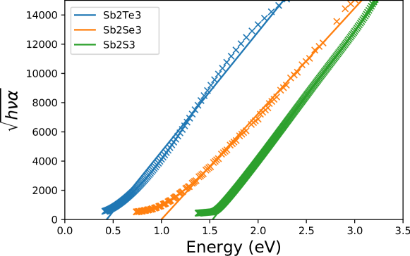
It is not surprising that substituting Te with Se in Ge2Sb2Te5 increased its optical band gap. As a rule of thumb, as lighter chalcogen atoms are replaced by heavier chalcogen atoms, moving down the periodic table from S to Se to Te, the band gap of the chalcogenide becomes smaller. Eventually the material becomes a metal or semi-metal. This is clearly seen for the Sb2M3 system, where M is either S, Se, or Te. We see from the Tauc plot, which is shown in Fig. 13, that the optical band gaps for Sb2S3, Sb2Se3, and Sb2Te3 are 1.5 eV, 1.0 eV, and 0.43 eV respectively[12, 16]. Since each of these materials stably exhibit optical contrast between their amorphous and crystalline states, these materials can be used as the basis to develop new PCMs for specific spectral regions.
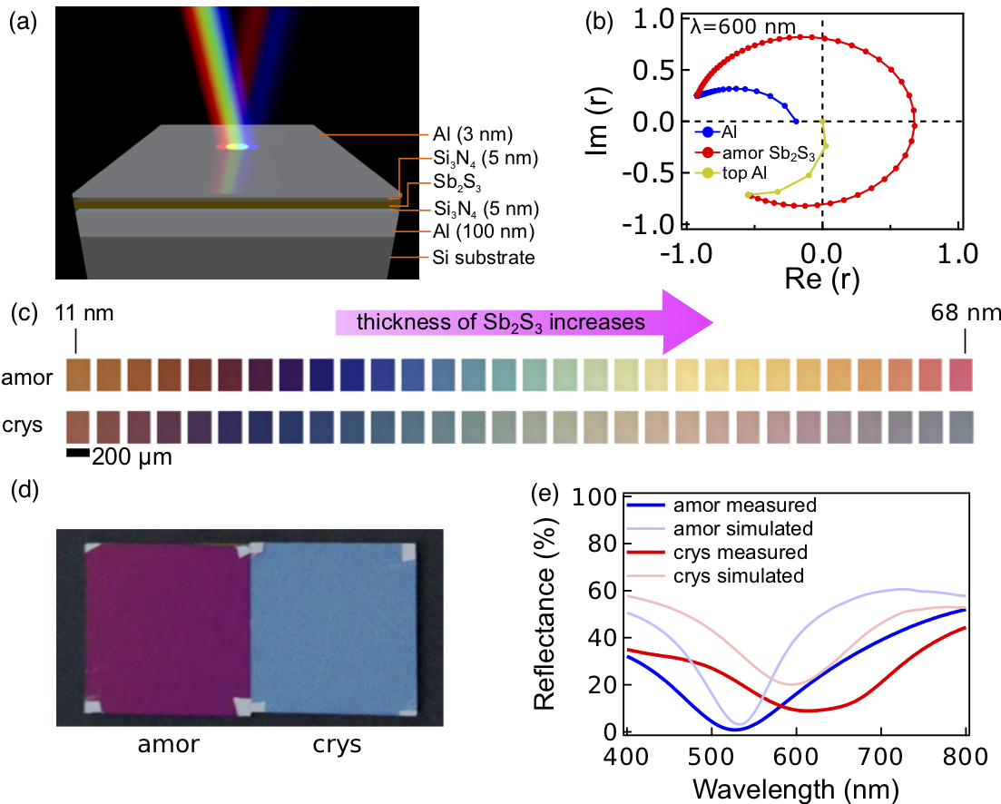
We aimed to use phase transition induced changes to the absorption coefficient to radically tune the colour of metal-Sb2S3 filters in the visible spectrum. We chose Sb2S3 because of its large band gap and concomitant lower absorption coefficient in the visible spectrum. We also found that this material is capable of reversible switching. It crystallises from the as-deposited amorphous state in just 70 ns[16]. This means that material can be used for high speed reprogrammable photonics applications. In section 4 we saw that when extremely thin absorbing semiconductor films are deposited on reflective metal films, perfect light absorption is possible via strong interference effects. However, the perfect absorption wavelength depends on the absorption coefficient of the film, and the intrinsic optical absorption of Ge2Sb2Te5 in the visible spectrum is too large to allow perfectly destructive interference. However, Sb2S3 has a much lower absorption coefficient at visible frequencies. Moreover, the absorption edge shifts from 2.05 to 1.70 eV when the material crystallises[16]. We designed, therefore, a metal–Sb2S3 thin film stack structure with a resonant frequency that couples at photon energies in the 2.05 to 1.70 eV range. Fig. 14(a) shows a schematic of the structure. We also included Si3N4 barriers to prevent any reactions between Sb2S3 and the Aluminium reflector layers. A 4 nm thick Aluminium top layer was also used to enhance the destructive interference. Indeed, as can be seen in Fig. 14(b), the top Aluminium layer causes the reflectance coefficient to pass through the origin of the complex plane circle diagram; thus allowing perfect destructive interference. Without this layer, the reflectivity at resonance will be much higher. Fig. 14(c) shows that changing the thickness of the Sb2S3 layer can produce a wide variety of vibrant colours. The Sb2S3 phase transition produces the largest spectral shift when the film is 24 nm thick. The colour changes from pink in the as-deposited amorphous phase to blue in the crystalline phase for the 24 nm thick Sb2S3 film. Photos of the film are included in Fig. 14(d), whilst the corresponding reflectance spectra are shown in Fig. 14(e). Note, that the vibrancy of the colours produced by combing metal and Sb2S3 films is due to low losses in the visible spectrum. When losses are high, the resonances are broader, which spreads the reflected wavelength across many colours thus causing a ‘greying’ effect.
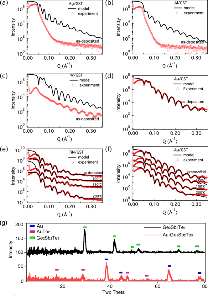
Aside from PCMs, it is also important to consider the materials that interface with the PCM. We have found that many plasmonic metals react or diffuse into Ge2Sb2Te5[25]. This is clearly seen in Fig. 15(a-f), which shows the measured X-Ray Reflectivity (XRR) plots of Ge2Sb2Te5 interface with different metals after annealing at different temperatures. The figure also includes the modelled XRR plots assuming that the interfaces are perfectly sharp. Silver, Aluminium, and Tungsten all seem to react with, or diffuse into, Ge2Sb2Te5 during the sample growth. From the XRR study, gold appears to be stable up to 200 ∘C but the X-Ray diffraction measurements (see 15(g)) clearly show the formation of AuTe2. We found that this reaction destroys resonances in thin film Au-Ge2Sb2Te5 filters[25]. To prevent these reactions, a diffusion barrier, such as a 5 nm thick Si3N4 film between the Ge2Sb2Te5 and gold, can be used. However, adding barriers between the PCM and plasmonic films is undesirable because it decreases the optical change induced by the PCM’s phase transition. Indeed, the PCM should be placed in direct contact with the plasmonic metal to maximise its overlap with the tightly confined surface plasmon electric field. Thus, we recommend TiN as the plasmonic material for PCM tuned plasmonic applications. We see that the TiN–Ge2Sb2Te5 XRR pattern shown in Fig. 15(e) almost exactly fits an XRR model of TiN/Ge2Sb2Te5 with sharp and smooth interfaces. This suggests that the measured layers have neither reacted nor inter-diffused. Importantly, the TiN visible dielectric function is very similar to that of gold[28], and TiN is a proven electrode heater material in Phase Change Random Access Memory devices[2]. The fact that the Ge2Sb2Te5 in PCRAM devices can be heated above the Ge2Sb2Te5 melting temperature millions of times when the devices are switched suggests that that TiN-Ge2Sb2Te5 interfaces are extremely stable.
6 Summary and Outlook
A variety PCM-tuned filters, metasurfaces, and On-Chip devices have been designed and prototyped. Often these devices exploit the well-known data storage PCMs along the Sb2Te3 -GeTe pseuduo-binary tie-line. We believe these particular compositions are most useful for tuning M-IR devices, where optical losses are low. Most of the current M-IR research focusses on the Ge2Sb2Te5 composition, however, detailed experimental studies have shown that Ge8Sb2Te11 exhibits the best compromise between optical losses and tuning range[27].
Since these PCMs require high quench rates to switch into the amorphous states, most of the prototype device demonstration only show one-way switching from the amorphous state to the crystalline state. A significant challenge is designing PCM-based photonic devices that can be reliably cycle between their amorphous and crystalline states. MDM structures use very thin PCM films to produce enormous changes to their optical response, whilst the PCM’s small thermal load also permits short quench times. For this reason, and because of their relatively simple design, we believe that MDM structures show the greatest promise for commercial application.
Aside from Sb2Te3 -GeTe PCMs, a number of new PCM compositions are being developed specifically for photonics applications. These materials tend to replace Te with S or Se. In particular we have focussed on Sb2S3, whilst others are exploring Ge2Sb2Se4Te1. Both materials have a significantly larger optical band gap than the Sb2Te3 -GeTe alloys, and they can be reversibly switched using sub-microsecond Joule heat pulses[16, 47].
When designing PCM-tuned photonic devices, it is also important to consider chemical reactions and inter-diffusion with the interfacing materials. For example, we have found that many plasmonic materials diffuse into or react with Ge2Sb2Te5[25]. Thus when designing tuneable plasmonic devices in the visible spectrum, we recommend using TiN for the plasmonic material. It can be interfaced directly with the PCM without reactions of inter-diffusion, and it can be used as the heating electrode for switching the material. If, other plasmonic materials must be used, then a thin barrier of an inert material should be included between the plasmonic metal and the PCM.
In conclusion, many PCMs exhibit tuneable electrical and optical properties, which have been exploited in electrical and optical memory technologies. However, we believe the next generation of PCM-based devices will exploit the electrical and optical properties simultaneously. There will be a growing need for these types of materials as their application is not limited to a single specific task; i.e. they are reconfigurable and may perform variety of photonic and electrical tasks. Thus, PCMs have the necessary plasticity to fuel smart multifunctional devices, systems, and networks. These types of devices will be an important-enabler of the Internet of Everything
Acknowledgements. We thank Professor Joel K. Yang for enjoyable and fruitful discussions. We are grateful for the hard work of our PhD students: Weiling Dong, Li Lu, Mr Libang Mao, and Kuan Liu. A substantial portion of the results presented in this chapter are the outcome of A-Star (A18A7b0028, 1420200046) and the Samsung Global Research Opportunity grants.
References
- [1] G. Bakan, S. Ayas, T. Saidzoda, K. Celebi, and A. Dana. Ultrathin phase-change coatings on metals for electrothermally tunable colors. App. Phys. Lett., 109(7):071109, 2016.
- [2] G. W. Burr, M. J. Breitwisch, M. Franceschini, D. Garetto, K. Gopalakrishnan, B. Jackson, B. Kurdi, C. Lam, L. A. Lastras, A. Padilla, B. Rajendran, S. Raoux, and R. S. Shenoy. Phase change memory technology. J. Vac. Sci. Technol. B, 28(2):223–262, 2010.
- [3] T. Cao, K. Liu, L. Lu, H.-C. Chui, and R. E. Simpson. Large-area broadband near-perfect absorption from a thin chalcogenide film coupled to gold nanoparticles. ACS Applied Materials & Interfaces, 2019.
- [4] T. Cao, R. E. Simpson, and M. J. Cryan. Study of tunable negative index metamaterials based on phase-change materials. J. Opt. Soc. Am. B, 30(2):439–444, Feb 2013.
- [5] T. Cao, C. Wei, R. E. Simpson, L. Zhang, and M. J. Cryan. Rapid phase transition of a phase-change metamaterial perfect absorber. Opt. Mater. Express, 3(8):1101–1110, 2013.
- [6] T. Cao, C. Wei, R. E. Simpson, L. Zhang, and M. J. Cryan. Fast tuning of double fano resonance using a phase-change metamaterial under low power intensity. Sci. Rep., 4, 2014.
- [7] T. Cao, C. Wei, R. E. Simpson, L. Zhang, and M. J. Cryan. Fast tuning of fano resonance in metal/phase-change materials/metal metamaterials. Optical Materials Express, 4(9):1775–1786, 2014.
- [8] T. Cao, C.-w. Wei, R. E. Simpson, L. Zhang, and M. J. Cryan. Broadband polarization-independent perfect absorber using a phase-change metamaterial at visible frequencies. Sci. Rep., 4, 2014.
- [9] T. Cao, L. Zhang, R. E. Simpson, and M. J. Cryan. Mid-infrared tunable polarization-independent perfect absorber using a phase-change metamaterial. J. Opt. Soc. Am. B, 30(6):1580–1585, Jun 2013.
- [10] T. Cao, L. Zhang, R. E. Simpson, C. Wei, and M. J. Cryan. Strongly tunable circular dichroism in gammadion chiral phase-change metamaterials. Opt. Express, 21(23):27841–27851, Nov 2013.
- [11] T. Cao, X. Zhang, W. Dong, L. Lu, X. Zhou, X. Zhuang, J. Deng, X. Cheng, G. Li, and R. E. Simpson. Tuneable thermal emission using chalcogenide metasurface. Adv. Opt. Mat., page 1800169, 2018.
- [12] C. Chen, W. Li, Y. Zhou, C. Chen, M. Luo, X. Liu, K. Zeng, B. Yang, C. Zhang, J. Han, and J. Tang. Optical properties of amorphous and polycrystalline sb2se3 thin films prepared by thermal evaporation. Appl. Phys. Lett., 107(4):043905, 2015.
- [13] L. T. Chew, W. Dong, L. Liu, X. Zhou, J. Behera, H. Liu, K. V. Sreekanth, L. Mao, T. Cao, J. Yang, and R. E. Simpson. Chalcogenide active photonics. Proc.SPIE, 10345:10345 – 10345 – 9, 2017.
- [14] C. R. de Galarreta, I. Sinev, A. M. Alexeev, P. Trofimov, K. Ladutenko, S. G.-C. Carrillo, E. Gemo, A. Baldycheva, V. K. Nagareddy, J. Bertolotti, et al. All-dielectric silicon/phase-change optical metasurfaces with independent and reconfigurable control of resonant modes. arXiv preprint arXiv:1901.04955, 2019.
- [15] F. Ding, Y. Yang, R. A. Deshpande, and S. I. Bozhevolnyi. A review of gap-surface plasmon metasurfaces: fundamentals and applications. Nanophotonics, 7(6):1129–1156, 2018.
- [16] W. Dong, H. Liu, J. K. Behera, L. Lu, R. J. H. Ng, K. V. Sreekanth, X. Zhou, J. K. Yang, and R. E. Simpson. Wide band gap phase change material tuned visible photonics. Advanced Functional Materials, (1806181), 2018.
- [17] W. Dong, Y. Qiu, J. Yang, R. Simpson, and T. Cao. Wideband absorbers in the visible with ultrathin plasmonic-phase change material nanogratings. J. Phys. Chem. C, 120(23):12713–12722, 2016.
- [18] W. Dong, Y. Qiu, X. Zhou, A. Banas, K. Banas, M. B. H. Breese, T. Cao, and R. E. Simpson. Tunable mid-infrared phase-change metasurface. Adv. Opt. Mat., (1701346), 2018.
- [19] P. Hosseini, C. D. Wright, and H. Bhaskaran. An optoelectronic framework enabled by low-dimensional phase-change films. Nature, 511(7508):206–211, 07 2014.
- [20] Y. Ikuma, Y. Shoji, M. Kuwahara, X. Wang, K. Kintaka, H. Kawashima, D. Tanaka, and H. Tsuda. Small-sized optical gate switch using ge2sb2te5 phase-change material integrated with silicon waveguide. Electronics Lett., 46(5):368–369, 2010.
- [21] M. A. Kats, R. Blanchard, P. Genevet, and F. Capasso. Nanometre optical coatings based on strong interference effects in highly absorbing media. Nat Mater, 12(1):20–24, 01 2013.
- [22] S. Lee, J. Pincenti, A. Cocco, and D. Naylor. Electronic and optical properties of room temperature sputter deposited indium tin oxide. Journal of Vacuum Science & Technology A: Vacuum, Surfaces, and Films, 11(5):2742–2746, 1993.
- [23] P. Li, X. Yang, T. W. W. Maß, J. Hanss, M. Lewin, A.-K. U. Michel, M. Wuttig, and T. Taubner. Reversible optical switching of highly confined phonon–polaritons with an ultrathin phase-change material reversible optical switching of highly confined phonon–polaritons with an ultrathin phase-change material. Nature Mater., Advanced Online Publication(–):–, May 2016.
- [24] D. Loke, T. H. Lee, W. J. Wang, L. P. Shi, R. Zhao, Y. C. Yeo, T. C. Chong, and S. R. Elliott. Breaking the speed limits of phase-change memory. Science, 336:1566–1569, 2012.
- [25] L. Lu, W. Dong, J. K. Behera, L. T. Chew, and R. E. Simpson. Inter-diffusion of plasmonic metals and phase change materials. J. Mater. Sci., 54(4):2814–2823, 2018.
- [26] H.-K. Lyeo, D. G. Cahill, B.-S. Lee, J. R. Abelson, M.-H. Kwon, K.-B. Kim, S. G. Bishop, and B. ki Cheong. Thermal conductivity of phase-change material . Appl. Phys. Lett., 89(15):151904, 2006.
- [27] A.-K. U. Michel, M. Wuttig, and T. Taubner. Design parameters for phase-change materials for nanostructure resonance tuning. Adv. Opt. Mat., 5(18), 2017.
- [28] G. V. Naik, J. L. Schroeder, X. Ni, A. V. Kildishev, T. D. Sands, and A. Boltasseva. Titanium nitride as a plasmonic material for visible and near-infrared wavelengths. Opt. Mater. Express, 2(4):478–489, Apr 2012.
- [29] A. Pirovano, A. L. Lacaita, A. Benvenuti, F. Pellizzer, S. Hudgens, and R. Bez. Scaling analysis of phase-change memory technology. In Electron Devices Meeting. IEDM ’03 Technical Digest., pages 699–702. IEEE International, 2003.
- [30] C. Rios, P. Hosseini, C. D. Wright, H. Bhaskaran, and W. H. P. Pernice. On-Chip Photonic Memory Elements Employing Phase-Change Materials. Adv. Mater., pages 1521–4095, 2013.
- [31] C. Rios, M. Stegmaier, P. Hosseini, D. Wang, T. Scherer, C. D. Wright, H. Bhaskaran, and W. H. P. Pernice. Integrated all-photonic non-volatile multi-level memory. Nat Photon, 9(11):725–732, 11 2015.
- [32] M. Rudé, J. Pello, R. E. Simpson, J. Osmond, G. Roelkens, J. J. van der Tol, and V. Pruneri. Optical switching at 1.55 m in silicon racetrack resonators using phase change materials. App. Phys. Lett., 103(14):141119, 2013.
- [33] M. Rude, R. E. Simpson, R. Quidant, V. Pruneri, and J. Renger. Active control of surface plasmon waveguides with a phase change material. ACS Photonics, 2(6):669–674, 2015.
- [34] M. Salinga, E. Carria, A. Kaldenbach, M. Bornafft, J. Benke, J. Mayer, and M. Wuttig. Measurement of crystal growth velocity in a melt-quenched phase-change material. Nat Commun, 4, 08 2013.
- [35] Z. L. Sámson, K. F. MacDonald, F. De Angelis, B. Gholipour, K. Knight, C. C. Huang, E. Di Fabrizio, D. W. Hewak, and N. I. Zheludev. Metamaterial electro-optic switch of nanoscale thickness. App. Phys. Lett., 96(14):–, 2010.
- [36] F. F. Schlich, P. Zalden, A. M. Lindenberg, and R. Spolenak. Color switching with enhanced optical contrast in ultrathin phase-change materials and semiconductors induced by femtosecond laser pulses. ACS Photonics, 2(2):178–182, 2015.
- [37] R. E. Simpson, P. Fons, A. V. Kolobov, T. Fukaya, M. Krbal, T. Yagi, and J. Tominaga. Interfacial Phase-Change Memory. Nature Nanotech., 6:501 – 505, 2011.
- [38] R. E. Simpson, A. Mairaj, R. J. Curry, C.-C. Huang, K. Knight, N. Sessions, M. Hassan, and D. W. Hewak. Electrical phase change of Ga: La: S: Cu films. Electronics Letters, 43(15):830–832, 2007.
- [39] D. Strand, D. V. Tsu, R. Miller, M. Hennessey, and D. Jablonski. Optical routers based on ovonic phase change materials. In European Phase Change and Ovonics Symposium (E/PCOS), 2006.
- [40] A. Tittl, A.-K. U. Michel, M. Schäferling, X. Yin, B. Gholipour, L. Cui, M. Wuttig, T. Taubner, F. Neubrech, and H. Giessen. A switchable mid-infrared plasmonic perfect absorber with multispectral thermal imaging capability. Adv. Mater., 27(31):4597–4603, 2015.
- [41] L. Waldecker, T. A. Miller, M. Rude, R. Bertoni, J. Osmond, V. Pruneri, R. E. Simpson, R. Ernstorfer, and S. Wall. Time-domain separation of optical properties from structural transitions in resonantly bonded materials. Nat. Mater., 14(10):991–995, 07 2015.
- [42] N. Yamada, E. Ohno, N. Akahira, K. Nishiuchi, K. Nagata, and M. Takeo. High speed overwritable phase change optical disk material. Jpn. J. Appl. Phys, 26-4:61–66, 1987.
- [43] N. Yamada, E. Ohno, K. Nishiuchi, N. Akahira, and M. Takao. Rapid phase-transitions of pseudobinary amorphous thin-films for an optical disk memory. J. Appl. Phys., 69(5):2849–2856, 1991.
- [44] J. K. W. Yang and R. E. Simpson. Plasmonic color webinar, November 2018.
- [45] N. Yu and F. Capasso. Flat optics with designer metasurfaces. Nature Materials, 13:139 EP –, 01 2014.
- [46] S. Zhang, W. Fan, N. Panoiu, K. Malloy, R. Osgood, and S. Brueck. Experimental demonstration of near-infrared negative-index metamaterials. Phys. Rev. Lett., 95(13):137404, 2005.
- [47] Y. Zhang, J. B. Chou, J. Li, H. Li, Q. Du, A. Yadav, S. Zhou, M. Y. Shalaginov, Z. Fang, H. Zhong, et al. Extreme broadband transparent optical phase change materials for high-performance nonvolatile photonics. arXiv preprint arXiv:1811.00526, 2018.
- [48] Y. Zhang, J. Li, J. Chou, Z. Fang, A. Yadav, H. Lin, Q. Du, J. Michon, Z. Han, Y. Huang, H. Zheng, T. Gu, V. Liberman, K. Richardson, and J. Hu. Broadband transparent optical phase change materials. Opt. Lett., 43(1):94–97, 2017.
- [49] D. Zhu, M. Bosman, and J. K. W. Yang. A circuit model for plasmonic resonators. Opt. Express, 22(8):9809–9819, Apr 2014.