A Graph-Theoretic Approach for Spatial Filtering and Its Impact on Mixed-type Spatial Pattern Recognition in Wafer Bin Maps
Abstract
Statistical quality control in semiconductor manufacturing hinges on effective diagnostics of wafer bin maps, wherein a key challenge is to detect how defective chips tend to spatially cluster on a wafer—a problem known as spatial pattern recognition. Recently, there has been a growing interest in mixed-type spatial pattern recognition—when multiple defect patterns, of different shapes, co-exist on the same wafer. Mixed-type spatial pattern recognition entails two central tasks: (1) spatial filtering, to distinguish systematic patterns from random noises; and (2) spatial clustering, to group filtered patterns into distinct defect types. Observing that spatial filtering is instrumental to high-quality mixed-type pattern recognition, we propose to use a graph-theoretic method, called adjacency-clustering, which leverages spatial dependence among adjacent defective chips to effectively filter the raw wafer maps. Tested on real-world data and compared against a state-of-the-art approach, our proposed method achieves at least % gain in terms of internal cluster validation quality (i.e., validation without external class labels), and about % gain in terms of Normalized Mutual Information—an external cluster validation metric based on external class labels. Interestingly, the margin of improvement appears to be a function of the pattern complexity, with larger gains achieved for more complex-shaped patterns.
Index Terms:
Clustering, Graph theory, Pattern recognition, Spatial data science, Unsupervised learning, Wafer bin maps.I Introduction
Integrated circuits (IC), colloquially known as chips, are essential to most, if not all, electronic devices. The central step in IC manufacturing is wafer fabrication, in which a batch of chips are fabricated on round-shaped silicon wafers through a series of complex electrochemical processes including slicing silicon-rich ingots into round-shaped thin wafers, wafer oxidation and material deposition, photolithography, ion implantation, and etching [1]. Once fabricated, all wafers undergo an operational quality performance test, known as wafer probing, in which chips are labeled as functional or defective by passing an input signal and collecting the corresponding output. This step results in a two-dimensional graphical representation called a wafer bin map—a gridded representation of a wafer in which each grid point represents the spatial location of a chip and is assigned a binary value (e.g., or ) denoting a functional or a defective chip, respectively. Figure 1 shows examples of three different wafer bin maps resulting from wafer probing tests, where defective chips are denoted by red squares.
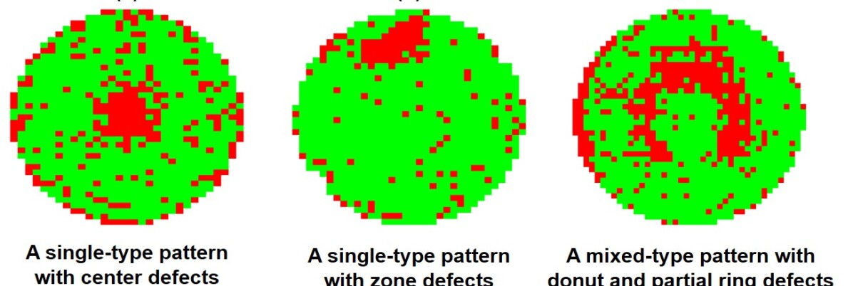
A careful analysis of wafer bin maps is pivotal to quality control efforts in the semiconductor manufacturing industry. By investigating the spatial defect patterns on the fabricated wafers, i.e., how the defective chips tend to spatially cluster, one can infer instrumental insights about the root causes of defect occurrence, and subsequently suggest corrective actions to mitigate future failures. This problem, often referred to in the literature as spatial pattern recognition (SPR), is the focus of this paper. SPR is of extreme importance to pinpoint possible root causes of failures in wafer fabrication. In fact, several spatial defect patterns in wafer bin maps can be directly traced to common root causes of failure. For instance, a circular-shaped, center-located defect pattern, as shown in Figure 1(a), often corresponds to chemical stains or mechanical equipment faults [2, 3], while a zone-shaped, edge-located defect pattern, as shown in Figure 1(b), can be traced to uneven polishing or edge-die effects [4]. A center-located, donut-shaped defect pattern, as shown in Figure 1(c), is routinely observed in wafer data due to possible tooling problems [5]. These spatial patterns like center, zone, or donut, wherein defective chips “cluster” to form distinct shapes are referred to as systematic patterns since they correspond to an assignable root cause. In contrast, randomly scattered defective chips in Figure 1(a)-(c) are called random patterns, or noises, since they are merely artifacts of random process variation.
In the SPR literature, defect patterns in wafer bin maps can either be single-type or mixed-type. The former refers to wafer maps that host only one defect pattern, while the latter refers to wafer maps in which two or more defect patterns co-exist. Figure 1(a-b) show examples of single-type defect patterns, whereas Figure 1(c) depicts a mixed-type defect pattern. With the ever-growing increase in scale and sophistication of the wafer fabrication process, mixed-type patterns are increasingly observed in production data. Barring few recent efforts [3, 6, 7, 8, 9, 10], the problem of mixed-type SPR has received less attention relative to its single-type counterpart.
A typical SPR analysis of a wafer bin map, be it hosting single- or mixed-type patterns, involves two pillar tasks: (1) Spatial filtering, i.e., to de-noise raw wafer data by separating systematic from random patterns; and (2) Spatial clustering, i.e., to group the filtered patterns into one or more sub-clusters pertaining to different types of defect patterns (e.g., center, donut). The overwhelming majority of the literature has been devoted to improving the effectiveness of the second task, namely spatial clustering, among which those that are based on model- or density-based clustering [11, 12, 2, 13, 14], kernel-based clustering [15, 16], similarity-based metrics such as correlograms, nearest-neighbor measures, or Voronoi-based partitioning [17, 18, 19], feature extraction-based approaches such as those utilizing Hugh transforms, single value decomposition, or mask-based features [20, 21, 22, 23], decision trees and manifold learning [24, 25], regression-based consensus networks and ensemble learning [24, 26, 27], and neural networks, especially those based on adaptive resonance theory [28, 29, 30, 31, 32, 33], or on deep learning-based architectures [34, 35, 36, 37, 38, 39, 40, 41, 42].
On the other hand, methods for the first task, namely spatial filtering, are mostly dominated by ad hoc heuristics intended to pre-process or denoise the raw wafer data, with an implicit assumption that the deficiencies of a poorly designed filtering step will be ultimately corrected in the second task (spatial clustering). While this assumption may be acceptable for single-type SPR, we claim that spatial filtering is of extreme importance to mixed-type SPR. Motivated by a similar observation, an algorithm called connected path filtering (CPF) has been recently proposed to filter mixed-type wafer bin maps [3]. The authors proposed to pair CPF with a spatial clustering model that acts on the filtered data to produce the final SPR results. CPF is a heuristic algorithm that searches all possible connected paths of defective chips on a wafer and only keeps those paths that are longer than a pre-set threshold, .
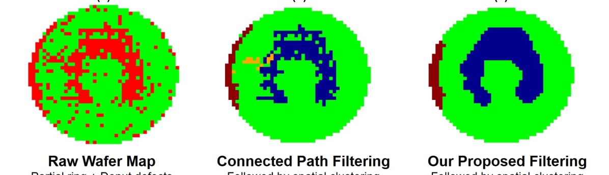
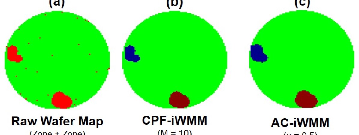
While valuable on its own, our analysis of multiple wafer maps, as we will elaborate in the sequel, has revealed two main limitations of the CPF approach. First, CPF does not directly leverage local spatial neighborhood information, but instead, it disregards all defective chips that do not belong to a connected path which is longer than a globally pre-set value, . In other words, if a chip is labeled as “functional,” while all of its neighbors are not, CPF does not make use of the local neighborhood information to possibly re-assign the label of this chip. A direct consequence of this limitation is that the filtered results may end up having irregular shapes (few functional chips surrounded by large groups of defective chips, or vice-versa), which may severely compromise the quality of the downstream clustering task. To demonstrate this first limitation, let us take a look at Figure 2, where Panel (a) shows a raw wafer bin map with a mixed-type pattern comprising partial ring and donut defects. The results from CPF (Panel b) clearly show an irregular shape due to either functional chips for which the values should have been updated to defective based on their local neighborhood, or alternatively, defective chips which should have been re-labeled as functional. This irregularity in the shapes misleads the downstream spatial clustering (performed using a mixture model—to be reviewed later) to mistakenly identify some defective chips as independent sub-clusters. The results in Panel (c) appear to be more visually appealing with a clear visual distinction between the two overlapping defect types, making the downstream clustering method (performed using the same mixture model) relatively straightforward. The result in Panel (c) is in fact, produced by our proposed filtering approach, for which the details are unraveled in Section II.
The second limitation of the CPF approach is its choice of . Our findings, to be presented in Section III, suggest that there does not appear to be a default value for that works universally well for all wafers and combinations of defect types, making the choice of wafer-specific. As outlined by the authors in [3], this choice is made via interaction with domain experts. This limitation may severely hamper the applicability of CPF in practice. Given the large production volumes typical of wafer production lines, the need for domain experts to constantly weigh in and update the value of can be extraordinarily inefficient and thus impractical.
Motivated by the need to address those two limitations, we propose an innovative approach for mixed-typed SPR in wafer bin maps. Our major finding is that a graph-theoretic approach which leverages the local spatial dependence structure can considerably improve the spatial filtering step, and ultimately, the overall SPR quality. Specifically, we propose to use the adjacency-clustering (AC) method, which was originally introduced by [43] for yield prediction. Although technically similar, the main function of AC in our work is different from that in [43]: we focus on extracting systematic defect patterns (i.e., diagnostic analysis), rather than yield prediction (i.e., prognostic analysis). This distinction drives a fundamental departure in what constitutes a cluster: In [43], they define a cluster as a group of chips with homogeneous yield level, while our approach defines a cluster based on its chips’ membership in either the set of systematic or random defect pattern clusters. AC is closely tied to Markov Random Field (MRF) models which have been successfully applied in image segmentation and restoration [44, 45], spatial clustering [46], and wafer thickness variation analysis [47].
We couple the proposed spatial filtering method with a mixture model for spatial clustering. Based on the numerical experiments with real-world data, we show that our approach outperforms the state-of-the-art method in [3] by at least % in terms of internal cluster validation quality (i.e. validation without external information about class labels), and about % in terms of Normalized Mutual Information—an external cluster validation metric which makes use of externally provided class labels. The mixture model used for spatial clustering is the same as that used by [3] so that the improvements in the final clustering quality are solely attributed to our proposed filtering method. Interestingly, the margin of improvement appears to be a function of the defect pattern complexity, with larger gains achieved for more complex-shaped patterns.
In summary, our main contribution is to propose a graph-theoretic spatial filtering method which effectively distinguishes the random noises that are prevalent in wafer bin maps from systematic patterns, which are often attributed to well-studied root causes. There is an overwhelming evidence in the distant and recent literature that a poorly designed filtering method can have substantial detrimental impacts on the SPR performance in wafer bin maps, even with the emergence of powerful deep learning-based approaches [36, 38, 40, 6]. Unlike existing filtering and pre-processing methods, our approach fully leverages the spatial dependence information (via its graph-theoretic structure), and is not vulnerable to arbitrary parameter selections (e.g. filter size or length thresholds) which can be wafer-specific, thus requiring continuous intervention of domain experts. Furthermore, our method is shown to have a desirable combinatorial structure which can be solved in polynomial time by a minimum-cut algorithm. When coupled with a spatial clustering approach (in this paper, a mixture model), substantial improvements in SPR performance are detected, owing to the abovementioned advantages. In principle, we could replace this mixture model by any clustering or classification approach, thus emphasizing the generality and substantial benefit brought about by our proposed spatial filtering method.
We conclude this Section by describing the organization of this paper. In Section II, we elucidate the building blocks of our proposed approach, which comprises the details of the AC approach to filter the wafer maps, coupled with an advanced mixture model to further group the AC-filtered results into one or more sub-clusters corresponding to different systematic defect patterns. Section III presents our case study which details the analysis of twelve real-world wafer bin maps exhibiting complex multi-type defect patterns. Section IV concludes this paper and highlights future research directions.
II Our Approach
We represent a wafer map with chips by , where is the number of defects on chip . The locations of chips can be modeled as a graph where nodes denote chips and the edges define the neighborhood relationship, i.e., we have an edge when chip and chip are adjacent to each other on the wafer map. According to the neighborhood system, each chip can have at most four neighbors (rook-move neighborhood) or eight neighbors (king-move neighborhood).
Our SPR framework consists of two stages: a spatial filtering stage, and a spatial clustering stage, both of which are clustering tasks, yet they serve different purposes. In the first stage, namely spatial filtering, AC partitions the wafer map into two clusters, such that one of them only includes those chips that form systematic defect patterns. As a result, we are able to separate the systematic patterns (those caused by assignable root causes) from the random patterns (artifacts of random process variation). In the second stage, the AC-filtered results are further partitioned into one or more sub-clusters using a mixture model called the infinite warped mixture model (iWMM). Each sub-cluster corresponds to a type of systematic defect pattern, e.g., a center or zone, as shown in Figure 1.
II-A Adjacency-Clustering for Spatial Filtering
We sketch here the AC model from [43] and present how it can be adapted into the mixed-type SPR problem. The AC model aims to partition the set of chips into clusters such that chips belonging to the same cluster behave similarly and tend to be adjacent to each other. This AC concept is motivated by the spatial dependence among adjacent chips, which aligns well with the concept of the systematic defect patterns on a wafer map where defective chips tend to spatially cluster. In the case of binary defect data (i.e., ), the AC model will find two clusters: the first cluster corresponds to the set of systematic defect patterns, while the other corresponds to random defect patterns.
The clustering decisions are cluster labels for . Chips with the same label form a single cluster. The objective function of AC includes a deviation cost function and a separation cost function. The deviation cost function measures how deviates from the observed value , while the separation cost function captures the difference in assigned labels of adjacent chips. Let denote the deviation cost functions associated with node and denote the separation cost functions for edge . AC can be formulated as the following integer program:
| (AC) | ||||
| (1) |
where is the set of allowable labels of each chip. In our application, we have .
The clustering results depend on the trade-off between the two cost functions. When the separation function values are relatively larger than the deviation function values, the resulting clusters will be more contiguous (the spatial smoothing effect is more significant). If the separation costs are too large, the whole wafer map would be forced to have the same label so the separation cost is minimized. On the other hand, when the separation costs are small, the assigned labels will be close to the original observational values and the spatial filtering effect is less notable in the clustering result. The AC model has a statistics foundation from Markov random fields (MRF) wherein solving for is finding the maximum a posterior (MAP) estimate of the degradation model with an MRF prior [45]. Different forms of separation and deviation functions reflect different distributional assumptions of MRF.
The neighborhood system also plays an important role in the AC results. When the rook-move neighborhood structure is assumed, the clustering only looks for defect patterns that grow horizontally or vertically. By contrast, with the king-move structure, the clustering will identify defect patterns that exhibit more complex shapes such as ring and donut patterns. Therefore, the king-move structure can work better for complicated clustering tasks, as those prevalent in mixed-type defect detection (See Figure 2(c) for an example).
When both and are binary (), as in our SPR application, then the AC model reduces to the problem called minimum s-excess [48]:
| (AC-BIN) | ||||
| (2) | ||||
| (3) | ||||
| (4) |
where indicates the difference in the label values of chip and , while is the deviation cost of chip , and is the separation cost associated with the pair of chips. More specifically, for chips with and for chips with : (1) when , we will incur a penalty of for labeling and zero penalty otherwise, so the associated deviation cost is and ; (2) when , we will incur a penalty of when assigning and zero penalty otherwise, hence the associated deviation cost is ; After dropping the constant, we get . And for all pairs (the separation cost is 0 if ). The reduction to the minimum s-excess is attainable for any deviation and separation functions.
The minimum s-excess problem can be solved in polynomial time with a minimum-cut algorithm applied to an appropriately defined graph [48]:
Proposition 1.
The adjacency-clustering model with binary label values (AC-BIN) can be solved in polynomial time.
Proof.
First, we can verify that the constraint matrix of (AC-BIN) is totally unimodular and therefore, (AC-BIN) can be solved in polynomial time. Second, the constraints also correspond to the dual of the minimum cost network flow problem. Then finding the solution to (AC-BIN) is equivalent to finding the minimum cut on a graph adapted from [48]. ∎
The algorithm constructs a graph as follows: First we add to a source node and a sink node , and each edge is replaced by two arcs and with the same capacity of . For each node with a positive , we add an arc of capacity from the node to the sink. For each node with a negative weight , we add an arc of capacity from the source. Then the defective cluster (the set of chips with ) is the source set of a minimum cut in . The computational results indicate that this algorithm can solve instances with thousands of chips within seconds, which facilitates its real-time adoption in practice.
If and take more than two values, the AC model can still be solved in polynomial time for convex deviation and separation functions. Specifically, for “bilinear” separation cost functions (i.e., if and otherwise) and any convex deviation function, [48] devised an algorithm that solves the problem in the running time of a single minimum cut (and the running time of finding the minima of the convex deviation functions). This time complexity was also shown by [48] to be the best that can be achieved. When the separation cost function is not “bilinear” but convex, the Lagrangian relaxation technique can be applied for the polynomial time algorithm [49] .
After solving AC with binary label values, each chip is assigned a new label. The chips with a label value of one form a cluster that contains systematic defect patterns, while the chips with a label value of zero are filtered out. In other words, the original defects recorded on the zero-label chips are treated as random defect patterns of nonassignable causes, to be marked off by the spatial filtering stage and thus no longer deemed defects in the subsequent spatial clustering stage. The spatial filtering result depends on the relative magnitude of the separation costs and deviation costs (the relative differences between and in AC-BIN). As we show in Section III, our numerical analysis suggests that there is a set of parameter values that yields consistently high quality SPR results.
II-B Infinite Warping Mixture Model for Spatial Clutering
Given the AC-filtered results, we apply iWMM [50] to group the resulting systematic patterns into sub-clusters pertaining to distinct types of defect patterns. Before we elaborate on the details of iWMM, we first briefly discuss the motivation of using it in our setting. iWMM was first proposed by [50] and then adopted by [3] to spatially cluster the wafer maps that are filtered via CPF. In our approach, we keep the iWMM as our spatial clustering method, because iWMM is a highly potent multi-class clustering method and lends itself well to the SPR problem (more about this in the following). Additionally, by using the same spatial clustering method as that used by [3], we ensure that the improvements in SPR quality are mainly attributed to our proposed filtering method.
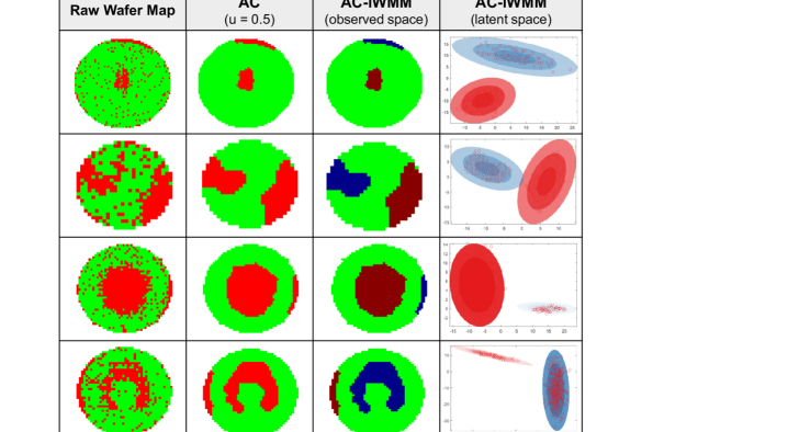
The benefit of using iWMM in spatial clustering of wafer defect patterns is two-fold. First, in iWMM, the number of sub-clusters corresponding to the number of defect types on a wafer is estimated rather than specified a priori—a common shortfall of most clustering methods. Second, and more importantly, defects in wafer maps tend to have non-Gaussian shaped patterns (such as donut and ring). This invalidates the assumptions of many classical model-based clustering approaches that assume the clusters themselves follow a certain parametric distribution (most commonly a Gaussian). The iWMM method relaxes this assumption by making the parametric distribution assumption on the clusters in a latent space, which are related to the original complex-shaped clusters through a non-linear transformation called a warping function. Through this warping, complex non-Gaussian-like shapes in the observed space can be represented by simple Gaussian-like shapes in the latent space. Clustering is then performed in the latent space using a model-based clustering technique (e.g. Gaussian mixture). Figure 3 shows an example of how iWMM works within our framework.
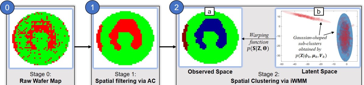
We briefly describe the key details of the iWMM method in our problem setting and interested readers can refer to the Appendix for more details. As evident in Figure 3, two building blocks constitute the essence of iWMM: (1) a warping function to match the observed spatial locations of the AC-filtered results with a set of latent spatial coordinates in the latent space, and (2) a model-based clustering method which determines the clustering assignments in the latent space. The authors in [50] propose to use a Gaussian process latent variable model (GPLVM) [51] as a warping function, and an infinite Gaussian mixture model (iGMM) as a model-based clustering method. We briefly review both in the sequel.
Using the notation from Section II, we denote by the set of spatial locations of the defective chips in the AC-filtered results, i.e. for which , where , and . The set in the observed space corresponds to a set of latent coordinates in the latent space denoted by , where . The ultimate goal of iWMM is to find a vector of assignments in the latent space, denoted as , where denotes the membership of the th chip to a particular sub-cluster.
GPLVM is used to map (or warp) the transformed spatial locations , which are assumed to follow a Gaussian distribution, into the observable space where can have a non-Gaussian distribution. For GPLVM, the conditional probability of given is expressed as in Eq. (5) [51].
| (5) |
where tr() is the trace function, is the determinant operation, and is an covariance matrix whose th and th entry holds the covariance between a pair of observations and . To determine the entries of , a stationary parametric covariance function is selected, which depends on the lag between a pair of inputs through a set of hyperparameters . A popular choice for is the so-called squared exponential covariance [52], which is employed in this work.
Once the warping function is established, iGMM is used for spatial clustering in the latent space by assuming that the th mixture component (or sub-cluster) in the latent space follows a Gaussian distribution with a mean and precision matrix, denoted by and , respectively. Each mixture component is associated with a mixture weight, . The mathematical expression for iGMM is presented in Eq. (6).
| (6) |
A detailed procedure to fit the iWMM to a set of observed spatial locations is proposed in [50], where the latent coordinates , assignments , as well as remaining parameters are inferred through a Markov Chain Monte Carlo (MCMC)-based procedure. The implementation codes for iWMM have been made publicly available [53] and we use them for our numerical analysis in Section III.
III Application to Real-World Wafer Map Data
In this section, we evaluate the performance of our proposed SPR approach on real-world wafer bin maps. We then derive key insights about its performance relative to a state-of-the-art approach using widely recognized clustering quality metrics.
III-A Data Description
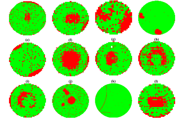
We extract twelve wafer maps from a public dataset that is widely cited in the semiconductor manufacturing community [54, 55]. While the original dataset contains a large number of wafer maps, we select twelve wafers so as to (1) reflect different mixed-type defect patterns of various complexity, and (2) to resemble as close as possible to the six wafer maps analyzed by [3] (which we do not have access to) in order to provide a fair comparison of our proposed approach relative to the state-of-art approach in the literature. Figure 4 displays the twelve chosen wafer maps, where the red and green squares depict the defective and functional chips, respectively.
III-B Results and Discussion
Hereinafter, we denote our proposed approach as AC-iWMM where adjacency-clustering for spatial filtering is coupled with the infinite warping mixture model for spatial clustering. The benchmark in comparison is the state-of-the-art filtering approach in [3], which is denoted hereinafter as CPF-iWMM where the connected path filtering (CPF) algorithm for spatial filtering is followed by iWMM for spatial clustering. Therefore, the fundamental difference between our approach and the benchmark lies in the spatial filtering stage, for which the impact on the quality of SPR is shown to be instrumental.
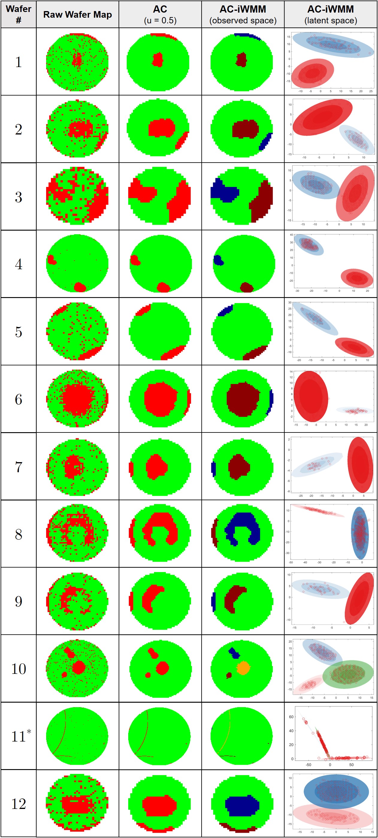
We test the AC model with a king-move neighborhood system, and standardize (i.e., ) for all , and set for all . The value of thus controls the spatial filtering level. In theory, we can choose the value of through a cross validation procedure as described by [43]. As discussed in subsection II-A, having a too large or too small value of is not ideal for the spatial filtering. We observe that for almost all defect patterns, the choice of achieves a sensible trade-off between the deviation and separation costs, and consistently yields superior performance in filtering various defect pattern combinations. This is in contrast to CPF for which there does not appear to be a value for its main parameter that works universally well for different defect types (findings to be discussed in the sequel). We implement the CPF algorithm following the description of the method by [3], while for iWMM, we adapt the codes available in [53]. Figure 5 shows the results of the AC-iWMM approach for a subset of the wafers, starting from the raw map, to AC-filtered results, to the clustering results in both the original and latent spaces. The visual results for all wafers are shown in Figure 10 in the Appendix.
III-B1 Visual Comparisons
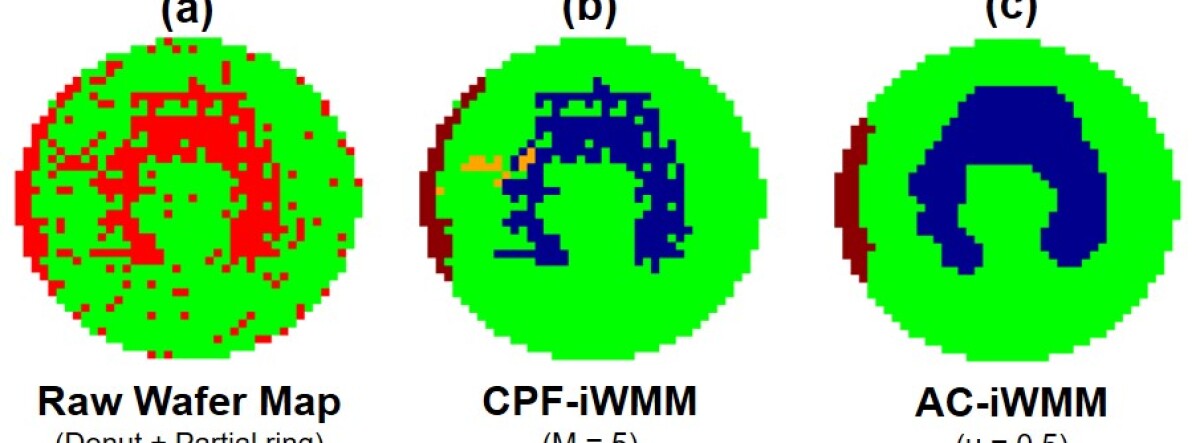
Before we present the quantitative results, we first draw some insights based on visual comparisons between our approach and the benchmark, CPF-iWMM. Figures 6 and 7 show the results of both approaches on two wafer maps. The first wafer map, illustrated in Figure 6, hosts donut and partial ring defect patterns. By virtue of AC filtering, iWMM is able to distinguish the two types of defects into two separate sub-clusters that are spatially distinct. This is achieved by correctly smoothing out the random noises between the two patterns with the use of local neighborhood information. In contrast, CPF mistakenly identifies some chips located in proximity to both sub-clusters as a separate sub-cluster, as it overlooks local neighborhood information. We note that iWMM was run at the same parameter settings for AC-iWMM and CFP-iWMM so the difference between the two sets of results is solely attributed to the spatial filtering approach.
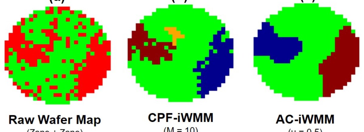
Another illustrative example is shown in Figure 7, in which the wafer map exhibits two zone defects. Again, CPF fails to separate the two sets of defective chips, causing iWMM to mistakenly flag a new separate sub-cluster. This is in contrast to AC-iWMM which yields a clear distinction between the two sub-clusters. We note that this problem cannot be alleviated by simply tuning the value of because the set of chips that are mistakenly flagged by CPF-iWMM are connected to one of the true sub-clusters, and hence, CPF will always treat it as one connected path. AC-iWMM does not keep this set of chips after AC filtering because the neighborhood information is utilized to smooth them out, reducing potential mishaps in the subsequent iWMM clustering stage.
III-B2 Quantitative Comparisons:
The clustering results obtained by both approaches are then evaluated using two sets of performance metrics that are known in the SPR literature as internal and external indices [56]. Assuming and are the sets of predicted and true cluster assignments, respectively, internal indices assess SPR quality when the underlying ground truth is not available, that is, without access to the set . External indices, on the other hand, make use of to validate the estimated SPR results.
Let us denote by the center of all coordinates in . Similarly, denotes the center of the coordinates in , i.e., the coordinates of the observations assigned to the th sub-cluster (for which ). Two widely recognized internal indices are the Calinski-Harabasz (CH) index and the Generalized Dunn index. The Calinski-Harabasz (CH) index calculates a weighted ratio of between-cluster and within-cluster dispersion and is defined in Eq. (7) [57]. By definition, a higher value for the CH index indicates a better performance.
| (7) |
where is the Euclidean norm, and is the predicted number of sub-clusters.
The Generalized Dunn Index (GDI) defines a similar ratio, as expressed in Eq. (8) [58]. A higher value for GDI indicates a better performance.
| (8) |
In addition to these internal indices, we test the performance of our approach on a set of widely recognized external indices. The motivation is that, in practice, domain experts can provide the ground truth for a set of testing wafer data which can be used to assess the performance of the competing SPR approaches. Since our dataset does not have the “ground truth,” or in other words the set , we reconstruct the ground truth by applying a pattern reconstruction technique which iterates over every pixel of the raw map and updates its value using a weighted sum of its surrounding pixels to generate an output image [59]. For our application, we used a neighborhood system with weight. We also observed that this weight selection had minimal impacts on the final results.
Three prevalent external indices are the Rand index (RI), adjusted Rand index (ARI), and normalized mutual information (NMI). The first two metrics are based on counting pairs of observations on which the predicted clustering results agree or disagree with the true clustering assignment. Specifically, let us assume that and are the true and predicted number of sub-clusters, respectively, and that denote the number of observations that are common in the th sub-cluster of and the th sub-cluster of . Now, let us define as the number of pairs pertaining to the same sub-cluster in and to the same sub-cluster in , while , on the other hand, denotes the number of pairs pertaining to different sub-clusters in and different sub-clusters in . With the above notations, RI, first introduced in [60], can be defined as:
| (9) |
where in case of perfect clustering, RI = 1, and in general, the higher its value, the better.
The second metric is the adjusted Rand index, or in short ARI, and is computed as follows:
| (10) |
where denotes the number of pairs pertaining to the same sub-cluster in and to different sub-clusters in , while, denotes the number of pairs pertaining to different sub-clusters in and to the same sub-cluster in . Similar to RI, a higher value of ARI indicates better performance.
The third external metric is NMI [61], which is an information-theoretic metric that measures the amount of information that and share, and is expressed as in Eq. (12). NMI ranges between and , with higher values indicating better performance.
| (11) |
such that
| (12) |
| CH () | GDI () | |||||
| Wafer # | CPF-iWMM (M=5) | CPF-iWMM (M=10) | AC-iWMM (u=0.50) | CPF-iWMM (M=5) | CPF-iWMM (M=10) | AC-iWMM (u=0.50) |
| 1 | 539.0 | 539.0 | 703.0 | .195 | .195 | .195 |
| 2 | 99.0 | 99.0 | 304.4 | .045 | .045 | .281 |
| 3 | 517.4 | 307.3 | 593.4 | .229 | .176 | .223 |
| 4 | 7800.5 | 7800.5 | 8266.1 | .303 | .303 | .300 |
| 5 | 1302.5 | 1214.6 | 1565.8 | .210 | .213 | .215 |
| 6 | 85.1 | 219.3 | 254.8 | .160 | .285 | .302 |
| 7 | 185.9 | 185.9 | 222.8 | .276 | .276 | .276 |
| 8 | 102.3 | 91.8 | 148.4 | .167 | .139 | .260 |
| 9 | 114.2 | 200.4 | 240.8 | .208 | .302 | .320 |
| 10 | 455.8 | 341.9 | 682.3 | .130 | .141 | .228 |
| 11* | 38.8 | 137.9 | 54.7 | .011 | .226 | .184 |
| 12 | 190.4 | 176.1 | 218.0 | .236 | .284 | .285 |
| RI () | ARI () | NMI () | |||||||
| Wafer # | CPF-iWMM (M=5) | CPF-iWMM (M=10) | AC-iWMM (u=0.50) | CPF-iWMM (M=5) | CPF-iWMM (M=10) | AC-iWMM (u=0.50) | CPF-iWMM (M=5) | CPF-iWMM (M=10) | AC-iWMM (u=0.50) |
| 1 | .969 | .969 | .985 | .938 | .938 | .970 | .877 | .877 | .916 |
| 2 | .927 | .927 | .956 | .849 | .849 | .908 | .785 | .785 | .845 |
| 3 | .831 | .830 | .856 | .612 | .607 | .661 | .660 | .647 | .686 |
| 4 | .993 | .993 | .990 | .986 | .986 | .979 | .950 | .950 | .936 |
| 5 | .976 | .974 | .985 | .952 | .948 | .969 | .897 | .893 | .917 |
| 6 | .900 | .901 | .943 | .772 | .776 | .869 | .751 | .770 | .841 |
| 7 | .940 | .940 | .967 | .877 | .877 | .932 | .817 | .817 | .876 |
| 8 | .919 | .922 | .939 | .837 | .842 | .877 | .762 | .778 | .812 |
| 9 | .872 | .871 | .923 | .726 | .724 | .830 | .699 | .711 | .790 |
| 10 | .977 | .973 | .980 | .954 | .946 | .961 | .888 | .880 | .906 |
| 11* | .985 | .987 | .985 | .968 | .971 | .968 | .938 | .946 | .936 |
| 12 | .894 | .885 | .931 | .775 | .759 | .851 | .743 | .738 | .799 |
Tables I and II summarize the comparison results, in terms of internal and external metrics, respectively. We have included results of the CPF approach at two different values of the threshold, namely and . With a lack of a systematic way to select , those two values are selected as representatives of a low and high value, respectively. All internal and external metrics are computed using the statistical programming software R. Specifically, values of RI and ARI are computed by using functionalities in the library fossil [62], while NMI is computed by calling the library NMI. All internal indices are computed by using functionalities in the library clusterCrit [63].
As shown in Tables I and II, we find that, in all wafers and across all metrics, AC-iWMM either outperforms or comes as a close second relative to CPF-iWMM with or . We also note that the performance of the CPF approach is, in many cases, sensitive to the choice of . As a case in point, varying from to in wafer #6 changes an internal metric like CH by as much as %, and an external metric like NMI by up to %. More importantly, there is not a choice of that consistently outperforms the other. For instance, we note that a choice of for wafer #3 outperforms that of . In contrast, a choice of for wafer # 6 renders consistently better results than across all metrics. This suggests that the choice of may be wafer-specific and requires expert judgment (as acknowledged in [3]). As opposed to CPF, the choice of for AC is shown to provide consistently satisfactory performance across all defect combinations, except for the scratch patterns, where a value of worked best. Note that, in principle, CPF is expected to perform considerably well in scratch patterns, since by design, scratch patterns are line defects, which, if longer than a carefully selected threshold (for this wafer, ), can be naturally characterized by CPF. Nevertheless, our approach is still able to effectively distinguish the scratch defects as shown in the visual results in Figure 10 (wafer #11). We also note how changing from to for this wafer results in a substantial deterioration in performance for CPF, as shown in Tables I and II.
| Internal Indices | External Indices | |||||||||
| CH | GDI | RI | ARI | NMI | ||||||
| Wafer # | M = 5 | M = 10 | M = 5 | M = 10 | M = 5 | M = 10 | M = 5 | M = 10 | M = 5 | M = 10 |
| 1 | 30.4% | 30.4% | 0.00% | 0.00% | 1.65% | 1.65% | 3.41% | 3.41% | 4.45% | 4.45% |
| 2 | 208% | 208% | 524% | 524% | 3.13% | 3.13% | 6.95% | 6.95% | 7.64% | 7.64% |
| 3 | 14.7% | 93.1% | -2.62% | 26.7% | 3.01% | 3.13% | 8.01% | 8.90% | 3.94% | 6.03% |
| 4 | 5.97% | 5.97% | -0.99% | -0.99% | -0.30% | -0.30% | -0.71% | -0.71% | -1.47% | -1.47% |
| 5 | 20.2% | 28.9% | 2.38% | 0.94% | 0.92% | 1.13% | 1.79% | 2.22% | 2.23% | 2.69% |
| 6 | 199% | 16.2% | 88.8% | 5.96% | 4.78% | 4.66% | 12.6% | 12.0% | 12.0% | 9.22% |
| 7 | 19.9% | 19.9% | -0.32% | -0.32% | 2.87% | 2.87% | 6.27% | 6.27% | 7.22% | 7.22% |
| 8 | 45.0% | 61.7% | 55.7% | 87.1% | 2.18% | 1.84% | 4.78% | 4.16% | 6.56% | 4.37% |
| 9 | 111% | 20.1% | 53.9% | 5.96% | 5.85% | 5.97% | 14.3% | 14.6% | 13.0% | 11.1% |
| 10 | 50.1% | 100% | 75.2% | 61.68% | 0.32% | 0.77% | 0.66% | 1.58% | 1.95% | 2.95% |
| 11 | 41.1% | -60.29% | 1594% | -18.6% | 0.00% | -0.20% | 0.00% | -0.42% | -0.30% | -1.10% |
| 12 | 14.5% | 23.82% | 20.31% | 0.20% | 4.16% | 5.17% | 9.77% | 12.11% | 7.62% | 8.31% |
| Avg. | 63.3% | 45.6% | 201% | 58.0% | 2.36% | 2.49% | 5.66% | 5.93% | 5.40% | 5.12% |
Table III presents the percentage improvements of AC-iWMM relative to CPF-iWMM at , , for all metrics. On average (last row of Table III), AC-iWMM achieves an average improvement of up to % over CPF-iWMM in terms of internal metrics, and up to % in terms of external metrics. The difference in scale between the improvements in internal and external indices is attributed to how these metrics are defined in the first place; As described earlier, internal metrics are used to assess the clustering quality sans externally provided information about the underlying cluster labels. While external validation metrics are perhaps more interpretable than their internal counterparts, the latter can be extremely useful in practice, since it may be cumbersome for experts to constantly weigh in and provide external information about class labels for all tested wafers. In other words, internal validation provides an automated check point to evaluate the method’s performance in real-time. To confirm the considerable improvement brought by AC-iWMM, we perform the Wilcoxon signed ranked test, which is a nonparametric statistical test of hypothesis, with its null hypothesis suggesting that the difference between a pair of samples follows a symmetric zero-centered distribution. The resulting -values are shown in Table IV, wherein improvements are shown to be statistically significant for all metrics at a significance level of , except for improvements in GDI which are significant at a significance level.
| Internal Indices | External Indices | ||||||||
|---|---|---|---|---|---|---|---|---|---|
| CH | GDI | RI | ARI | NMI | |||||
| M = 5 | M = 10 | M = 5 | M = 10 | M = 5 | M = 10 | M = 5 | M = 10 | M = 5 | M = 10 |
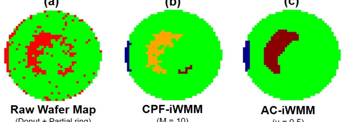
Another interesting observation is the magnitude of improvement realized by AC-iWMM over CPF-iWMM as a function of the defect pattern complexity. Specifically, we note that improvements from AC-iWMM are more pronounced for more complex-shaped defect patterns, and are diminishing as the defect patterns become relatively simpler. For instance, substantial improvements (maximal for some metrics) in Tables I and II come from wafer map #9, hosting donut and partial ring defect patterns. The results for that wafer is shown in Figure 8. Understandably, donut and partial ring defect patterns are, by design, intricate shapes, making the distinction between random and systematic defects a much harder task. This is where the AC approach, through exploiting the local spatial information, can play an instrumental role in improving the quality of the spatial filtering step, and eventually, the downstream clustering and pattern recognition. On the other hand, CPF does not make use of local neighborhood information, which causes the downstream clustering to misidentify several defective chips as an independent sub-cluster.
In contrast, wafer map #4 has a relatively simple mixed-type defect pattern, in which the two zone defects are round shaped and far from each other. Furthermore, the random defects outside the two zones are relatively sparse, which makes the filtering task straightforward. Therefore, both methods were able to produce satisfactory performance, with almost negligible visual differences, as shown in Figure 9.
The observations from Figures 8 (for wafer map #9) and 9 (for wafer map #4) validate our conjecture that the difference in performance of AC-iWMM relative to CPF-iWMM hinges on the complexity of the underlying defect patterns. A closer look at the results in Table III suggests the same observation for wafer maps #6 (visual result shown in Figure 10 in the Appendix) and #8 (visual result shown in Figure 6), which have complex-shaped patterns, and hence, the benefit from AC-iWMM appears to be more pronounced. As the wafer fabrication process grows in scale and sophistication, owing to technology upgrades, or an increase in the number of processing steps or the density of chips per wafer, wafers are expected to exhibit more intricate and mixed-type defect patterns. Thus, we anticipate that our proposed approach will generate even more profound impacts.
IV Conclusions
In this paper we have proposed a spatial pattern recognition framework (AC-iWMM) for detecting mixed-type defect patterns in wafer bin map data—a problem of vital importance to ensuring quality control in the semiconductor manufacturing industry. This framework integrates the adjacency-clustering (AC) model for spatial filtering with an advanced mixture model (iWMM) for spatial clustering. AC has a desirable combinatorial structure and can be solved in polynomial time by a minimum-cut algorithm. By utilizing the local neighborhood information, AC is able to effectively distinguish the systematic patterns from random noises. As a result, iWMM, which subsequently acts on the AC-filtered data, can properly cluster the systematic patterns into different types. We validate the superior performance of AC-iWMM on twelve real-world wafer bin maps exhibiting different mixed-type defect patterns. Based on both visual and quantitative comparisons, AC-iWMM outperforms the state-of-the-art method in the literature, especially for complex-shaped, mixed-type patterns.
The framework proposed herein can be extended in various directions. One interesting idea is to incorporate additional features to aid with mixed-type SPR such as the number of defects per bin on the premise that defects due to the same assignable cause may exhibit similar defect severity levels. Incorporating this information will drive a departure from using binary wafer maps, which, by consequence, will require a new definition of what constitutes a cluster in our setting.
Appendix A Additional details about iWMM
Here we provide additional details about iWMM, which was initially proposed by [50]. iWMM comprises two building blocks: (1) a warping function to match the observed spatial locations of the AC-filtered results, denoted by , with a set of latent spatial coordinates in a latent space, denoted by , and (2) a clustering method which determines the clustering assignments in in the latent space, denoted by . While in theory, can have a different dimensionality than , it suffices in our setting to assume that both .
As a warping function, a Gaussian process latent variable model (GPLVM) [51] with squared exponential covariance, is used, and can be expressed as in Eq. (5). Then, the infinite Gaussian mixture model (iGMM) is used for spatial clustering, and is expressed as in Eq. (6). For iGMM, a Gaussian-Wishart prior is placed on its parameters and , such that:
| (13) |
where is the Wishart distribution. The parameters , are the mean and relative precision of , respectively, while and are the scale matrix for , and its degree of freedom, respectively. One can then derive the probability distribution of given the clustering assignments by integrating out and , as in Eq. (14).
| (14) |
where is the number of chips assigned to the th sub-cluster, while , , and are the posterior Gaussian-Wishart parameters of the th component (or sub-cluster), such that , , and , with .
A Dirichlet process prior with concentration parameter is used for infinite mixture modeling in the latent space. Then, the probability distribution of can be written as:
| (15) |
Collecting the above pieces, the joint distribution of , , and conditional on all parameters, can be written as:
| (16) |
which is merely the product of the terms determined by Eqs. (5), (14), and (15).
The authors in [50] provide a detailed procedure to fit the iWMM to a set of observed spatial locations , where the latent coordinates , assignments , as well as remaining parameters are inferred through a Markov Chain Monte Carlo (MCMC)-based procedure. The procedure consists of two steps, which are repeatedly performed until convergence. The first step entails a Gibbs sampling scheme of the latent assignment of the th chip, denoted by , from the following probability distribution:
| (17) |
where is the set of latent coordinates of the th sub-cluster, excluding the th chip. Similarly, is the set of assignments, excluding that of the th chip, and is the number of chips assigned to the th sub-cluster, excluding the th chip. The probability distributions in the right hand-side of Eq. (17) can be analytically derived in closed-form as detailed in [50]. The second step entails sampling the latent coordinates from the probability distribution using hybrid Monte Carlo. Combined, the two steps yield an estimate of the posterior distribution of the latent coordinates and the latent assignments .
Appendix B Clustering results for all wafers
Appendix C
Acknowledgment
The research of Dorit S. Hochbaum is supported in part by NSF award No. CMMI-1760102.
References
- [1] K. S. El-Kilany, “Reusable modelling and simulation of flexible manufacturing for next generation semiconductor manufacturing facilities,” Ph.D. dissertation, Dublin City School. School of Mechanical and Manufacturing Engineering, 2003.
- [2] J. Y. Hwang and W. Kuo, “Model-based clustering for integrated circuit yield enhancement,” European Journal of Operational Research, vol. 178, no. 1, pp. 143–153, 2007.
- [3] J. Kim, Y. Lee, and H. Kim, “Detection and clustering of mixed-type defect patterns in wafer bin maps,” IISE Transactions, vol. 50, no. 2, pp. 99–111, 2018.
- [4] S. P. Cunningham and S. Mackinnon, “Statistical methods for visual defect metrology,” IEEE Transactions on Semiconductor Manufacturing, vol. 11, no. 1, pp. 48–53, 1998.
- [5] S. Neo, A. Quah, G. Ang, D. Nagalingam, H. Ma, S. Ting, C. Soo, C. Chen, Z. Mai, and J. Lam, “Failure analysis methodology on donut pattern failure due to photovoltaic electrochemical effect,” Microelectronics Reliability, vol. 76, pp. 255–260, 2017.
- [6] G. Tello, O. Y. Al-Jarrah, P. D. Yoo, Y. Al-Hammadi, S. Muhaidat, and U. Lee, “Deep-structured machine learning model for the recognition of mixed-defect patterns in semiconductor fabrication processes,” IEEE Transactions on Semiconductor Manufacturing, vol. 31, no. 2, pp. 315–322, 2018.
- [7] K. Kyeong and H. Kim, “Classification of mixed-type defect patterns in wafer bin maps using convolutional neural networks,” IEEE Transactions on Semiconductor Manufacturing, vol. 31, no. 3, pp. 395–402, 2018.
- [8] Y. Kong and D. Ni, “Recognition and location of mixed-type patterns in wafer bin maps,” in 2019 IEEE International Conference on Smart Manufacturing, Industrial & Logistics Engineering (SMILE). IEEE, 2019, pp. 4–8.
- [9] H. Lee and H. Kim, “Semi-supervised multi-label learning for classification of wafer bin maps with mixed-type defect patterns,” IEEE Transactions on Semiconductor Manufacturing, 2020, accepted.
- [10] J. Wang, C. Xu, Z. Yang, J. Zhang, and X. Li, “Deformable convolutional networks for efficient mixed-type wafer defect pattern recognition,” IEEE Transactions on Semiconductor Manufacturing, 2020, accepted.
- [11] T. Yuan and W. Kuo, “A model-based clustering approach to the recognition of the spatial defect patterns produced during semiconductor fabrication,” IIE Transactions, vol. 40, no. 2, pp. 93–101, 2007.
- [12] ——, “Spatial defect pattern recognition on semiconductor wafers using model-based clustering and Bayesian inference,” European Journal of Operational Research, vol. 190, no. 1, pp. 228–240, 2008.
- [13] T. Yuan, W. Kuo, and S. J. Bae, “Detection of spatial defect patterns generated in semiconductor fabrication processes,” IEEE Transactions on Semiconductor Manufacturing, vol. 24, no. 3, pp. 392–403, 2011.
- [14] C. H. Jin, H. J. Na, M. Piao, G. Pok, and K. H. Ryu, “A novel DBSCAN-based defect pattern detection and classification framework for wafer bin map,” IEEE Transactions on Semiconductor Manufacturing, vol. 32, no. 3, pp. 286–292, 2019.
- [15] C.-H. Wang, “Separation of composite defect patterns on wafer bin map using support vector clustering,” Expert Systems with Applications, vol. 36, no. 2, pp. 2554–2561, 2009.
- [16] L.-C. Chao and L.-I. Tong, “Wafer defect pattern recognition by multi-class support vector machines by using a novel defect cluster index,” Expert Systems with Applications, vol. 36, no. 6, pp. 10 158–10 167, 2009.
- [17] W. Taam and M. Hamada, “Detecting spatial effects from factorial experiments: An application from integrated-circuit manufacturing,” Technometrics, vol. 35, no. 2, pp. 149–160, 1993.
- [18] Y.-S. Jeong, S.-J. Kim, and M. K. Jeong, “Automatic identification of defect patterns in semiconductor wafer maps using spatial correlogram and dynamic time warping,” IEEE Transactions on Semiconductor Manufacturing, vol. 21, no. 4, pp. 625–637, 2008.
- [19] K. Taha, K. Salah, and P. D. Yoo, “Clustering the dominant defective patterns in semiconductor wafer maps,” IEEE Transactions on Semiconductor Manufacturing, vol. 31, no. 1, pp. 156–165, 2017.
- [20] K. P. White, B. Kundu, and C. M. Mastrangelo, “Classification of defect clusters on semiconductor wafers via the hough transformation,” IEEE Transactions on Semiconductor Manufacturing, vol. 21, no. 2, pp. 272–278, 2008.
- [21] Y. Liu and S. Zhou, “Detecting point pattern of multiple line segments using hough transformation,” IEEE Transactions on Semiconductor Manufacturing, vol. 28, no. 1, pp. 13–24, 2014.
- [22] B. Kim, Y.-S. Jeong, S. H. Tong, I.-K. Chang, and M.-K. Jeongyoung, “A regularized singular value decomposition-based approach for failure pattern classification on fail bit map in a dram wafer,” IEEE Transactions on Semiconductor Manufacturing, vol. 28, no. 1, pp. 41–49, 2015.
- [23] R. Wang and N. Chen, “Wafer map defect pattern recognition using rotation-invariant features,” IEEE Transactions on Semiconductor Manufacturing, vol. 32, no. 4, pp. 596–604, 2019.
- [24] M. Piao, C. H. Jin, J. Y. Lee, and J.-Y. Byun, “Decision tree ensemble-based wafer map failure pattern recognition based on radon transform-based features,” IEEE Transactions on Semiconductor Manufacturing, vol. 31, no. 2, pp. 250–257, 2018.
- [25] J. Yu and X. Lu, “Wafer map defect detection and recognition using joint local and nonlocal linear discriminant analysis,” IEEE Transactions on Semiconductor Manufacturing, vol. 29, no. 1, pp. 33–43, 2015.
- [26] F. Adly, P. D. Yoo, S. Muhaidat, Y. Al-Hammadi, U. Lee, and M. Ismail, “Randomized general regression network for identification of defect patterns in semiconductor wafer maps,” IEEE Transactions on Semiconductor Manufacturing, vol. 28, no. 2, pp. 145–152, 2015.
- [27] M. Saqlain, B. Jargalsaikhan, and J. Y. Lee, “A voting ensemble classifier for wafer map defect patterns identification in semiconductor manufacturing,” IEEE Transactions on Semiconductor Manufacturing, vol. 32, no. 2, pp. 171–182, 2019.
- [28] F.-L. Chen and S.-F. Liu, “A neural-network approach to recognize defect spatial pattern in semiconductor fabrication,” IEEE Transactions on Semiconductor Manufacturing, vol. 13, no. 3, pp. 366–373, 2000.
- [29] C.-T. Su, T. Yang, and C.-M. Ke, “A neural-network approach for semiconductor wafer post-sawing inspection,” IEEE Transactions on Semiconductor Manufacturing, vol. 15, no. 2, pp. 260–266, 2002.
- [30] F. Di Palma, G. De Nicolao, G. Miraglia, E. Pasquinetti, and F. Piccinini, “Unsupervised spatial pattern classification of electrical-wafer-sorting maps in semiconductor manufacturing,” Pattern Recognition Letters, vol. 26, no. 12, pp. 1857–1865, 2005.
- [31] C.-J. Huang, “Clustered defect detection of high quality chips using self-supervised multilayer perceptron,” Expert Systems with Applications, vol. 33, no. 4, pp. 996–1003, 2007.
- [32] C.-W. Liu and C.-F. Chien, “An intelligent system for wafer bin map defect diagnosis: An empirical study for semiconductor manufacturing,” Engineering Applications of Artificial Intelligence, vol. 26, no. 5-6, pp. 1479–1486, 2013.
- [33] C.-F. Chien, S.-C. Hsu, and Y.-J. Chen, “A system for online detection and classification of wafer bin map defect patterns for manufacturing intelligence,” International Journal of Production Research, vol. 51, no. 8, pp. 2324–2338, 2013.
- [34] H. Lee, Y. Kim, and C. O. Kim, “A deep learning model for robust wafer fault monitoring with sensor measurement noise,” IEEE Transactions on Semiconductor Manufacturing, vol. 30, no. 1, pp. 23–31, 2016.
- [35] T. Nakazawa and D. V. Kulkarni, “Wafer map defect pattern classification and image retrieval using convolutional neural network,” IEEE Transactions on Semiconductor Manufacturing, vol. 31, no. 2, pp. 309–314, 2018.
- [36] N. Yu, Q. Xu, and H. Wang, “Wafer defect pattern recognition and analysis based on convolutional neural network,” IEEE Transactions on Semiconductor Manufacturing, vol. 32, no. 4, pp. 566–573, 2019.
- [37] K. Imoto, T. Nakai, T. Ike, K. Haruki, and Y. Sato, “A CNN-based transfer learning method for defect classification in semiconductor manufacturing,” IEEE Transactions on Semiconductor Manufacturing, vol. 32, no. 4, pp. 455–459, 2019.
- [38] Y. Kong and D. Ni, “A semi-supervised and incremental modeling framework for wafer map classification,” IEEE Transactions on Semiconductor Manufacturing, vol. 33, no. 1, pp. 62–71, 2020.
- [39] J. Hwang and H. Kim, “Variational deep clustering of wafer map patterns,” IEEE Transactions on Semiconductor Manufacturing, vol. 33, no. 3, pp. 466–475, 2020.
- [40] T.-H. Tsai and Y.-C. Lee, “A light-weight neural network for wafer map classification based on data augmentation,” IEEE Transactions on Semiconductor Manufacturing, 2020, accepted.
- [41] J. Jang, M. Seo, and C. O. Kim, “Support weighted ensemble model for open set recognition of wafer map defects,” IEEE Transactions on Semiconductor Manufacturing, 2020, accepted.
- [42] Y. Hyun and H. Kim, “Memory-augmented convolutional neural networks with triplet loss for imbalanced wafer defect pattern classification,” IEEE Transactions on Semiconductor Manufacturing, 2020, accepted.
- [43] D. S. Hochbaum and S. Liu, “Adjacency-clustering and its application for yield prediction in integrated circuit manufacturing,” Operations Research, vol. 66, no. 6, pp. 1571–1585, 2018.
- [44] H. Rue and L. Held, Gaussian Markov Random Fields: Theory and Applications. Chapman and Hall/CRC, 2005.
- [45] S. Geman and C. Graffigne, “Markov random field image models and their applications to computer vision,” in Proceedings of the International Congress of Mathematicians, vol. 1. Berkeley, CA, 1986, pp. 1496–1517.
- [46] M. H. Hansen, V. N. Nair, and D. J. Friedman, “Monitoring wafer map data from integrated circuit fabrication processes for spatially clustered defects,” Technometrics, vol. 39, no. 3, pp. 241–253, 1997.
- [47] L. Bao, K. Wang, and R. Jin, “A hierarchical model for characterising spatial wafer variations,” International Journal of Production Research, vol. 52, no. 6, pp. 1827–1842, 2014.
- [48] D. S. Hochbaum, “An efficient algorithm for image segmentation, markov random fields and related problems,” Journal of the ACM (JACM), vol. 48, no. 4, pp. 686–701, Jul. 2001.
- [49] R. K. Ahuja, D. S. Hochbaum, and J. B. Orlin, “Solving the convex cost integer dual network flow problem,” Management Science, vol. 49, no. 7, pp. 950–964, 2003.
- [50] T. Iwata, D. Duvenaud, and Z. Ghahramani, “Warped mixtures for nonparametric cluster shapes,” arXiv preprint arXiv:1206.1846, 2012.
- [51] N. D. Lawrence, “Gaussian process latent variable models for visualisation of high dimensional data,” in Advances in Neural Information Processing Systems, 2004, pp. 329–336.
- [52] C. K. Williams and C. E. Rasmussen, Gaussian Processes for Machine Learning. MIT Press Cambridge, MA, 2006.
- [53] T. Iwata and D. Duvenaud, “Code for inferring nonparametric cluster shapes using warped mixtures,” https://github.com/duvenaud/warped-mixtures, 2016.
- [54] J.-S. R. Jang, “Wafer map dataset,” http://mirlab.org/dataSet/public/, 2014.
- [55] M.-J. Wu, J.-S. R. Jang, and J.-L. Chen, “Wafer map failure pattern recognition and similarity ranking for large-scale data sets,” IEEE Transactions on Semiconductor Manufacturing, vol. 28, no. 1, pp. 1–12, 2014.
- [56] O. Arbelaitz, I. Gurrutxaga, J. Muguerza, J. M. Pérez, and I. Perona, “An extensive comparative study of cluster validity indices,” Pattern Recognition, vol. 46, no. 1, pp. 243–256, 2013.
- [57] T. Caliński and J. Harabasz, “A dendrite method for cluster analysis,” Communications in Statistics-Theory and Methods, vol. 3, no. 1, pp. 1–27, 1974.
- [58] J. C. Bezdek and N. R. Pal, “Some new indexes of cluster validity,” IEEE Transactions on Systems, Man, and Cybernetics, Part B (Cybernetics), vol. 28, no. 3, pp. 301–315, 1998.
- [59] R. C. Gonzalez and R. E. Woods, Digital Image Processing. Prentice Hall, 2002.
- [60] W. M. Rand, “Objective criteria for the evaluation of clustering methods,” Journal of the American Statistical Association, vol. 66, no. 336, pp. 846–850, 1971.
- [61] N. X. Vinh, J. Epps, and J. Bailey, “Information theoretic measures for clusterings comparison: Variants, properties, normalization and correction for chance,” Journal of Machine Learning Research, vol. 11, pp. 2837–2854, 2010.
- [62] M. J. Vavrek, “Fossil: palaeoecological and palaeogeographical analysis tools,” Palaeontologia Electronica, vol. 14, no. 1, pp. 1–16, 2011.
- [63] B. Desgraupes, “Clustering indices,” University of Paris Ouest-Lab Modal’X, vol. 1, p. 34, 2013.