Extreme Lightwave Electron Field Emission from a Nanotip
Abstract
We report on sub-cycle terahertz light-field emission of electrons from tungsten nanotips under extreme conditions corresponding to a Keldysh parameter . Local peak THz fields up to 40 GV/m are achieved at the apex of an illuminated nanotip, causing sub-cycle cold-field electron emission and acceleration in the quasi-static field. By simultaneous measurement of the electron bunch charge and energy distribution, we perform a quantitative test of quasi-static Fowler-Nordheim tunnelling theory under field conditions that completely suppress the tunnel barrier. Very high bunch charges of electrons/pulse are observed, reaching maximum energies of 3.5 keV after acceleration in the local field. The energy distribution and emission current show good agreement with Fowler-Nordheim theory even in this extreme field regime. Extending this model to the single-shot regime under these conditions predicts peak electron distributions with a spectral purity of . THz field-induced reshaping and sharpening of the nanotip is observed, reducing the tip radius from 120 nm to 35 nm over roughly THz shots. These results indicate THz-driven nanotips in the extreme field limit are promising electron sources for ultrafast electron diffraction and microscopy.
Light-matter interactions enter the extreme limit when the energy scale of the field interaction meets or exceeds a characteristic excitation energy of the system [1, 2]. In electron photoemission from a metal surface, the relevant energy scale is the work function, typically a few eV. The electron surface potential is transiently tilted in a light field applied normal to the surface, permitting electrons to tunnel to the vacuum at a rate that depends exponentially on the field-dependent width of the barrier [3, 4]. The ratio of the tunnelling time to the period of the light field defines the Keldysh parameter, , and for the field interaction is quasi-static [5]. For near-infrared to visible light, the light intensities required to reach are on the order of W/cm2, exceeding the damage threshold of metals [6]. Quasi-static light-matter interactions in the solid state have subsequently been relatively unexplored.
Intense, single-cycle terahertz (THz) pulses illuminating metal nanotips provide a means to explore this extreme light-matter interaction regime [7, 8, 9, 10]. Localized to the tip apex, a broadband local field enhancement occurs via a lightning rod effect that scales as , where R is the nanotip radius and is the vacuum wavelength [9]. Intense single cycle THz pulses with peak electric fields of 1-10 MV/m become locally enhanced by to several GV/m at the nanotip surface. While such dc fields would immediately cause catastrophic damage, breakdown is strongly suppressed at higher frequencies under ac field conditions [11]. Moreover, under pulsed illumination the threshold field for breakdown scales with the pulse duration as [12].
These GV/m local fields exceed the threshold for sub-cycle cold-field emission from the metal nanotip [13, 14, 9, 15]. Field-emitted electrons drawn directly from the Fermi level are subsequently accelerated to several keV in the quasi-static field before leaving the local field enhancement region that decays over length scales comparable to the tip radius. Thus the electrons follow a deterministic path governed by the near instantaneous field under which they are ejected. These cold-field emitted electrons have potential applications as seeds for THz-based accelerators and sources for time-resolved electron diffraction [16] and time-resolved point-projection electron microscopy [17]. For many applications, particularly those seeking near single shot operation, electron bunch charges of electrons/pulse are typically required for simple, few atom unit cells [18]. Electron bunch charges up to 100 electrons/pulse have been reported from nanotips driven by mid-infrared pulses with [13]. We note that larger bunch charges were likely achieved, but not quantitatively measured, using low repetition rate, intense THz pulses [9].
In this work, we demonstrate sub-cycle THz field emission of electron pulses from a tungsten nanotip in the extreme field limit corresponding to , deep into the quasi-static regime. Average emission currents nA are measured corresponding to bunch charges of electrons/pulse. We simultaneously measure the electron energy distribution, with peak energies up to 3.5 keV, comparable to previous work [9]. We test this emission against quasi-static Fowler–Nordheim theory and find good agreement despite it being well beyond the limitations of the model. Finally, a pronounced sharpening of the nanotip is observed under these extreme field conditions, gradually reducing the size of the tip from its initial 120 nm radius to sub-35 nm over an estimated shots.
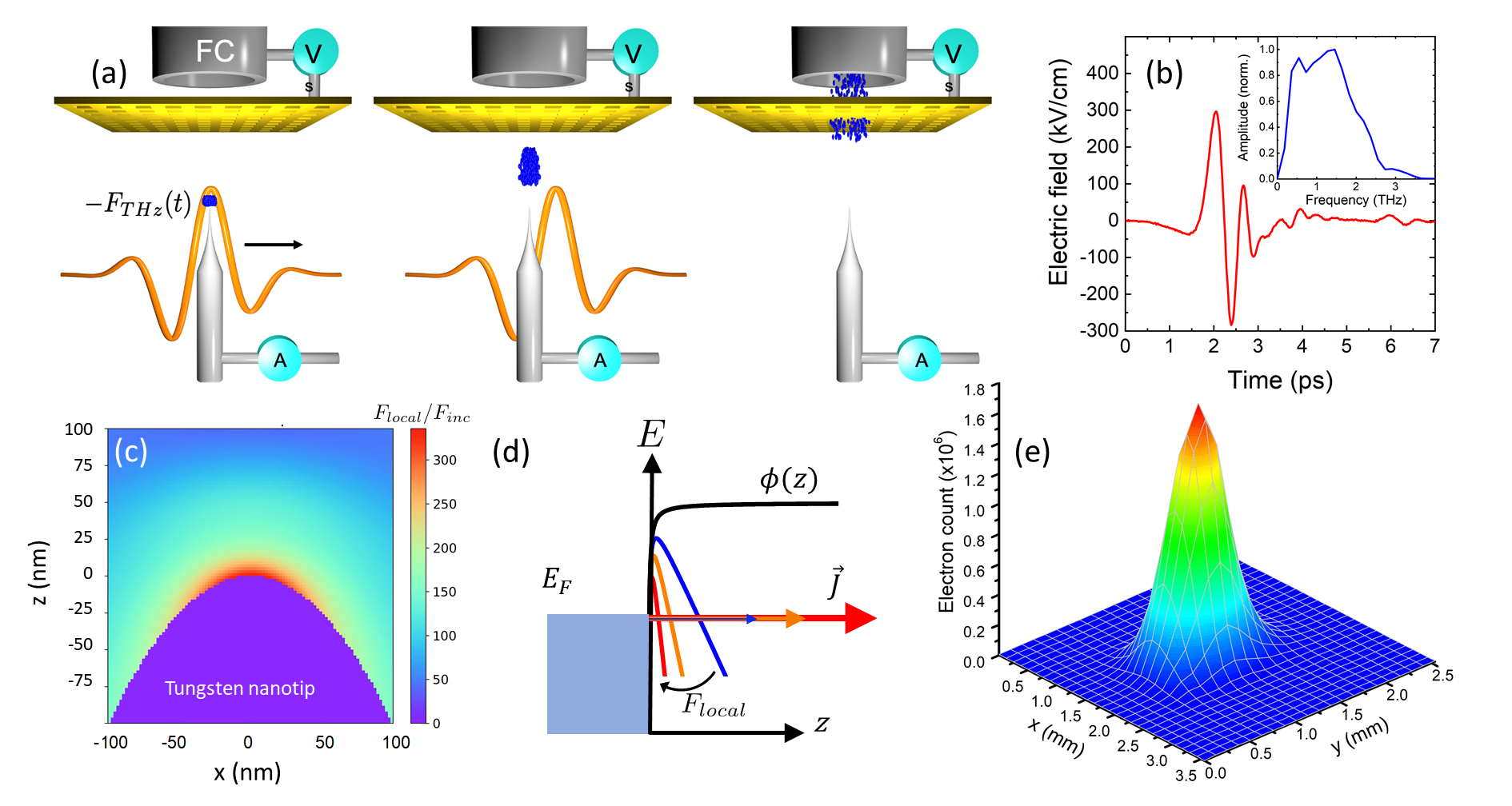
A schematic of the experiment is shown in Fig. 1(a). Single-cycle THz pulses are generated by tilted pulse-front optical rectification in a room temperature, MgO:LiNbO3 prism pumped by 800 nm, 4 mJ laser pulses of 120 fs duration at a 1 kHz repetition rate [19, 20]. Intense THz pulses are focused to a near diffraction–limited spot on a tungsten nanotip with linear polarization aligned to the nanotip axis, held within a small vacuum chamber with a base pressure of torr. Tips were prepared from a polycrystalline tungsten wire using standard electrochemical etching in a KOH solution [21]. The nanotip radius was initially 120 nm, as verified by scanning electron microscopy (See Fig. 4). The transmitted THz pulse is minimally perturbed by the presence of the nanotip and is 1:1 imaged on a 200 m-thick, (110)-cut GaP crystal for free-space electro-optic sampling of the THz field. The most intense THz waveform experienced by the tip is shown in Fig. 1(b) with its amplitude spectrum shown in the inset. The fields are calibrated assuming a GaP electro-optic coefficient pm/V [22], accounting for the Fresnel loss of the final high resistivity silicon vacuum chamber window. A pair of wire grid polarizers was used to vary the incident THz peak field strength without changing its polarization state. The tungsten nanotip can be actuated in all three directions inside the chamber through the THz focus over a several mm range by moving the nanotip holder coupled through a baffle.
The electron energy distribution and bunch charge are measured simultaneously via a Faraday cup detector positioned less than 1 cm away from the tip along the emission axis, with a varying stopping potential () applied to a grid placed before the detector. Additionally, an electrical connection is made to the tip allowing a direct measurement of the total current being drawn through the tip. These two currents are measured simultaneously using two Keithley 6517B electrometers.
Three dimensional finite–difference time–domain (FDTD) simulations were performed to model the local THz fields coupled to tungsten nanotips. The nanotip shape was approximated as a prolate spheroid, which allowed the expansion of the fields in spherical coordinates where the Helmholtz equation is separable [23]. Typical field enhancements of are calculated for a 50 nm radius tip, as shown in Fig. 1(c) using the input field given in Fig. 1(b) (see Supplemental Material [24]). While this dipole model qualitatively captures the decay of the local field enhancement away from the tip apex, it ignores the atomic scale structure of the tip and spatial texture in the local field that would be observed in a field ion microscopy image, for example. A more accurate estimation of the local field at the point of emission can be obtained from the measured energy distribution as discussed below.
Cold field emission of electrons from metal nanotips under dc and quasi-dc field conditions, depicted in Fig. 1(d), is typically described by Fowler-Nordheim theory [3]. The instantaneous local THz field, , tilts the electron potential given by the Schottky-Nordheim function
with eV being the work function of the tungsten tip. The critical field required to lower this potential barrier to zero relative to the Fermi energy is given by GV/m for tungsten [25]. The emission current is subsequently calculated via the tunneling probability through this barrier. The zero temperature Fowler-Nordheim equation for the current density J can then be written as
| (1) |
where a and b are Fowler-Nordheim constants. The function accounts for image charges and exponentially suppresses the emission, although is valid only for [26]. Since the influence of the image charges is limited to very close to the tip apex where local fields are the strongest, we find all data can be described by setting (see Supplemental Material [24]).
The total electron emission ( V) is shown in Fig. 1(e), measured using a direct electrical connection on the nanotip and scanning the tip through the focal plane of the THz pulse. Electron bunch charges in excess of electrons/pulse were measured on peak, more than three orders higher than previously reported [27, 13]. The relative THz/tip-position dependence of the field-emission current (bunch charge) follows an asymmetric Gaussian with FWHM of 580 m and 450 m in the x and y directions, respectively (Fig. 1(e)). These dimensions are comparable to those of the THz intensity distribution at the tip position as measured using a microbolometer camera. While Fowler-Nordheim emission predicts a sharpened distribution for due to the exponential dependence on the field, in the extreme limit of the exponential term saturates and the electron distribution is governed by , i.e. the intensity distribution. Thus both the large electron count rate and the Gaussian spatial distribution indicate that we are operating in the extreme limit of field emission.
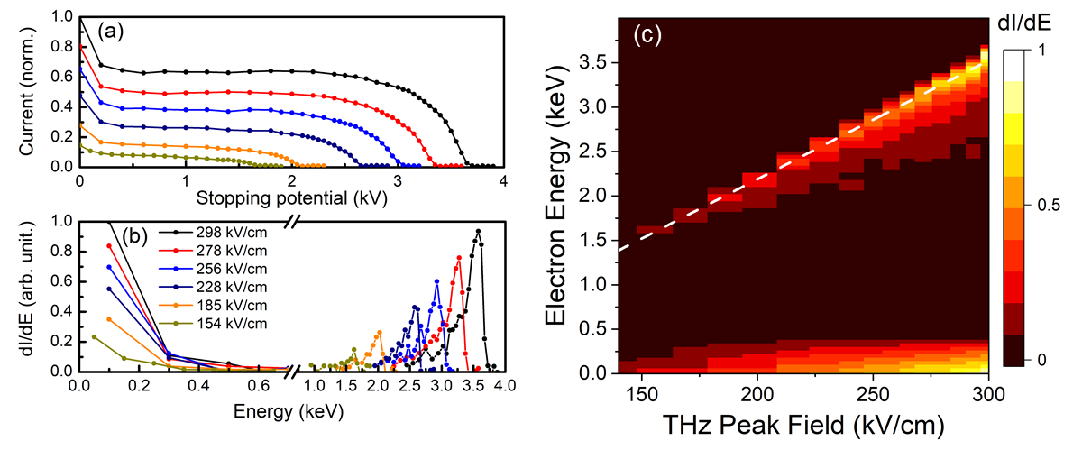
The normalized electron current from the Faraday cup is shown in Fig. 2(a) for varying peak incident THz field strength. The current shows a marked reduction at low potentials ( eV) and a high energy cutoff at several keV. We note the beam current could be manipulated by the presence of a permanent magnet brought close to the chamber, confirming the origin of these signals as a free-space electron beam. The numerical derivative of this spectra gives the energy distribution, whose low and high energy regions are shown in Figs. 2(b). The low energy distribution shows a monotonically decreasing distribution to a cutoff of approximately 400 eV, while the high energy distribution is sharply peaked at energies up to 3.5 keV. The origin of the low energy distribution is puzzling. Given the significant portion of electrons present in the low energy part of the distribution, these electrons must be field emitted during the peak of the THz field. Electrons emitted during this time would usually be accelerated ballistically to form the high energy peaked distribution. Evidently, a significant portion of electrons are not immediately swept out of the tip region but instead experience a lower accelerating THz field. Such a delayed photoemission channel has recently been demonstrated using few-cycle optical pulses, where re-scattered electrons are driven back to the nanotip surface by subsequent field cycles [28]. Inelastic scattering within the metal can result in delay of the electron emission by 10’s of fs. While this cannot explain our results, it points to the role of inelastic scattering during the emission process. A possible mechanism for such a significant low energy population is through interactions with surface contaminants. Initially emitted electrons can scatter within contaminant layers [29], subsequently becoming trapped. They can eventually escape and accelerate in a subsequent cycle of the THz field. Numerical simulations of THz resonances excited in the nanotip shows that a radially polarized, dispersionless Sommerfeld wave is launched on the nanotip [30, 31]. This wave reflects at the tip boundaries resulting in a multi-cycle field at a resonant frequency of where mm is the tip length. As the local field enhancement favours low frequencies (numerically , see Supplemental Material [24]), as does the ponderomotive energy , electrons can reach 400 eV in this multi-cycle field with as low as MV/m. The complete energy distribution is shown in Fig. 2(c). While the ponderomotive energy of trapped electrons should scale as , we observe saturation in the peak electron energy at eV. While the electron energy loss spectra of tungsten nitride shows no excitations in the 100-400 eV energy range, an onset of strong electron absorption above 400 eV coincides with the nitrogen 1s excitation [32, 33, 34]. We therefore assign the low energy distribution to electrons inelastically scattered within the nitride, delaying emission and accelerated by the Sommerfeld resonance of the tip. Further evidence for electron energy transfer to surface adsorbates is given later when we examine the nanoscale structure of the tip after long term exposure.
A linear field dependence of the high energy peak is observed in Fig. 2(c), as expected for ballistic acceleration. The peak energy is given by where is the effective length scale of the field enhancement. The linear fit (white dashed line) with a slope of 13.3 eV cm/kV = directly yields the local field enhancement factor for a nm, approximated as the tip radius. The in this simple estimate is as high as 115 V/nm, more than 8 times the critical field . The time scales for electrons to leave the field enhancement region is on the order of 5 fs, well within the quasi-static emission regime. The corresponding adiabaticity parameter , relating the near field decay length to the electron quiver amplitude, is also well within the quasi-static limit [13].
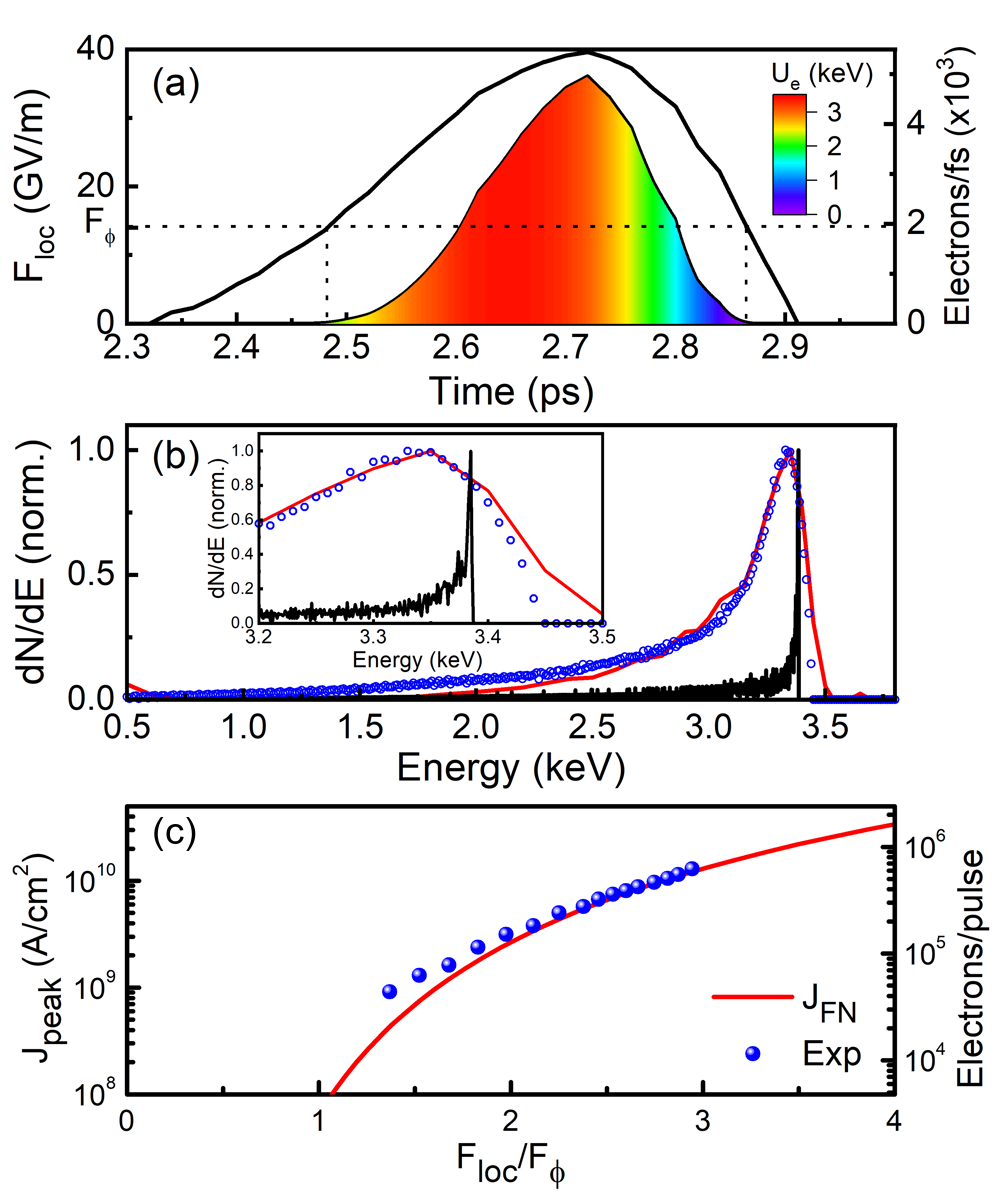
In the quasi-static limit, the Fowler-Nordheim (F-N) equations can simulate the emission dynamics of the high energy distribution. The emission current and final electron energy were calculated using a time-dependent, one dimensional finite-element simulation taking into account the near-field decay of a hyperboloidal tip , [9, 35] with and R=35 nm, the Gaussian THz field focus and the THz pulse waveform in Fig. 1(b). The high energy electrons rapidly leave the field enhancement region, however still experience the entire THz waveform before leaving the THz focal region. Electrons are only slightly slowed down by the subsequent field half-cycle before they escape the free-space focal spot. Fig. 3(a) shows the local field half-cycle and the resultant electron emission rate up to several thousand electrons/femtosecond and occurring in a sub-cycle burst approximately 200 fs in duration. The onset of such large emission rates occurs when the local field reduces the potential barrier to zero, or (see Supplemental Material [24]). Electrons are chirped in energy according to their near-instantaneous acceleration through the local field in varying parts of the cycle, with the highest energies being emitted in a sub-100 fs duration. At these field strengths, F-N theory predicts a much sharper peaked energy distribution than we and others have observed experimentally [8, 9], shown in Fig. 3(b) as a black line with a FWHM of 1 eV on the high energy peak. To simulate experimental conditions that average over thousands of laser shots, we add statistical fluctuations of the THz pulse amplitude represented by a truncated Gaussian distribution with a standard deviation of 2 % centered on the measured THz peak field, a good approximation to our shot-to-shot fluctuations. The calculated energy distribution is obtained by averaging and is shown in Fig. 3(b) (red line), in excellent agreement with the measured high energy distribution (blue circles). Moreover, the inset shows the single-shot distribution need not match the experimentally observed emission peak energy due to the asymmetric emission process and chirp under the half-cycle of the pulse. Thus the single-shot energy distribution is expected to be extremely monochromatic in this high field regime, with a spectral purity on the order of . Thus the THz driven nanotip is expected to be an extremely bright electron source, potentially useful for single shot ultrafast electron microscopy and diffraction experiments with sub-100 fs temporal resolution.
The peak current density and bunch charge/pulse under varying THz peak field is shown in Fig. 3(c). At the maximum fields, exceeds A/cm2 with the maximum bunch charge of electrons/pulse. Such current densities under dc field conditions would be completely dominated by space-charge effects, governed by the Child-Langmuir Law with [36]. The onset of space-charge effects is expected to occur for for dc field emission [25]. For pulsed field emission from a nanotip, however, space-charge effects should be suppressed under the condition that the pulse duration ( fs) is much longer than the electron transit time through ( fs). We find that in this extreme strong-coupling regime, space-charge effects are negligible as the emission is well described by a simple one-dimensional Fowler-Nordheim theory with no compensation for local image charges or screening ().
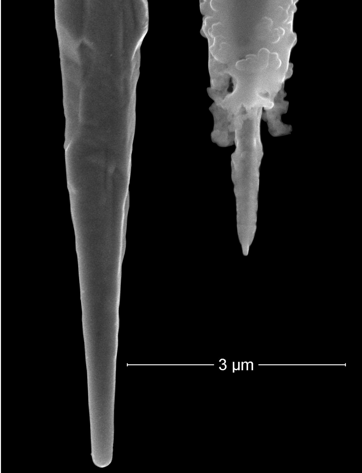
Comparative scanning electron microscope images of a freshly fabricated tungsten nanotip and a tip exposed to high field THz pulses are shown in Fig. 4, showing a strong reshaping of the apex of the tip. Over the course of several weeks of experiments, the tip length was reduced by approximately 3 m in length and the tip apex sharpened from a nm to nm radius. We note that over the course of an experiment in several hours to days, the emission rate was stable. Such field-induced sharpening of a nanotip has been previously observed in field-ion microscopy under applied dc bias voltage, and was used to produce single atom-terminated nanotips [37]. The mechanism for such dc field reshaping was determined to be the formation of tungsten nitride, causing a protrusion that in turn caused a local field enhancement. The local field then exceeded the evaporation threshold for the nitride and the atoms were removed. We therefore tentatively attribute the observed sharpening of the nanotip under intense THz fields to field evaporation of tungsten nitride on a shot-to-shot basis. However given the observed low energy electron distribution, we consider an alternative mechanism could be inelastic scattering of accelerated electrons within the nitride causing the removal of atoms in a similar manner. In this case, electrons transfer energy to regions with tungsten nitride, which are then selectively evaporated in the field thus sharpening the tip over time on a shot-to-shot basis.
In conclusion, we have demonstrated sub-cycle THz driven cold-field electron emission from a tungsten nanotip under extreme local field conditions. Electron bunch charges and peak current densities on the order of electrons/pulse and A/cm2 are quantitatively measured. Energies distribution up to 3.5 keV are observed and are accurately described by Fowler-Nordheim emission with ballistic acceleration in a quasi-static field. Seeing no signature of saturation in the emission current for increasing , combined with the field-induced sharpening of the nanotip and the predicted single-shot spectral purity of indicates that THz driven nanotip field emission holds promise for ultra-bright, ultrafast electron sources.
Acknowledgements
D. G. C. and B. J. S. gratefully acknowledge support from FRQNT, NSERC and the Canadian Foundation for Innovation (CFI). We thank Simon L. Lange and Prof. Peter Uhd Jepsen (Technical University of Denmark) for initial discussions and 3D simulations. We also thank Prof. Frank Hegmann (University of Alberta) for useful discussions.
References
- Krüger et al. [2018] M. Krüger, C. Lemell, G. Wachter, J. Burgdörfer, and P. Hommelhoff, Attosecond physics phenomena at nanometric tips, J. Phys. B-At. Mol. Opt. 51, 172001 (2018).
- Krüger et al. [2012] M. Krüger, M. Schenk, M. Förster, and P. Hommelhoff, Attosecond physics in photoemission from a metal nanotip, J. Phys. B-At. Mol. Opt. 45, 074006 (2012).
- Fowler and Nordheim [1928] R. H. Fowler and L. Nordheim, Electron emission in intense electric fields, P. R. Soc. Lond. A-Conta. 119, 173 (1928).
- Murphy and Good [1956] E. L. Murphy and R. H. Good, Thermionic emission, field emission, and the transition region, Phys. Rev. 102, 1464 (1956).
- Keldysh [1965] L. V. Keldysh, Ionization in the field of a strong electromagnetic wave, J. Exp. Theor. Phys+ 20, 1307 (1965).
- Wellershoff et al. [1999] S. S. Wellershoff, J. Hohlfeld, J. Güdde, and E. Matthias, The role of electron–phonon coupling in femtosecond laser damage of metals, Appl. Phys. A-Mater. 69, S99 (1999).
- Wimmer et al. [2014] L. Wimmer, G. Herink, D. R. Solli, S. V. Yalunin, K. E. Echternkamp, and C. Ropers, Terahertz control of nanotip photoemission, Nat. Phys. 10, 432 (2014).
- Herink et al. [2014] G. Herink, L. Wimmer, and C. Ropers, Field emission at terahertz frequencies: AC-tunneling and ultrafast carrier dynamics, New J. Phys. 16, 123005 (2014).
- Li and Jones [2016] S. Li and R. R. Jones, High-energy electron emission from metallic nano-tips driven by intense single-cycle terahertz pulses, Nat. Commun. 7 (2016).
- Echternkamp et al. [2016] K. E. Echternkamp, G. Herink, S. V. Yalunin, K. Rademann, S. Schafer, and C. Ropers, Strong-field photoemission in nanotip near-fields: from quiver to sub-cycle electron dynamics, Appl. Phys. B-Lasers O. 122, 80 (2016).
- Kilpatrick [1957] W. D. Kilpatrick, Criterion for vacuum sparking designed to include both rf and dc, Rev. Sci. Instrum. 28, 824 (1957).
- Wang and Loew [1989] J. W. Wang and G. A. Loew, RF breakdown studies in copper electron linac structures, in Proceedings of the 1989 IEEE Particle Accelerator Conference, . ’Accelerator Science and Technology (1989) pp. 1137–1139 vol.2.
- Herink et al. [2012] G. Herink, D. R. Solli, M. Gulde, and C. Ropers, Field-driven photoemission from nanostructures quenches the quiver motion, Nature 483, 190 (2012).
- Nanni et al. [2015] E. A. Nanni, W. R. Huang, K.-H. Hong, K. Ravi, A. Fallahi, G. Moriena, R. J. Dwayne Miller, and F. X. Kärtner, Terahertz-driven linear electron acceleration, Nat. Commun. 6, 8486 (2015).
- Rybka et al. [2016] T. Rybka, M. Ludwig, M. F. Schmalz, V. Knittel, D. Brida, and A. Leitenstorfer, Sub-cycle optical phase control of nanotunnelling in the single-electron regime, Nat. Photonics 10, 667 (2016).
- Ropers et al. [2007] C. Ropers, D. R. Solli, C. P. Schulz, C. Lienau, and T. Elsaesser, Localized multiphoton emission of femtosecond electron pulses from metal nanotips, Phys. Rev. Lett. 98, 043907 (2007).
- Quinonez et al. [2013] E. Quinonez, J. Handali, and B. Barwick, Femtosecond photoelectron point projection microscope, Rev. Sci. Instrum. 84, 103710 (2013).
- Daoud et al. [2017] H. Daoud, K. Floettmann, and R. J. Dwayne Miller, Compression of high-density 0.16 pC electron bunches through high field gradients for ultrafast single shot electron diffraction: The Compact RF Gun, Struct. Dynam.-US 4, 044016 (2017).
- Yeh et al. [2007] K.-L. Yeh, M. C. Hoffmann, J. Hebling, and K. A. Nelson, Generation of 10 ultrashort terahertz pulses by optical rectification, Appl. Phys. Lett. 90, 171121 (2007).
- Hirori et al. [2011] H. Hirori, A. Doi, F. Blanchard, and K. Tanaka, Single-cycle terahertz pulses with amplitudes exceeding 1 MV/cm generated by optical rectification in LiNbO3, Appl. Phys. Lett. 98, 091106 (2011).
- Lucier [2004] A. S. Lucier, Preparation and Characterization of Tungsten Tips Suitable for Molecular Electronics Studies, Ph.D. thesis, McGill University (2004).
- Yariv [1975] A. Yariv, Quantum Electronics (Wiley, John & Sons, 1975).
- Sinha and MacPhie [1977] B. P. Sinha and R. H. MacPhie, Electromagnetic scattering by prolate spheroids for plane waves with arbitrary polarization and angle of incidence, Radio Sci. 12, 171 (1977).
- [24] See Supplemental Material at [URL], which includes Refs. [8, 9, 35], for details on the transition between the quiver regime and the sub-cycle emission regime, the critical field and the three dimentional finite difference time domain simulations of the field enhancement at the nanotip.
- Forbes [2008] R. G. Forbes, Description of field emission current/voltage characteristics in terms of scaled barrier field values (-values), J. Vac. Sci. Technol. B: Microelectronics and Nanometer Structures Processing, Measurement, and Phenomena 26, 209 (2008).
- Forbes and Deane [2010] R. G. Forbes and J. H. B. Deane, Comparison of approximations for the principal Schottky–Nordheim barrier function , and comments on Fowler–Nordheim plots, J. Vac. Sci. Technol. B 28, C2A33 (2010).
- Bormann et al. [2010] R. Bormann, M. Gulde, A. Weismann, S. V. Yalunin, and C. Ropers, Tip-enhanced strong-field photoemission, Phys. Rev. Lett. 105, 147601 (2010).
- Yanagisawa et al. [2016] H. Yanagisawa, S. Schnepp, C. Hafner, M. Hengsberger, D. E. Kim, M. F. Kling, A. Landsman, L. Gallmann, and J. Osterwalder, Delayed electron emission in strong-field driven tunnelling from a metallic nanotip in the multi-electron regime, Sci. Rep.-UK 6, 35877 (2016).
- Tanuma et al. [2003] S. Tanuma, C. J. Powell, and D. R. Penn, Calculation of electron inelastic mean free paths (IMFPs) VII. Reliability of the TPP-2M IMFP predictive equation, Surf. Interface Anal. 35, 268 (2003).
- Wang and Mittleman [2004] K. Wang and D. M. Mittleman, Metal wires for terahertz wave guiding, Nature 432, 376 (2004).
- Wang and Mittleman [2005] K. Wang and D. M. Mittleman, Guided propagation of terahertz pulses on metal wires, J. Opt. Soc. Am. B 22, 2001 (2005).
- Soto et al. [2003] G. Soto, W. de la Cruz, F. Castillón, J. Díaz, R. Machorro, and M. Farías, Tungsten nitride films grown via pulsed laser deposition studied in situ by electron spectroscopies, Appl. Surf. Sci. 214, 58 (2003).
- Sun et al. [2004] Y.-M. Sun, E. Engbrecht, T. Bolom, C. Cilino, J. Sim, J. White, J. Ekerdt, and K. Pfeifer, Ultra thin tungsten nitride film growth on dielectric surfaces, Thin Solid Films 458, 251 (2004).
- Wicher et al. [2019] B. Wicher, R. Chodun, K. Nowakowska-Langier, M. Trzcinski, L. Skowroński, S. Okrasa, R. Minikayev, M. Naparty, and K. Zdunek, Chemical and structural characterization of tungsten nitride (WNx) thin films synthesized via Gas Injection Magnetron Sputtering technique, Vacuum 165, 266 (2019).
- Miller et al. [1996] M. K. Miller, A. Cerezo, M. Hetherington, and G. D. Smith, Atom probe field ion microscopy (Clarendon Press, 1996).
- Barbour et al. [1953] J. P. Barbour, W. W. Dolan, J. K. Trolan, E. E. Martin, and W. P. Dyke, Space-charge effects in field emission, Phys. Rev. 92, 45 (1953).
- Rezeq et al. [2006] M. Rezeq, J. Pitters, and R. Wolkow, Tungsten nanotip fabrication by spatially controlled field-assisted reaction with nitrogen, J. Chem. Phys. 124, 204716 (2006).