Ultra-fast amplitude modulation of mid-IR free-space beams at room-temperature
Abstract
Applications relying on mid-infrared radiation (Mid-IR, 3-30 ) have progressed at a very rapid pace in recent years, stimulated by scientific and technological breakthroughs. Mid-IR cameras have propelled the field of thermal imaging. And the invention of the quantum cascade laser (QCL) has been a milestone, making compact, semiconductor-based mid-IR lasers available to a vast range of applications. All the recent breakthrough advances stemmed from the development of a transformative technology. In addition to the generation and detection of light, a key functionality for most photonics systems is the electrical control of the amplitude and/or phase of an optical beam at ultra-fast rates (GHz or more). However, standalone, broadband, integrated modulators are missing from the toolbox of present mid-IR photonics integrated circuits and systems developers. We have developed a free-space amplitude modulator for mid-IR radiation ( 10 ) that can operate up to at least 1.5 GHz (-3dB cut-off at 750 MHz) and at room-temperature. The device relies on a semiconductor hetero-structure enclosed in a judiciously designed metal-metal optical resonator. At zero bias, it operates in the strong light-matter coupling regime up to 300K. By applying an appropriate bias, the device transitions to the weak coupling regime. The large change in reflectivity due to the disappearance of the polaritonic states is exploited to modulate the intensity of a mid-IR continuous-wave laser up to speeds of more than 1.5 GHz.
ModulatorMIR.bib]
Introduction
Fast amplitude and phase modulation are essential for a plethora of applications in mid-IR photonics, including laser amplitude/frequency stabilization [1], coherent detection, FM and AM spectroscopy and sensing, mode-locking, and optical communications [2, 3]. However, the ultra-fast (1-40 GHz) modulation of mid-IR radiation is a largely under-developed functionality. The fastest modulation speeds, 20-30 GHz, have been obtained with the direct modulation of mid-IR QCLs, but this requires specially designed devices and elevated injected RF (radiofrequency) powers [4, 5, 6]. Interestingly, in the visible/near-IR spectral ranges the preferred solution is to separate the functionalities: independent modulators, filters, interferometers are employed that are physically separated from the source. For modulators, this leads to advantages in terms of RF power, laser linewidth and flatness of the modulation bandwidth.
Commercially available mid-IR modulators are either acousto-optic devices with narrow modulation bandwidth, or very narrow band (100 kHz) electro-optic modulators based on GaAs or CdTe [7]. The latter ones can operate up to modulation speeds of 20 GHz, but their efficiency is very low (less than 0.1% sideband/carrier ratio). To date, standalone, efficient and broadband amplitude/phase modulators are missing from present mid-IR photonics tools.
One way forward is photonic integration: scaling to the mid-IR the approach already developed for silicon photonics. It can rely on SiGe/Si photonic platforms [8], or on the more natural InGaAs/AlInAs- on-InP platform [9]. In both cases the QCL source must be properly integrated in the system. An alternative is to develop modulators that can apply an ultra-fast RF modulation to a propagating beam, either in reflection or in transmission. This approach does not require a specific integration of the source and can in principle be applied to laser sources beyond QCLs.
In this letter we follow the latter strategy, and we demonstrate ultra-fast amplitude modulators of mid-IR free-space beams that operate at room-temperature in a reflection configuration (scheme in Figure 1(a)) up to more than 1 GHz modulation speed.
Since the eighties, proposals have been put forward to exploit intersubband (ISB) absorption in semiconductor quantum well (QW) systems to modulate mid-IR radiation. The first attempts based on the Stark shift were then followed by a number of works exploiting coupled QWs [10, 11]. In both cases, the application of an external bias depopulates the ground state of QW at 78K thus inducing a modulation of ISB absorption [12]. Operation at room temperature was obtained in [13] using a Schottky contact scheme. Recently, different approaches have been proposed to actively tune the reflectivity/transmission of mid-IR and/or THz beams: phase transition in materials like VO2 , liquid crystals orientation, carrier density control in metal-insulator-semiconductor junctions [14]. These devices operate on the principle that, at a given wavelength, a change in absorption translates in a modulation of the transmitted power. An alternative approach is to frequency shift the ISB absorption, instead of modulating its intensity. In [15, 16] a giant confined stark effect in a coupled QW system embedded in a metallic resonator, designed to be in the strong coupling regime between light and matter, was exploited. A response time of 10 ns was estimated.
Switching between strong and weak coupling regimes
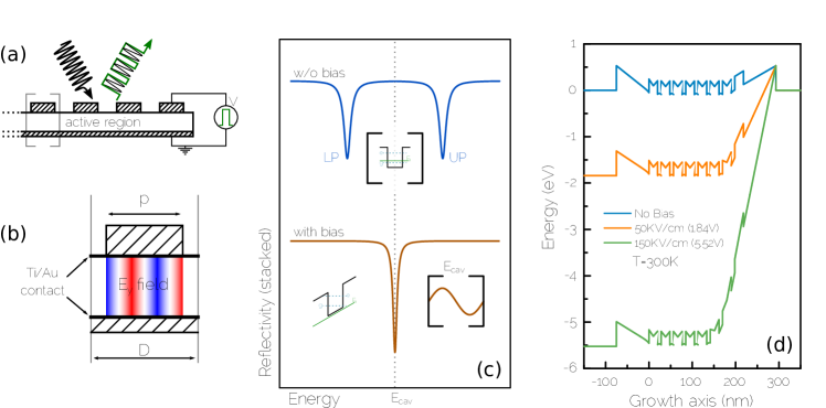
Our approach is to operate the device in the strong light-matter coupling regime, and introduce the ultra-fast modulation by switching the system in and out of strong coupling with the application of a bias voltage. A periodic QW structure is embedded in an optical resonator composed by non- dispersive metal-metal 1D ribbons (or 1D patch cavities [17]) as shown in Figure 1(a). The system, designed to operate in reflectance, is conveniently optimized so that the ISB transition is strongly coupled to the TM03 photonic mode of the resonator, whose electric-field distribution is shown in Figure 1(b). (The notation convention TM0i is defined in the caption). The resulting reflectivity R is sketched in Figure 1(c). At zero bias, at the cavity frequency for instance, R1 as the eigenmodes of the system are the upper (UP) and lower (LP) polaritons. An applied bias transitions the system, totally or partially, to the weak coupling regime, with a reflectivity drop down to R0. A laser with frequency (and so at and ) will be amplitude-modulated with an elevated contrast.
As the intersubband polariton dynamics features ps-level timescales [18], the bandwidth of the modulator is limited by (i) the RC-constant of the circuit and (ii) the transfer time of electrons in/out of the QWs. In fact, the top and bottom metal-semiconductor Schottky interfaces permit the application of a gate to the multiple QW structure that can efficiently deplete the system, as shown in Figure 1(d). Note: the electrical control of ISB polaritons, in a quasi-DC regime though, has been studied in [19, 20].
Sample fabrication
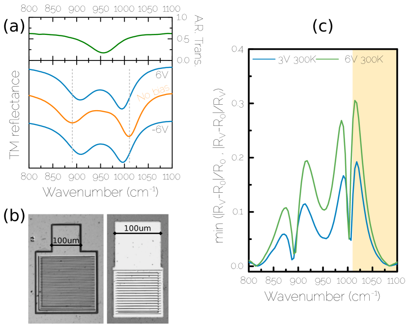
The semiconductor hetero-structure was grown by solid-source molecular beam epitaxy on an un- doped GaAs substrate. It is composed of 7 periods of 8.3 nm GaAs QWs separated by 20 nm-thick Al0.33Ga0.67As barriers. Si delta-doping () is introduced in the barrier center. A 40 nm-thick GaAs cap layer terminates the structure, and a 500 nm-thick Al0.50Ga0.50As is introduced before the active region, whose total thickness is LAR = 368.1 nm. The sample presents an ISB transition at an energy of 118.5 meV (about 955.8 ), that we have measured at 300K in a classic multipass waveguide transmission configuration (green spectrum in Figure 2(a) ). Figure 1(d) shows the global conduction band profile at room-temperature (RT, solid lines) and at different applied biases for the fabricated structure. It was obtained solving self-consistently the Schrodinger-Poisson equations using a commercial software [21]. With no applied bias all the QWs are populated. The application of a bias gradually depletes them.
The modulators rely on a metal-semiconductor-metal geometry. We have wafer-bonded the sample on a n+- GaAs carrier layer via Au-Au thermo-compression wafer-bonding, a standard technology for mid-IR polaritonic devices [22, 23]. After polishing and substrate removal, the 1D patches are defined with electron-beam lithography followed by Ti/Au deposition (5/80 nm) and lift-off. The top contact patterning and the definition of the bonding pads are realized with optical contact lithography and Ti/Au lift-off. An inductively coupled plasma (ICP) etching step down to the back metal plane defines the mesa structure. Optical microscope images of typical final devices are shown in Figure 2(b). Arrays of devices have been fabricated that differ in the width p of the metallic fingers (nomenclature in Figure 1(b)). For each value of p, we fabricated two arrays with different total surface ( and , respectively. Figure 2(b)). The active region being very thin (368.1 nm), the system does not operate as a photonic-crystal, but operates instead in the independent resonator regime. The cavity resonant frequency is set by p, not by the period D, according to the following expression:
The system behaves as a Fabry-Perot cavity of length p, with n an effective index that takes into account the reflectivity phase at the metallic boundaries [17, 24]. We opted to operate not on the i=1 fundamental mode, the standard choice [17], but on the i=3 mode (the TM03), to simplify the fabrication procedure and increase the electromagnetic overlap factor. Figures S1 and S2 in Supplementary Material provides a justification for this choice.
Experimental results
The reflectance of the devices as a function of p has been measured with a microscope coupled to an FTIR spectrometer to retrieve the polaritonic positions at RT (and at 78K) with no applied bias. The complete dispersion is shown in Figure S2 : together with the measurements and simulations on an empty cavity (Figure S1) it permits to identify the first 3 ribbon resonator modes. The TM03 mode exhibits a clear Rabi splitting for patch sizes around p = 4 .
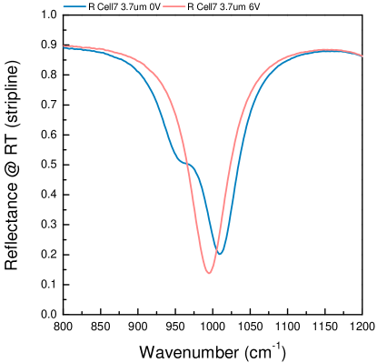
A suitable device (p = 4.2 ) was wire bonded and its reflectance was measured under different applied DC biases. When no bias is applied, we observe (orange curve in Figure 2(a)) the 2 polariton branches. The two blue solid lines correspond to a 6V applied bias, that is practically the limit imposed by the Ti/Au Schottky barriers. The Rabi decreases by 25%: it means that the gate empties only half of the QWs, as , being N the total number of QWs in the structure. (A different, lower doped sample that fully transitions to the weak coupling regime is reported in Figure S3 of Suppl. Material).
From the measurements we can extract the modulation depth attainable on an incoming laser beam with a +6V maximum bias with this specific device. The modulation is defined as and it is plotted in Figure 2(c) in the 800 - 1100 range. It shows that a contrast above 10% can be obtained in a few frequency ranges. In particular, a contrast between 20% and 30% can be obtained around 1030 ( 9.70 ). This frequency is covered by our tunable commercial QC laser (shadowed orange region in Figure 2(c)).
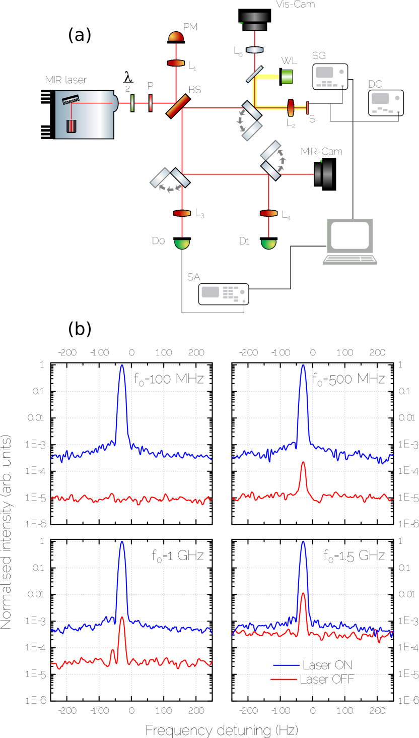
We have measured the speed and modulation bandwidth of the modulator with the setup described in Figure 3(a). A continuous-wave (CW), tunable commercial QC laser [25] is focused on the modulator (S) that is fed with an RF signal from a synthesizer (SG). The reflected, and modulated, beam is detected with a 837 MHz-bandwidth commercial MCT detector (D0, [26]) whose output is fed to a spectrum analyzer (SA), or – for low frequency measurements – to a 50 MHz-bandwidht MCT detector (D1) and then to a 200 MHz lock-in amplifier. All measurements are performed at room temperature (300K).
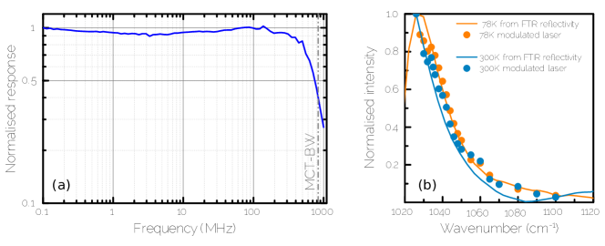
Figure 3(b) shows the spectra obtained from the smaller modulator (p=4.1 ), using a QCL frequency of 1010 . We can detect a signal up to a modulation speed of 1.5 GHz, well beyond the VIGO detector 3dB cutoff of 837 MHz, proving the ultra-fast character of our modulator. In order to determine the modulator bandwidth, we performed an automated scan as a function of the modulation frequency. The results, at 300K, are reported in Figure 4(a) for a typical 100x100 2 large device, with grating period p=4.1 . At the optimum performance point ( = 1010 ), it operates at frequencies > 1GHz, with a -3dB cut-off at 750 MHz (Figure 4(a), blue curve). The larger devices (data not shown) typically exhibit a -3dB cut-off at 150 MHz. This result is in fair agreement with the surface ratio between the two devices. Furthermore the theoretical RC-cutoff of the large samples is 204MHz and for the small sample 510MHz (C device capacitance and R the 50 output resistance of the RF syntesizer). The good agreement proves that the bandwidth is currently limited by the RC time constant. For high-resolution spectroscopy, an important parameter is the sideband/carrier power ratio. For the current modulators, we estimate a ratio of the order of 5%.
If the QC laser frequency is tuned away from the optimum value, Figure 2(c) predicts that the modulation contrast should drop. This observation is crucial to unambiguously assign to the polariton modulation the enabling physical principle of the device. To this scope we have measured the modulation contrast as a function of the QCL laser frequency, at both RT and 78K. The results – normalized to 1 - are reported in Figure 4(b) (dots) for the larger sample, and they are superimposed to the DC modulation response curve obtained from the reflectivity measurements from 2(c). The modulator ultra-fast response as a function of the impinging laser frequency closely follows the DC contrast curve. This finding confirms that the enabling mechanism is indeed the ultra-fast modulation of the Rabi splitting via application of an RF signal.
Discussion and conclusions
Having established that the current devices are RC limited, the natural question is: what is their intrinsic speed? The physics of the current devices is not very different from the one of mid-IR QWIP detectors, except the absence of the ohmic contacts, that are known to operate up to speeds of 60/80 GHz [28, 29]. That alone suggests that the intrinsic speed of the current modulators is set by the same parameters, in particular the capture time and the transit time that is set by the drift velocity. There is however a notable difference: in the ideal operating regime, carriers diffuse all the way towards one metal-semiconductor interface upon application of a bias. And they have to flow back through the active region when the bias is restored to 0. This leads of a characteristic time . In our case, with a very conservative at RT [30], we obtain a value of ps which sets a lower bound for the intrinsic cut-off at < 10 GHz.
In conclusion, we have demonstrated a technology that is able to amplitude modulate mid-IR free space laser beams up to GHz modulation frequencies. In this first demonstration, at = 9.7 , we achieved modulation speeds up to 1.5 GHz at room temperature (-3dB cut-off at 750 MHz). The device operates by transitioning in and out of the strong coupling regime at ultra-fast rates, and it is possibly the first report of a practical device relying on the strong light-matter coupling regime. The estimated intrinsic speed is at minimum 10 GHz. Improved active regions that do not rely on drift transport, but instead on tunnel coupling [20] will probably lead to modulation speed in the 30/40 GHz range.
Funding Information
We acknowledge financial support from the European Union FET-Open Grant MIRBOSE (737017). This work was partly supported by the French RENATECH network. R.C. and A.B. acknowledge financial support from the French National Research Agency (project “IRENA”).
Acknowledgments
We thank S. Barbieri, J-F. Lampin and E. Peytavit for useful discussions. We also thank L. Wojszvzyk, A.
Nguyen and J-J. Greffet for the loan of the 50 MHz-bandwidth MCT detector.
Disclosures. The authors declare no conflicts of interest.
See Supplementary material below for supporting content.
References
- [1] V. Bernard, Ch. Daussy, G. Nogues, L. Constantin, P.E. Durand, A. Amy-Klein, A. Van Lerberghe and Ch. Chardonnet “CO2 laser stabilization to 0.1-Hz level using external electrooptic modulation” In IEEE Journal of Quantum Electronics 33.8 IEEE, 1997, pp. 1282–1287
- [2] R. Martini, R. Paiella, C. Gmachl, F. Capasso, E.A. Whittaker, H.C. Liu, H.Y. Hwang, D.L. Sivco, J.N. Baillargeon and A.Y. Cho “High-speed digital data transmission using mid-infrared quantum cascade lasers” In Electronics Letters 37.21 IET, 2001, pp. 1290–1292
- [3] Liu Chuanwei, Zhai Shenqiang, Zhang Jinchuan, Zhou Yuhong, Jia Zhiwei, Liu Fengqi and Wang Zhanguo “Free-space communication based on quantum cascade laser” In Journal of Semiconductors 36.9 IOP Publishing, 2015, pp. 094009
- [4] Roberto Paiella, Rainer Martini, Federico Capasso, Claire Gmachl, Harold Y. Hwang, Deborah L. Sivco, James N. Baillargeon, Alfred Y. Cho, Edward A. Whittaker and H.C. Liu “High-frequency modulation without the relaxation oscillation resonance in quantum cascade lasers” In Applied Physics Letters 79.16 American Institute of Physics, 2001, pp. 2526–2528
- [5] Borislav Hinkov, Jakob Hayden, Rolf Szedlak, Pedro Martin-Mateos, Borja Jerez, Pablo Acedo, Gottfried Strasser and Bernhard Lendl “High frequency modulation and (quasi) single-sideband emission of mid-infrared ring and ridge quantum cascade lasers” In Optics Express 27.10 Optical Society of America, 2019, pp. 14716–14724
- [6] A. Mottaghizadeh, Z. Asghari, M. Amanti, D. Gacemi, A. Vasanelli and C. Sirtori “Ultra-Fast modulation of mid infrared buried heterostructure quantum cascade lasers” In 2017 42nd International Conference on Infrared, Millimeter, and Terahertz Waves (IRMMW-THz), 2017, pp. 1–2 IEEE DOI: 10.1109/irmmw-thz.2017.8067122
- [7] QUBIG GmbH, https://www.qubig.com/
- [8] Vladyslav Vakarin, Joan Manel Ramírez, Jacopo Frigerio, Andrea Ballabio, Xavier Le Roux, Qiankun Liu, David Bouville, Laurent Vivien, Giovanni Isella and Delphine Marris-Morini “Ultra-wideband Ge-rich silicon germanium integrated Mach–Zehnder interferometer for mid-infrared spectroscopy” In Optics Letters 42.17 Optical Society of America, 2017, pp. 3482–3485
- [9] Seungyong Jung, Daniele Palaferri, Kevin Zhang, Feng Xie, Yae Okuno, Christopher Pinzone, Kevin Lascola and Mikhail A Belkin “Homogeneous photonic integration of mid-infrared quantum cascade lasers with low-loss passive waveguides on an InP platform” In Optica 6.8 Optical Society of America, 2019, pp. 1023–1030
- [10] N. Vodjdani, B. Vinter, V. Berger, E. Böckenhoff and E. Costard “Tunneling assisted modulation of the intersubband absorption in double quantum wells” In Applied physics letters 59.5 American Institute of Physics, 1991, pp. 555–557
- [11] E. Dupont, D. Delacourt, V. Berger, N. Vodjdani and M. Papuchon “Phase and amplitude modulation based on intersubband transitions in electron transfer double quantum wells” In Applied Physics Letters 62.16, 1993, pp. 1907–1909 DOI: 10.1063/1.109539
- [12] J.. Duboz, V. Berger, N. Laurent, D. Adam and J. Nagle “Grating coupled infrared modulator at normal incidence based on intersubband transitions” In Applied Physics Letters 70.12, 1997, pp. 1569–1571 DOI: 10.1063/1.118619
- [13] V. Berger, N. Vodjdani, D. Delacourt and J.. Schnell “Room-temperature quantum well infrared modulator using a Schottky diode” In Applied Physics Letters 68.14, 1996, pp. 1904–1906 DOI: 10.1063/1.116289
- [14] Young Chul Jun, Edward Gonzales, John L. Reno, Eric A. Shaner, Alon Gabbay and Igal Brener “Active tuning of mid-infrared metamaterials by electrical control of carrier densities” In Optics Express 20.2 OSA, 2012, pp. 1903–1911 DOI: 10.1364/OE.20.001903
- [15] Alexander Benz, Inès Montaño, John F. Klem and Igal Brener “Tunable metamaterials based on voltage controlled strong coupling” In Applied Physics Letters 103.26, 2013, pp. 263116 DOI: 10.1063/1.4859636
- [16] Jongwon Lee, Seungyong Jung, Pai-Yen Chen, Feng Lu, Frederic Demmerle, Gerhard Boehm, Markus-Christian Amann, Andrea Alù and Mikhail A. Belkin “Ultrafast Electrically Tunable Polaritonic Metasurfaces” In Advanced Optical Materials 2.11, 2014, pp. 1057–1063 DOI: 10.1002/adom.201400185
- [17] Yanko Todorov, Lorenzo Tosetto, Jean Teissier, Aaron Maxwell Andrews, Pavel Klang, Raffaele Colombelli, Isabelle Sagnes, Gottfried Strasser and Carlo Sirtori “Optical properties of metal-dielectric-metal microcavities in the THz frequency range” In Optics Express 18.13 Optical Society of America, 2010, pp. 13886–13907
- [18] G. Günter, Aji A. Anappara, J. Hees, Alexander Sell, Giorgio Biasiol, Lucia Sorba, S. De Liberato, Cristiano Ciuti, Alessandro Tredicucci, Alfred Leitenstorfer and R. Hubert “Sub-cycle switch-on of ultrastrong light–matter interaction” In Nature 458.7235 Nature Publishing Group, 2009, pp. 178–181
- [19] Aji A Anappara, Alessandro Tredicucci, Giorgio Biasiol and Lucia Sorba “Electrical control of polariton coupling in intersubband microcavities” In Applied Physics Letters 87.5 American Institute of Physics, 2005, pp. 051105
- [20] Aji A. Anappara, Alessandro Tredicucci, Fabio Beltram, Giorgio Biasiol and Lucia Sorba “Tunnel-assisted manipulation of intersubband polaritons in asymmetric coupled quantum wells” In Applied Physics Letters 89.17, 2006, pp. 171109 DOI: 10.1063/1.2367664
- [21] Stefan Birner, Tobias Zibold, Till Andlauer, Tillmann Kubis, Matthias Sabathil, Alex Trellakis and Peter Vogl “Nextnano: general purpose 3-D simulations” In IEEE Transactions on Electron Devices 54.9 IEEE, 2007, pp. 2137–2142
- [22] Pierre-Baptiste Vigneron, Stefano Pirotta, Iacopo Carusotto, Ngoc-Linh Tran, Giorgio Biasiol, Jean-Michel Manceau, Adel Bousseksou and Raffaele Colombelli “Quantum well infrared photo-detectors operating in the strong light-matter coupling regime” In Applied Physics Letters 114.13 AIP Publishing LLC, 2019, pp. 131104
- [23] J-M. Manceau, N-L Tran, G. Biasiol, T. Laurent, I. Sagnes, G. Beaudoin, S. De Liberato, I. Carusotto and R. Colombelli “Resonant intersubband polariton-LO phonon scattering in an optically pumped polaritonic device” In Applied Physics Letters 112.19 AIP Publishing LLC, 2018, pp. 191106
- [24] Matthieu Duperron “Conception et caractérisation de nanoantennes plasmoniques pour la photodétection infrarouge refroidie”, 2013
- [25] DRS Daylight Solutions, https://www.daylightsolutions.com/
- [26] VIGO System, https://vigo.com.pl/en/home/
- [27] , https://pymeasure.readthedocs.io/en/latest/
- [28] Hui C. Harald Schneider “Quantum Well Infrared Photodetectors - Physics and Applications” Springer-Verlag Berlin Heidelberg, 2007
- [29] Q. Lin, M Hakl, S Pirotta, R. Colombelli, W. Wan, H Li, J. Cao, J-F Lampin, E. Peytavit and S Barbieri “Development of high-speed, patch-antenna intersubband photodetectors at 10.3um” Poster, 44th International Conference on Infrared, Millimeter, and Terahertz Waves, IRMMW-THz 2019, 2019 URL: https://hal.archives-ouvertes.fr/hal-02323396
- [30] S. Hava and M. Auslender “Velocity-field relation in GaAlAs versus alloy composition” In Journal of Applied Physics 73.11 American Institute of Physics, 1993, pp. 7431–7434
References
- [31] “Handbook of optical constants of solids” Academic press, 1998
- [32] Constantine A Balanis “Antenna theory: analysis and design” John wiley & sons, 2016
ModulatorMIR_supp.bib] \appendixpage
Bare cavity reflectivity
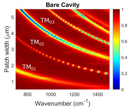
Rigorous Coupled Wave Analysis (RCWA) simulation for a 1D metallic ribbon bare cavity, as schematized in Fig. 1(a) of the main paper. The thickness of the insulator layer (GaAs) is 368.1 nm. The effective dielectric function of GaAs taking into account the interaction with phonons is in the following form:
where is the relative permittivity at high frequency, the damping of the phonon mode, = 292 and = 268 are the longitudinal optical phonon and transverse optical phonon frequencies, respectively [31].
The metal strip size (patch width, p in the main text) varies from 0.5 to 5.5 . The distance between the metal ribbons is kept constant at 1.5 .
Polarized light, with the electric field orthogonal to the metal ribbons, is directed onto the surface and the reflectivity is simulated for each width at the incident angle of 10 degree. For this reason the mode TM02, which is non-radiative at normal incidence, is only barely visible. Mode TM03 is the one with the largest contrast [32].
Sample HM4099 reflectivity
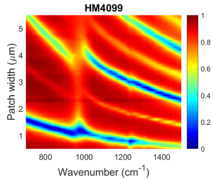
Experimental reflectivity measurement of the doped sample HM4099 at 300 K. The sample was nominally doped to a sheet concentration of . The bare intersubband transition is measured at 955.8 .
The top metallic grating was implemented by electron beam lithography. The ribbons width varies from 0.5 to 5.5 and the distance between the metal stripes is 1.5 .
The reflectivity measurements were performed with a Nicolet FTIR microscope with polarized light light, resolution of 8 , using a liquid nitrogen cooled MCT detector. The Rabi splitting is clearly observed for the TM03 mode, presenting evidence of strong light-matter coupling between the cavity mode and the intersubband transition.
The modulator devices have been designed based on these measurements, in order to operate on the TM03 mode.
Reflectance at 300K of sample HM4098 (N)
We present here data on sample HM4098, that is a lower doped sample. The nominal sheet doping per QW is (N).
In this case the application of a bias completely transitions the system from the strong coupling into the weak coupling regime. However, the reduced Rabi splitting with respect to sample HM4099 yields a lower reflectivity contrast when implemented as a modulator. For this reason, we have employed sample HM4099 to implement modulators.