figurec \alsoaffiliationSchool of Physics, The University of Melbourne, Parkville, 3010, Victoria, Australia.
Tunable band-gap and isotropic light absorption from bismuth-containing GaAs coreshell and multishell nanowires
Abstract
Semiconductor coreshell nanowires based on the GaAs substrate are building blocks of many photonic, photovoltaic and electronic devices, thanks to the associated direct band-gap and the highly tunable optoelectronic properties. The selection of a suitable material system is crucial for custom designed nanowires tailored for optimised device performance. The bismuth containing GaAs materials are an imminent class of semiconductors which not only enable an exquisite control over the alloy strain and electronic structure but also offer the possibility to suppress internal loss mechanisms in photonic devices. Whilst the experimental efforts to incorporate GaBixAs1-x alloys in the nanowire active region are still in primitive stage, the theoretical understanding of the optoelectronic properties of such nanowires is only rudimentary. This work elucidates and quantifies the role of nanowire physical attributes such as its geometry parameters and bismuth incorporation in designing light absorption wavelength and polarisation response. Based on multi-million atom tight-binding simulations of the GaBixAs1-x/GaAs coreshell and GaAs/GaBixAs1-x/GaAs multishell nanowires, our results predict a large tuning of the absorption wavelength, ranging from 0.9 m to 1.6 m, which can be controlled by engineering either Bi composition or nanowire diameter. The analysis of the strain profiles indicates a tensile character leading to significant light-hole mixing in the valence band states. This offers a possibility to achieve polarisation-insensitive light interaction, which is desirable for several photonic devices involving amplification and modulation of light. Furthermore, at low Bi compositions, the carrier confinement is quasi type-II, which further broadens the suitability of these nanowires for myriad applications demanding large carrier separations. The presented results provide a systematic and comprehensive understanding of the GaBixAs1-x nanowire properties and highlight new possibilities for future technologies in photonics, quantum optics and solar energy harvesting.
keywords:
Nanowire, Photonics Devices, Strain, Optical Transitions, Charge ConfinementsSemiconductor nanowires are versatile nanostructures which provide access to a unique set of electronic and optical characteristics suitable for many photonic applications 1, 2. The recent advancements in the growth techniques have allowed an exquisite control of nanowire morphologies, leading to engineered properties tailored for device functionalities. This has opened up tremendous opportunities for application of nanowires in the realization of a wide range of high-performance optoelectronic devices, including solar cells, photodetectors, light sensors, optical modulators, optical amplifiers and solid-state light sources 3, 4, 5, 6, 7, 8. More recently, there are proposals for novel applications of nanowires in cross-disciplinary fields such as medical imaging and solar to fuel conversion. Consequently, in the last few years, semiconductor nanowires have been a topic of major research efforts on both experimental and theoretical fronts, where the focus has been to optimise nanowire parameters such as its geometry dimensions and composition to enable directed applications in next generation technologies.
For nanowire growth and design, a large number of material systems have been investigated in the literature including III-Vs (such as GaAs, GaNAs, InGaP, GaPAs) 3, 4, 5, 6, 7, 8, SiGe 9, and ZnO 10, among several others. The nanowires made up of GaAs based III-V materials have been of particular interest due to highly promising optoelectronic characteristics, possibilities of dislocation free epitaxial growth, and monolithic integration with a large number of substrates including technologically relevant silicon 4, 11 and graphene 12. One particular class of nanowires is known as coreshell nanowires, where the core and shell regions are made up of different III-V materials such as GaAs and InGaAs 13. There has also been studies for designing nanowires with multishell structures where each shell is grown with a different alloy composition to allow engineered carrier confinement and light interactions 14. The coreshell nanowires have been shown to offer excellent tuning of optoelectronic properties because the strain and electronic confinement can be controlled by designing the size of the core and shell regions as well as the alloy compositions.
The nanowires formed by the conventional GaAs alloy materials such as InGaAs, InGaP, and AlGaAs have been around for many years and their optoelectronic properties are well studied in the literature 15, 16, 17, 18, 11. However, very recently, the focus has been shifted towards incorporating highly-mismatched bismuth containing GaAs materials such as GaBixAs1-x in the active region of coreshell nanowires 19, 20, 21, 22, 23, 24, 25, 26. The GaBixAs1-x materials which are formed by adding dilute concentration of bismuth (Bi) in the GaAs material offer unique electronic properties which are not readily accessible from traditional III-V alloys. It has been shown that the band-gap energy of the GaBixAs1-x material decreases dramatically with increasing Bi composition 27, 28, 29, 30, 31, 32. This implies that the band-gap energy can be tuned to a wide spectral range, encompassing near, mid and far infra-red bands (1-10 m). The spectroscopic ellipsometry study has shown that the refractive index for the GaBixAs1-x material increases with Bi fraction and is slightly larger than that of the GaAs material 33. Another highly promising property of the GaBixAs1-x material system originates from very large spin-orbit coupling associated with the GaBi material (2.3 eV), which leads to a spin-orbit splitting energy being greater than the band-gap energy in the telecommunication spectral range (1550 nm) a property which is not available from other GaAs based materials. The spin-orbit splitting energy larger than the band-gap energy is highly desirable for the suppression of internal loss mechanisms such as inter-valence band absorption (IVBA) and CHSH Auger recombination processes which plague the efficiency of many photonic devices 34, 29, 35, 36, 37. Therefore, a systematic and comprehensive understanding of the GaBixAs1-x coreshell and multishell nanowires such as presented in this work is expected to play an important role towards exploiting the unique characteristics of this imminent material system for the next generation photonic devices.
The interest in the GaBixAs1-x nanowires is at its primitive stage and the first few experimental studies have been reported in the literature during the last three to four years 19, 20, 21, 22, 23, 24, 25, 26. Theoretically, GaBixAs1-x coreshell and multishell nanowires have not been studied in much detail. Recently, GaBixAs1-x/GaAs nanowires were theoretically investigated where the core region was made up of the GaBixAs1-x material surrounded by a GaAs shell region 38. Here, in this work the focus is on GaBixAs1-x nanowires where the core region is made up of GaAs region and the GaBixAs1-x alloys is present in the shell region. Such nanowires are highly relevant to many experimental studies on the III-V coreshell nanowires where a tertiary or quaternary alloy is typically present in the shell region and the core region is a binary material. As the experimental research on GaBixAs1-x nanowires is rapidly advancing, there are several open questions regarding incorporation of Bi in the nanowire active region, such as the band-gap dependence on the Bi fraction, the charge carrier confinements and the sensitivity to the light polarisation. The answers to these questions are crucial to target nanowire parameters tailored for photonic applications. This work aims to provide a timely guidance for future experiments and will contribute significantly in the advancement of an emerging area of research.
This work is based on the state-of-the-art atomistic tight-binding simulations, which have been carried out on 4 to 8 million atoms to understand the optoelectronic properties of GaBixAs1-x nanowires with realistic geometry parameters. The accuracy of the tight-binding model was verified against the available experimental data sets in a number published studies including on band-gap variation of the GaBixAs1-x bulk material as a function of Bi composition with 39 and without 29 strain, and GaBiAs/GaAs quantum well structures 40. Subsequent studies based on DFT model 41, 42, 43 and experimental measurements 44, 45, 46, 47, 48, 29, 39, 49 demonstrated a good agreement with the simulated results, which again affirmed the high-level accuracy of our atomistic techniques. We also note that in contrast to the simplified models used in the literature such band anti-crossing method, effective-mass and models 37, 50, 50, 51 which have been quite successful to qualitatively model GaBixAs1-x based photonic devices, the atomistic tight-binding simulations employed here explicitly represent the nanowire geometries with atomic resolution. This allows to incorporate the impact of additional effects such as alloy randomness and interface roughness, which have been shown to play an important role in the investigation of electronic and optical properties of GaBixAs1-x materials 39, 52 and more generally for several other nanostructures 53, 54. Therefore, this work is expected to provide a highly reliable quantitative understanding of the optoelectronic properties of the investigated GaBixAs1-x coreshell nanowires, which will be directly relevant to the ongoing experimental efforts.
The reported results have uncovered novel properties of the GaBixAs1-x/GaAs nanowires which further motivates interest in this material system and highlight opportunities for a wide range of applications. We show that the inter-band absorption wavelength is highly sensitive to the nanowire diameter and Bi fraction of the shell region, and can be tuned from 0.9 m to 1.6 m. This provides a two-way knob to control light absorption/emission energies. Another interesting property of the GaBixAs1-x/GaAs nanowires reported in this work is the transition from quasi type-II carrier confinement to type-I carrier confinement, which occurs at low Bi fractions (3%). This property is useful for designing a variety of devices where large carrier separation or strong light absorption is the parameter of interest. Finally, our results demonstrate that the GaBixAs1-x/GaAs nanowires provide a strong light-hole absorption, which couples to TM polarisation mode. This is in contrast to usual III-V nanostructures where typically TE mode absorption is dominant. We also show the possibility of isotropic light polarisation at 1.55 m wavelength which is important for many optical devices such as semiconductor optical amplifiers and modulators. Overall, our results indicate that GaBixAs1-x/GaAs nanowires can be custom designed to target desired properties and hence are expected to find myriad applications in nanophotonic and nanoelectronic technologies.
Results and Discussions
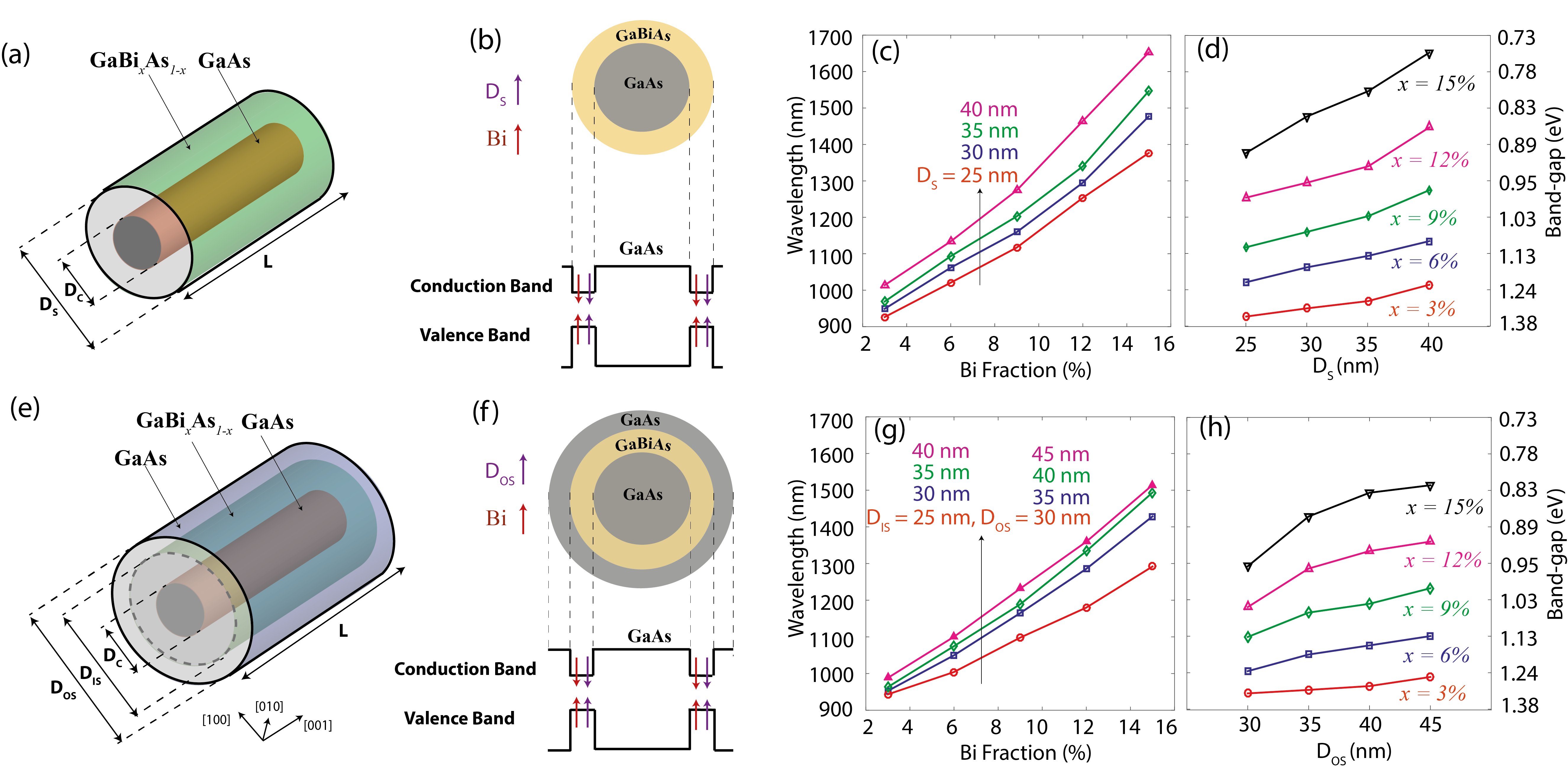
In this work, we have investigated two types of coreshell nanowires as shown by the schematic diagrams in Figure 1. Both types of nanowire consist of a GaAs core region with a core diameter () of 20 nm. The GaBixAs1-x/GaAs nanowire in Figure 1 (a) has a single outer shell made up of GaBixAs1-x material with a shell diameter () varying from 25 nm to 40 nm. The Bi composition of the shell region is varied from 3% to 15%. The second type of nanowire GaAs/GaBixAs1-x/GaAs studied in this work consists of two shell regions: an inner shell made up of GaBixAs1-x material with diameter and an outer shell made up of GaAs material with diameter . Such nanowire structures are also referred to as quantum well nanowires in the literature 55 and provide an extra degree of freedom to engineer nanowire properties. The diameter is varied from 25 nm to 40 nm as for the previous case of GaBixAs1-x/GaAs nanowires. The thickness of the outer shell in all cases is selected as 5 nm, therefore varies from 30 nm to 45 nm. The nanowires are constructed atomistically, where the GaBixAs1-x shell region contains Bi atoms randomly replacing As atoms. The length of nanowires is selected as 80 nm, however the previous study has shown that the electronic band-gap energy is relatively independent of the nanowire length. The largest dimension of the GaBixAs1-x/GaAs and GaAs/GaBixAs1-x/GaAs nanowires consists of roughly 6.3 million and 8 million atoms respectively, in the simulation domain. The number of Bi atoms in the active region for 15% Bi composition are around 0.47 million. The nanowires structures are relaxed by valence force field (VFF) model and the internal strain is computed from the relaxed atom positions. The electronic structure is computed by solving a ten-band sp3s∗ tight-binding Hamiltonian which explicitly includes spin-orbit coupling. The lowest electron and the highest hole energies are computed at the point. Further details of the methods are provided in the Methods section.
Band-gap Tuning
Figure 1 (a) shows the schematic diagram of the studied GaBixAs1-x/GaAs coreshell nanowires. The band-gap energy of the nanowire is investigated by varying two parameters: the Bi fraction () in the GaBixAs1-x shell region and the diameter () of the shell region. The changes in the conduction and valence band edges are schematically indicated in Figure 1 (b) when and are increased. The increase in the Bi fraction reduces the conduction band edge energy and increases the valence band edge energy, in agreement with the previous studies on GaBixAs1-x bulk and quantum well systems 29, 39, 40. We find the same trend when the shell diameter of the nanowire is increased. Consequently, the band-gap energy decreases as a function of both Bi fraction and shell diameter. The band-gap dependence on the Bi fraction is plotted in Figure 1 (c) for various shell diameters. Our calculations show that by increasing the Bi fraction from 3% to 15%, the band-gap energy can be tuned from 1.38 eV to 0.78 eV (corresponding to a change of 900 nm to 1600 nm in the optical absorption wavelength). Likewise, a reduction in the band-gap energy is computed with an increase in shell diameter, which is stronger at larger Bi compositions. We compute a red shift of about 36 meV and 40 meV per % increase in the Bi fraction at = 25 nm and 40 nm, respectively. Figure 1 (d) shows the dependence of the band-gap energy on the nanowire shell diameter when the Bi faction is kept constant. The decrease(increase) in the band-gap energy(wavelength) is stronger at 15% Bi fraction when compared to the 3% Bi composition. Overall, we find that the band-gap energy is highly sensitive to both Bi composition and the nanowire diameter, and can be tuned in the telecommunication spectra.
In experimental studies, often multishell nanowires, also known as quantum well nanowires, are investigated where the nanowires are made up of two or more shell regions. In such nanowires, for example the outer shell and core regions can be made up of the same material composition whereas the inner shell designed with an alloy forming the active region of the nanowire for charge carrier confinements and/or transport. In this work, we also investigate the effect of GaAs outer shell forming GaAs/GaBixAs1-x/GaAs nanowires as shown in Figure 1 (e). The band edge changes for such nanowires are schematically illustrated in Figure 1 (f), where the core and outer shell regions correspond to the larger band-gap GaAs material and the inner shell region is small band-gap GaBixAs1-x material which provides carrier confinement. The dependence of the band-gap energy (optical wavelength) on the Bi fraction inside the inner shell region is shown in Figure 1 (g), which exhibits a very similar trend as reported above for the GaBixAs1-x/GaAs nanowires. We calculate approximately 29 meV and 36 meV reductions in the band-gap energies per % Bi increase for = 25 nm and 40 nm, respectively. These changes are slightly smaller than computed for the GaBixAs1-x/GaAs nanowires reported above. We also note that the reduction in the band-gap energy per % increase in Bi composition for the investigated nanowires is significantly lower than the previously computed 90 meV reduction per % Bi increase for the bulk GaBixAs1-x alloy. This can be attributed to the fact that for bulk GaBixAs1-x alloys, the incorporation of Bi strongly effect the band edge energies, in particular the valence band edge energy due to the band anti-crossing effect. However, for nanostrucures such as nanowires this band anti-crossing effect is modulated by other factors such as quantum confinement and internal strain which all contributes to the net reduction of the band-gap energy.
Figure 1 (h) plots the dependence of the band-gap energy (optical transition wavelength) for GaAs/GaBixAs1-x/GaAs nanowires as a function of nanowire diameter by keeping the Bi fraction constant in the inner shell region. Interestingly, we compute a strong impact of the GaAs outer shell on the band-gap energy reduction when compared to the GaBixAs1-x/GaAs nanowires. The band-gap energy decreases as a function of the diameter but the rate of decrease is noticeably slower. In particular, the band-gap energy becomes relatively flat at higher Bi fractions (12% and 15%). This implies that for GaAs/GaBixAs1-x/GaAs nanowires, the increase in the nanowire diameter will only negligibly shift the band-gap energy for Bi fractions above 12%. This non-trivial behaviour of nanowire band-gap reduction is a direct consequence of the internal strain modulation by the GaAs outer shell region, which will be discussed in the next strain analysis section.
We want to conclude this section by summarising that a large tunable band-gap energy (optical transition wavelength) is accessible from the investiagted GaBixAs1-x/GaAs and GaAs/GaBixAs1-x/GaAs nanowires, which can be controlled by engineering geometry parameters (i.e. nanowire diameters and/or Bi fractions). Importantly, we find that for Bi fractions around 15%, the optical transition wavelength is in the spectral range of interest for telecommunication devices (1550 nm) which will be desirable for a variety of photonic devices.
Strain Analysis
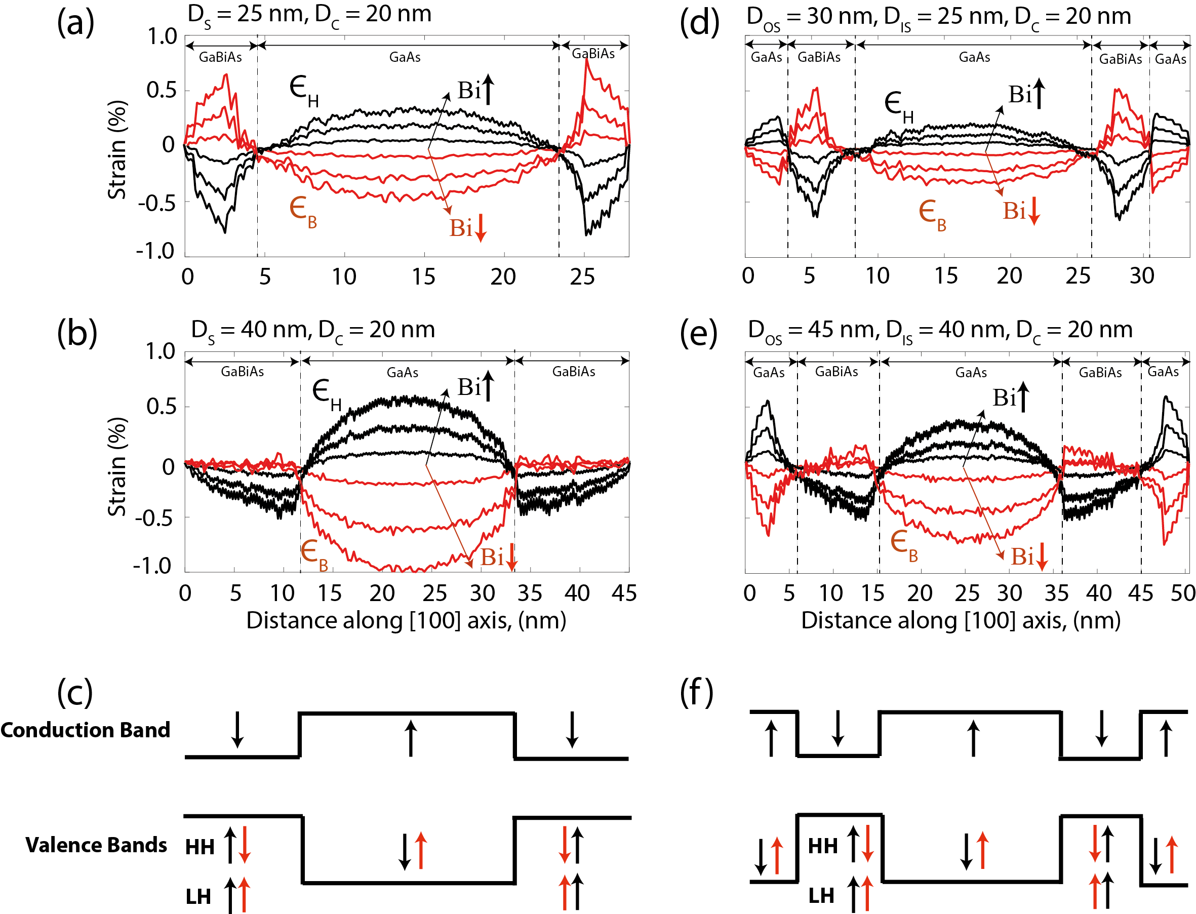
In order to understand the band-gap energy shifts discussed in the previous section, it is imperative to analyse strain profiles which directly affect the electron and hole energies and wave functions 56. The nanowires studied in this work are made up of GaAs and GaBixAs1-x materials which have very different lattice constants – 0.56532 nm for GaAs compared to 0.6328 nm for GaBi. The large lattice mismatch between these two materials gives rise to atomic bond deformations at the heterostructure interface, leading to an internal strain which penetrates deep in both GaAs core and GaBixAs1-x shell regions. The strain is responsible for shifting conduction and valence band edges 56, leading to the variations in the band-gap energies. In this work, we have relaxed the atomistic structure of nanowires by using atomistic valence force field method 57, 29, and the strain is computed from the relaxed atomic positions 58.
The impact of the strain on the conduction and valence band edges can be understood by plotting and analysing hydrostatic and biaxial strain components, where the hydrostatic strain component is computed as and the biaxial strain component is computed from 59. We first investigate the hydrostatic and biaxial strain profiles in GaBixAs1-x/GaAs nanowires by plotting strain graphs along the [100] direction through the center of the nanowires region. Figures 2 (a) and (b) shows the plots of the and profiles for two nanowire diameters, 25 nm and 40 nm, respectively. In each case, the strain profiles are plotted for three Bi fractions: 3%, 9% and 15% as indicated by arrows. In general, we compute that the and strain profiles exhibit opposite signs both inside the core as well as inside the shell regions. This trend is consistent for all of the investigated nanowires and independent of the nanowire diameters and the Bi fractions. We also find the long-range penetration of the strain inside the core region which is heavily strained.
Generally, the strain character at the interface of a small and large lattice constant materials is such that the larger lattice constant material is heavily compressed whereas the smaller lattice constant material is stretched. This results in compressive (negative) and within the larger lattice constant material and tensile (positive) and inside the smaller lattice constant material. This has been reported in many previous studies on quantum wells and quantum dots, for example GaAs/InAs quantum dots 56 and quantum dot molecules 60. From the strain profiles plotted in Figures 2 (a) and (b), we find that the calculated strain is tensile inside the GaAs core region and it is compressive in the GaBixAs1-x shell region. The character of the strain is opposite to that of the strain. We also note a couple of interesting properties from the plotted strain profiles: first, the strain is of equal magnitude to the strain when the nanowire diameter is 25 nm, which is not the case for nanowire diameter of 40 nm where the strain is relatively asymmetric and the biaxial strain is much smaller than the hydrostatic strain. Secondly, the magnitude of strain is much stronger in the GaBixAs1-x shell region when nanowire diameter is small, whereas at 40 nm diameter, the shell region is nearly strain free. This character of strain will have direct consequence for the confinement of electron and hole wave functions which will be discussed in the next section. The strain profiles also show that by varying the diameter of the nanowire in the growth process, the strain can be controlled which has a direct consequence for the electron hole energies and confinements.
The impact of strain on the nanowire electronic structure is schematically shown in Figure 2 (c), where we have plotted the lowest conduction band edge and the highest two valence band edges, namely the heavy-hole (HH) and light-hole (LH) bands. The effect of the strain character (compressive or tensile) is shown on the corresponding band edges by indicating arrow directions, where the black arrows indicate the effect of strain and the red arrows show the impact of strain. The direction of the arrows indicates an increase or decrease in the corresponding band edge energy. Based on the strain profiles, the strain will generally increase the carrier confinement in the GaBixAs1-x shell region. The strain, on the other hand, only impacts the valence band states. It is important to note that for small diameter nanowires, the roughly equal magnitude of and implies that hole energies will experience a relatively small strain induced shift. On the other hand, for large diameter nanowires, is much smaller than , and therefore the net impact of strain on hole energies is stronger. This is reflected in the band-gap energy shifts plotted in Figure 1 (d) where the red shift of the band-gap energy is relatively strong at larger nanowire diameters compared to the small diameters of nanowires.
Another important effect of strain is related to light polarisation. Inside the GaBixAs1-x shell region where the carriers are confined, we compute that the presence of the tensile biaxial strain will enhance the mixing of LH character in the topmost valence band states. This is similar to large stacks of the quantum dots, where a very strong interdot coupling leads to a tensile strain which increases LH contribution of valence band states 61. As we will show in the later section, this enhanced LH mixing in the valence states has strong impact on the polarisation sensitivity of the inter-band light absorption which is an important parameter for many optoelectronic devices.
In what follows, we investigate the impact of the GaAs outer shell by plotting and strain profiles for GaAs/GaBixAs1-x/GaAs nanowires in Figures 2 (d) and (e). To enable a direct comparison with GaBixAs1-x/GaAs strain profiles, we have again selected the same Bi fractions and the same GaBixAs1-x shell diameters. Overall, we find that the strain magnitude is reduced when GaAs outer shell is present in the nanowire region. Other than that, the general trend and the tensile/compressive character of the and strain profiles remain same in different regions of the nanowires and therefore the insights gained above for GaBixAs1-x/GaAs nanowires are largely applicable for multishell nanowires as well. The similar character of the and strain profiles mean their impact on the conduction and valence band edges is also same as schematically shown in Figure 2 (f). An important difference between the two nanowires is to note that the strain magnitude is relatively larger in GaAs/GaBixAs1-x/GaAs nanowires at 45 nm diameter when compared to GaBixAs1-x/GaAs nanowires at 40 nm diameter. This implies that hole energies will experience a relatively small shift in energy for the multishell nanowires, which is responsible for the band-gap wavelength becomes flat as a function of the nanowire diameter in Figure 1 (h). Overall, we conclude that the presence of the GaAs outer shell region induces a small quantitative effect on the internal strain of the nanowires.
Charge Carrier Confinements
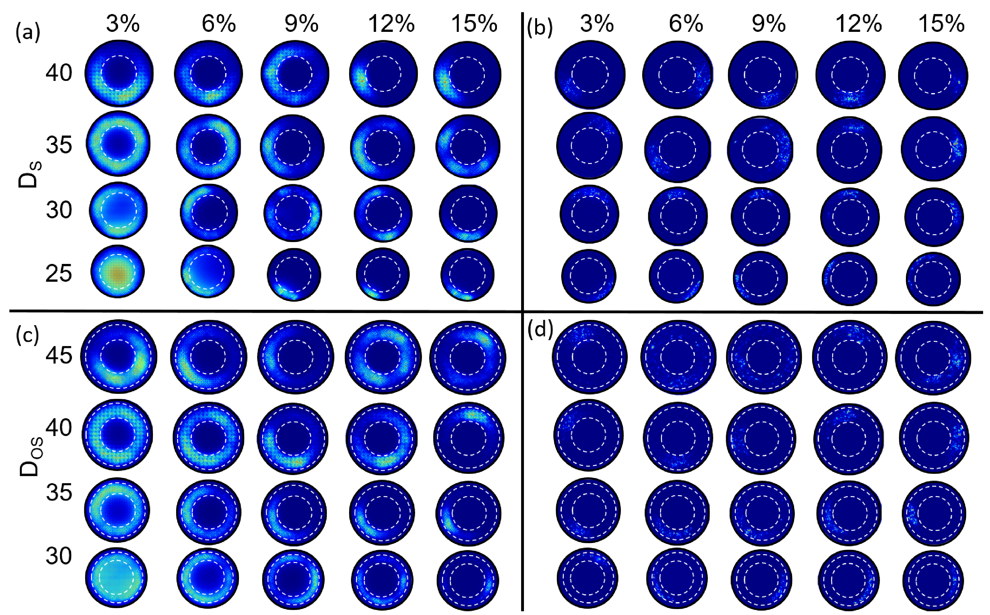
The inter-band optical absorption strength depends on the spatial profiles of the confined electron and hole charge carriers in the nanowire region. Figure 3 (a) and (b) plots the spatial distribution of the lowest electron and the highest hole states through a [001] plane at the center of the GaBixAs1-x/GaAs nanowire region. The dashed white circles indicate the boundary of the GaAs core region. Notably, our calculations show that at 3% Bi composition and small nanowire diameters (25 nm), the electron wave function is confined inside the GaAs core region and the hole wave function is confined in the GaBixAs1-x shell region, leading to a quasi type-II confinement. This is attributed to a very small hydrostatic strain as shown in the Figure 2 (a), which leads to a negligibly small potential barrier for the electrons and therefore a significant leakage of the electron wave function in the GaAs region is computed. Overall, the calculations indicate that at 3% Bi fraction, the electron wave function is distributed inside the large part of the nanowire region but becomes highly confined at larger Bi fractions. This can be understood from the strain profiles plotted in Figure 3 (a) and (b). For small nanowire diameters, the hydrostatic strain inside the GaAs core region is relatively small compared to GaBixAs1-x shell region. Therefore, the electron wave functions experience a small potential barrier at the GaAs and GaBixAs1-x interface and some wave function leakage is expected in the core region. However, when the nanowire diameter is increased, the magnitude of the hydrostatic strain drastically increases in the GaAs core region, leading to a very large potential barrier which prohibits any electron wave function leakage inside the core region. Therefore, the electron wave functions are much more confined inside the shell region.
In comparison to the electron wave functions, the hole wave functions are impacted by both strain and alloy composition (pairs and clusters of Bi atoms) 52. Previous studies on bismuth-containing nanowires 38 and quantum wells 62, 40 have shown that the effect of alloy composition is stronger than the strain effect and therefore, the hole wave functions are heavily confined in the regions of Bi related clusters. In Figure 3 (b), we observe the same trend and the results show highly confined hole wave functions inside the GaBixAs1-x shell regions.
The effect of the GaAs outer shell region on charge carrier confinements is shown in Figures 3 (c) and (d), where we plot the lowest electron and the highest hole wave functions in the [001] plane through the center of the GaAs/GaBixAs1-x/GaAs nanowires for various diameters and Bi compositions. Overall, the effect of the GaAs outer shell is weak and the confinement of the electron and holes wave functions exhibit a very similar trend as noted earlier for the GaBixAs1-x/GaAs nanowires. Again, for 3% Bi fraction and 30 nm nanowire diameter, we compute a type-II confinement where the electron wave function is inside the GaAs core region and the hole wave function is confined inside the GaBixAs1-x shell region. As the diameter of nanowire is increased with fixed Bi composition, the electron wave function gradually becomes more confined inside the GaBixAs1-x shell region and the nanowire exhibits a type-I confinement. For the highest Bi composition (15%), we find a strong electron wave function confinement inside the GaBixAs1-x shell region irrespective of nanowire diameter. The hole wave functions are again dominated by the Bi clustering effect and therefore exhibit a strong confinement inside the GaBixAs1-x shell region at all of the investigated diameters and compositions.
Polarisation-sensitive Light Absorption
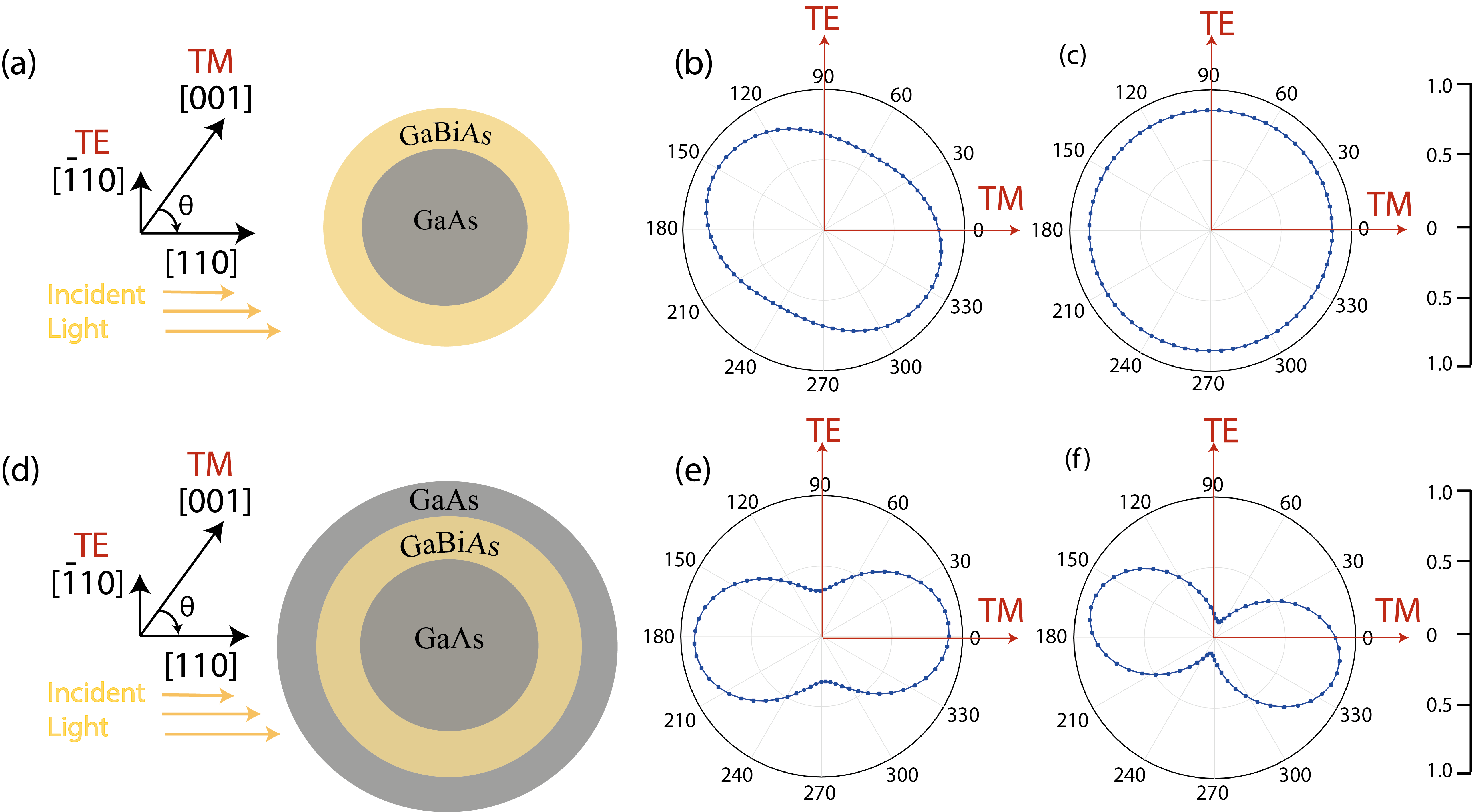
The polarisation sensitivity of the inter-band optical transitions is an important parameter of interest for many photonic devices. In the past studies, this parameter has been investigated for many nanostructures, including quantum dots 63, quantum dot molecules 60, quantum dot stacks 61, 64, 65, nanowires 66, 67, and nanorods 68, 69. The polarisation response of a nanostructure is characterised in terms of polarisation ratio or degree of polarization (DOP) which is defined as , where TE is transverse electric mode and TM is traverse magnetic mode of the incident polarised light.
Generally, for a lattice mismatched nanostructure where a large lattice constant material such as InAs is surrounded by a small lattice constant material such as GaAs, the strong compressive biaxial strain leads to high sensitivity of the light absorption towards TE mode polarisation 70, 64, resulting in DOP values closer to 1. This is because the highly compressive biaxial strain shifts HH band towards higher energies and the LH band towards the lower energies, leading to the top-most valence band states dominated by HH character, which only couples to the TE mode. For polarisation-insensitive light interaction (i.e. DOP=0), nanostructures are engineered to achieve tensile biaxial strain such that the LH mixing of the valence band increases TM mode coupling. This, for example, has been done in the past for large quantum dot stacks 61, 65, 64, where DOP values close to zero are reported both from experimental measurements and theoretical simulations. Here, in this work, we have shown that the biaxial strain is tensile inside the GaBixAs1-x shell region which naturally increases the LH character of the top-most hole states. As a result, a much larger TM mode coupling is expected for the investigated nanowires.
Figure 4 plots the polarisation dependent optical transition strengths for a selected set of nanowires with 15% Bi composition, which are relevant for telecommunication wavelength photonic devices. The incident light direction is assumed along the [110] direction, and the polarisation angle is varied between the [001] and [10] directions, where 0 angle indicates TM mode strength and 90 angle indicates TE mode strength. In all cases, we find a very strong TM mode strength which is a direct consequence of the LH mixing in the valence band states. Interestingly, we discover that for 15% Bi composition, the GaBixAs1-x/GaAs nanowire with 40 nm diameter exhibits a polarisation-insensitive light absorption (TE TM). This is very promising as the same nanowire has band-gap wavelength of 1550 nm which is directly relevant for the telecommunication wavelength devices. We also note that overall the polarisation response of GaBixAs1-x/GaAs nanowires is more isotropic compared to the polarisation response of GaAs/GaBixAs1-x/GaAs nanowires, the latter being more dominated by TM mode. This is due to the biaxial strain profile studied earlier in Figures 2 (b) and (e), where the tensile biaxial strain is relatively stronger for the GaAs/GaBixAs1-x/GaAs nanowires which will result in higher mixing of LH band in the highest valence band states.
Summary and Outlook
In summary, this work has investigated the optoelectronic properties of GaBixAs1-x/GaAs and GaAs/GaBixAs1-x/GaAs coreshell nanowires by carrying out a systematic set of multi-million atom tight-binding calculations. The results show a highly tunable band-gap energy which can be engineered by either controlling the nanowire diameter or by adjusting the Bi composition in the shell region. Due to highly mismatched lattice parameters of GaAs and GaBixAs1-x materials, the strain is expected to have an impact comparable to quantum confinement, provided the interface remains relatively defect free and coherent. Remarkably, the detailed analysis of the internal strain profiles reveals a peculiar character which is found to profoundly impact the charge carrier confinements and sensitivity to light polarisation. The controllability of strain magnitude by Bi fractions and nanowire diameters allows modification of carrier confinements from a quasi type II to highly confined type I character, which broadens the scope of the investigated nanowires for myriad applications involving large carrier separations or strong inter-band optical transition strengths. A polarisation-dependent optical spectrum is computed which exhibits high TM mode coupling due to highly tensile strain character inside the GaBixAs1-x shell region. We also report the possibility of realising isotropic polarisation response at 1550 nm wavelength, which is highly desirable for many photonics devices such as optical amplifiers. Overall, our analysis uncovers important physical factors which impact the optoelectronic character of coreshell nanowires for investigated constituent materials and geometries, which can aid in the advancement of ongoing experimental efforts to incorporate GaBixAs1-x materials in the active region of nanowires.
The idea of including GaBixAs1-x material in nanowires is relatively new, with the first experimental study published only recently 19. However, there is rapidly growing research interest in this novel material system as demonstrated by the subsequent experimental studies in the last few years showing promising progress 20, 21, 22, 23, 24, 25, 26. One of the critical challenges in the next few years will be to incorporate large Bi fractions in the active region of nanowire to achieve optical wavelengths to target photonic devices working in the near to mid and far infra-red regimes. For example as predicted in this work, the photonic devices aimed at the telecommunication applications would require Bi fractions in the range of 10 to 15%. In the first experimental effort, about 2% Bi was reported 19 but recently upto 10% Bi has been incorporated in the nanowire structure 23. We hope this study will further inspire and instigate experimental efforts to achieve larger Bi fractions. In short term with low Bi compositions ( 3%), these nanowires could also be explored for devices requiring quasi type II carrier confinements. We also note that there are other highly-mismatched bismuth-containing alloys such as GaSbBi, GaBiNAs, and InGaBiAs, which have been investigated in the literature and have shown very similar properties as observed for the GaBiAs alloy 30, 71, 72, 40, 73. Although this work is focused only on the GaBixAs1-x material, it would be interesting to explore the optoelectronic properties of coreshell nanowires for a range of bismide materials in conjunction with experimental efforts.
Methods
The electronic structure atomistic simulations performed in this work are based on a well-benchmarked tight-binding model 29, which have been verified against a number of experimental studies . The subsequent density functional theory calculations and experimental studies have also confirmed the accuracy of our tight-binding model. The tight-binding Hamiltonian is based on ten-band sp3s∗ model including spin orbit coupling and is implemented within the framework of nanoelectronic modeling tool NEMO3D 53. The diagonalisation of the tight-binding Hamiltonian at the point provides electron and hole energies and wave functions which are plotted in Figures 1 and 3. Due to the lattice mismatch between GaAs and GaBixAs1-x materials, the atoms are displaced from their original lattice and lead to strain inside the nanostructure. The computation of strain is based on atomistic valence force field relaxation scheme 57, where we have employed the experimentally reported bulk lattice constants and elastic coefficients for the GaAs and GaBi materials 29. The corresponding strain profiles are plotted in the Figure 2. The inter-band optical transition strengths between the electron and hole wave functions are computed by using the Fermi’s golden rule as follows: first we calculated squared absolute values of the momentum matrix elements summed over spin degenerate states, T = where is the single particle tight binding Hamiltonian in the basis, and are the electron and hole energy states respectively, and is a vector along the polarization direction. The polarization dependent polar plots are computed by rotating the polarization vector = to the appropriate direction in the polar coordinates: and is varied from 0 to 360o.
Computational resources are acknowledged from the National Computational Infrastructure (NCI) and Pawsey Supercomputer Center under the National Computational Merit based Allocation Scheme (NCMAS).
References
- Dasgupta et al. 2014 Dasgupta, N.; Sun, J.; Liu, C.; Brittman, S.; Andrews, S.; Lim, J.; Gao, H.; Yan, R.; Yang, P. 25th Anniversary Article: Semiconductor Nanowires Synthesis, Characterization, and Applications. Adv. Mater. 2014, 26, 2137
- Zhuang et al. 2011 Zhuang, X.; Ning, C.; Pan, A. Composition and BandgapGraded Semiconductor Alloy Nanowires. Adv. Mater. 2011, 24, 13
- Yao et al. 2013 Yao, J.; Yan, H.; Lieber, C. A nanoscale combing technique for the large-scale assembly of highly aligned nanowires. Nature Nanotechnology 2013, 8, 329
- Tomioka et al. 2012 Tomioka, K.; Yoshimura, M.; Fukui, T. A IIIV nanowire channel on silicon for high-performance vertical transistors. Nature 2012, 488, 189
- Chen et al. 2011 Chen, R.; Tran, T.-T.; Ng, K.; Ko, W.; Chuang, L.; Sedgwick, F.; C.-Hasnain, C. Nanolasers grown on silicon. Nature Photonics 2011, 5, 170
- Wang et al. 2003 Wang, D.; Song, J.; Mu, Y.; Lieber, C.; Whang, M.; Jin, S.; Wu, Y.; Lieber, M. Large-scale hierarchical organisation of nanowire arrays for integrated nanosystems. Nano Lett. 2003, 3, 1255
- Yan et al. 2009 Yan, R.; Gargas, D.; Yang, P. Nanowire Photonics. Nature Photonics 2009, 3, 569
- Eaton et al. 2016 Eaton, S.; Fu, A.; Wong, A.; Ning, C.-Z.; Yang, P. Semiconductor nanowire lasers. Nature Reviews Materials 2016, 1, 16028
- Cartoixa et al. 2017 Cartoixa, X.; Palummo, M.; Hauge, H. T.; Bakkers, E. P. A. M.; Rurali, R. Optical Emission in Hexagonal SiGe Nanowires. Nano Lett. 2017, 17, 4753
- Zhao et al. 2020 Zhao, X.; Nagashima, K.; Zhang, G.; Hosomi, T.; Yoshida, H.; Akihiro, Y.; Kanai, M.; Mizukami, W.; Zhu, Z.; Takahashi, T.; Suzuki, M.; Samransuksamer, B.; Meng, G.; Yasui, T.; Aoki, Y. Synthesis of Monodispersedly Sized ZnO Nanowires from Randomly Sized Seeds. Nano Lett. 2020, 20, 599
- Dimakis et al. 2014 Dimakis, E.; Jahn, U.; Ramsteiner, M.; Tahraoui, A.; Grandal, J.; Kong, X.; Marquardt, O.; Trampert, A.; Riechert, H.; Geelhaar, L. Coaxial Multishell (In,Ga)As/GaAs Nanowires for Near-Infrared Emission on Si Substrates. Nano Lett. 2014, 14, 2604
- Munshi et al. 2012 Munshi, A.; Dheeraj, D.; Fauske, V.; Kim, D.-C.; van Helvoort, A.; Fimland, B.-O.; Weman, H. Vertically Aligned GaAs Nanowires on Graphite and Few-Layer Graphene: Generic Model and Epitaxial Growth. Nano Lett. 2012, 12, 4570
- Royo et al. 2017 Royo, M.; Luca, M.; Rurali, R.; Zardo, I. A review on IIIV coremultishell nanowires: growth, properties, and applications. J. Phys. D: Appl. Phys. 2017, 50, 143001
- Balagula et al. 2020 Balagula, R.; Jansson, M.; Yukimune, M.; Stehr, J.; Ishikawa, F.; Chen, W.; Buyanova, I. Effects of thermal annealing on localization and strain in core/ multishell GaAs/GaNAs/GaAs nanowires. Sci. Rep. 2020, 10, 8216
- Kim et al. 2006 Kim, Y.; Joyce, H.; Gao, Q.; Tan, H.; Jagadish, C.; Paladugu, M.; Zou, J.; Suvorova, A. Influence of Nanowire Density on the Shape and Optical Properties of Ternary InGaAs Nanowires. Nano Lett. 2006, 6, 599
- Ren et al. 2014 Ren, P.; Hu, W.; Zhang, Q.; Zhu, X.; Zhuang, X.; Ma, L.; Fan, X.; Liao, H.; Duan, X.; Pan, A. BandSelective Infrared Photodetectors with CompleteCompositionRange InAsxP1-x Alloy Nanowires. Adv. Mater. 2014, 26, 7444
- Ma et al. 2014 Ma, L.; Hu, W.; Zhang, Q.; Ren, P.; Zhuang, X.; Zhou, H.; Xu, J.; Li, H.; Shan, Z.; Wang, X.; Liao, L.; Xu, H.; Pan, A. Room-Temperature Near-Infrared Photodetectors Based on Single Heterojunction Nanowires. Nano Lett. 2014, 14, 694
- Dai et al. 2014 Dai, X.; Zhang, S.; Wang, Z.; Adamo, G.; Liu, H.; Huang, Y.; Couteau, C.; Soci, C. GaAs/AlGaAs Nanowire Photodetector. Nano Lett. 2014, 14, 2688
- Ishikawa et al. 2015 Ishikawa, F.; Akamatsu, Y.; Watanabe, K.; Uesugi, F.; Asahina, S.; Jahn, U.; Shimomura, S. Metamorphic GaAs/GaAsBi Heterostructured Nanowires. Nano Letters 2015, 15, 7265
- Steele et al. 2016 Steele, J. A.; Lewis, R. A.; Horvat, J.; Nancarrow, M. J. B.; Henini, M.; Fan, D.; Mazur, Y. I.; Schmidbauer, M.; Ware, M. E.; Yu, S.-Q.; Salamo, G. J. Surface effects of vapour-liquid-solid driven Bi surface droplets formed during molecular-beam-epitaxy of GaAsBi. Sci. Rep. 2016, 6, 28860
- Zelewski et al. 2016 Zelewski, S.; Kopaczek, J.; Linhart, W. M.; Ishikawa, F.; Shimomura, S.; Kudrawiec, R. Photoacoustic spectroscopy of absorption edge for GaAsBi/GaAs nanowires grown on Si substrate. Appl. Phys. Lett. 2016, 109, 182106
- Wang et al. 2016 Wang, P.; Pan, W.; Wu, X.; Cao, C.; Wang, S.; Gong, Q. Heteroepitaxy growth of GaAsBi on Ge(100) substrate by gas source molecular beam epitaxy. Appl. Phys. Express 2016, 9, 045502
- Oliva et al. 2019 Oliva, M.; Gao, G.; Luna, E.; Geelhaar, L.; Lewis, R. Axial GaAs/Ga(As,Bi) Nanowire Heterostructures. Nanotechnology 2019, 30, 425601
- Zhang et al. 2019 Zhang, B.; Huang, Y.; Stehr, J. E.; Chen, P.-P.; Wang, X.-J.; Lu, W.; Chen, W. M.; Buyanova, I. A. Band Structure of Wurtzite GaBiAs Nanowires. Nano Lett. 2019, 19, 6454
- Matsuda et al. 2019 Matsuda, T.; Takada, K.; Yano, K.; Tsutsumi, R.; Yoshikawa, K.; Shimomura, S.; Shimizu, Y.; Nagashima, K.; Yanagida, T.; Ishikawa, F. Controlling Bi-Provoked Nanostructure Formation in GaAs/GaAsBi Core-Shell Nanowires. Nano Lett. 2019, 19, 8510
- Matsuda et al. 2019 Matsuda, T.; Takada, K.; Yano, K.; Shimomura, S.; Ishikawa, F. Strain deformation in GaAs/GaAsBi core-shell nanowire heterostructures. J. Appl. Phys. 2019, 125, 194301
- Janotti et al. 2002 Janotti, A.; Wei, S.-H.; Zhang, S. B. Theoretical study of the effects of isovalent coalloying of Bi and N in GaAs. Phys. Rev. B 2002, 65, 115203
- Zhang et al. 2005 Zhang, Y.; Mascarenhas, A.; Wang, L.-W. Similar and dissimilar aspects of IIIV semiconductors containing Bi versus N. Phys. Rev. B 2005, 71, 155201
- Usman et al. 2011 Usman, M.; Broderick, C. A.; Lindsay, A.; O’Reilly, E. P. Tight-binding analysis of the electronic structure of dilute bismide alloys of GaP and GaAs. Phys. Rev. B 2011, 84, 245202
- Li and Wang 2013 Li, H., Wang, Z., Eds. Bismuth-Containing Compounds; Springer-Verlag New York, 2013
- Broderick et al. 2017 Broderick, C. A.; Marko, I. P.; O’Reilly, E. P.; Sweeney, S. J. “Dilute Bismide Alloys”, Chapter 10 – Handbook of Optoelectronic Device Modeling and Simulation (Vol. 1), in press 2017,
- Fluegel et al. 2006 Fluegel, B.; Francoeur, S.; Mascarenhas, A.; Tixier, S.; Young, E.; Tiedje, T. Giant Spin-Orbit Bowing in GaAs1-xBix. Phys. Rev. Lett. 2006, 97, 067205
- Tumenas et al. 2012 Tumenas, S.; Karpus, V.; Bertulis, K.; Arwin, H. Dielectric function and refractive index of GaBixAs1-x (x = 0.035, 0.052, 0.075). Phys. Status Solidi c 2012, 9, 1633
- Batool et al. 2012 Batool, Z.; Hild, K.; Hosea, T. J. C.; Lu, X.; Tiedje, T.; Sweeney, S. J. The electronic band structure of GaBiAs/GaAs layers: Influence of strain and band anti-crossing. J. Appl. Phys. 2012, 111, 113108
- Phillips et al. 1999 Phillips, A. F.; Sweeney, S. J.; Adams, A. R.; Thijs, P. J. A. The temperature dependence of 1.3- and 1.5-m compressively strained InGaAs(P) MQW semiconductor lasers. IEEE J. Sel. Top. Quantum Electron. 1999, 5, 401
- Sweeney et al. 1999 Sweeney, S. J.; Adams, A. R.; Silver, M.; O’Reilly, E. P.; Watling, J. R.; Walker, A. B.; Thijs, P. J. A. Dependence of threshold current on QW position and on pressure in 1.5 m InGaAs(P) lasers. Phys. Status Solidi B 1999, 211, 525
- Broderick et al. 2012 Broderick, C. A.; Usman, M.; Sweeney, S. J.; O’Reilly, E. P. Band engineering in dilute nitride and bismide semiconductor lasers. Semicond. Sci. Technol. 2012, 27, 094011
- Usman 2019 Usman, M. Towards low-loss telecom-wavelength photonic devices by designing GaBiAs/GaAs core-shell nanowires. Nanoscale 2019, 11, 20133
- Usman et al. 2013 Usman, M.; Broderick, C. A.; Batool, Z.; Hild, K.; Hosea, T. J. C.; Sweeney, S. J.; O’Reilly, E. P. Impact of alloy disorder on the band structure of compressively strained GaBixAs1-x. Phys. Rev. B 2013, 87, 115104
- Usman et al. 2018 Usman, M.; Broderick, C. A.; O’Reilly, E. P. Impact of disorder on the optoelectronic properties of GaNyAs1-x-yBix alloys and heterostructures. Phys. Rev. Applied 2018, 10, 044024
- Kudrawiec et al. 2014 Kudrawiec, R.; Kopaczek, J.; Polak, M.; Scharoch, P.; Gladysiewicz, M.; Misiewicz, J.; Richards, R.; Bastiman, F.; David, J. J. Appl. Phys. 2014, 116, 233508
- Polak et al. 2015 Polak, M. P.; Scharoch, P.; Kudrawiec, R. Semicond. Sci. Technol. 2015, 30, 094001
- Bannow et al. 2016 Bannow, L. C.; Rubel, O.; Badescu, S.; Rosenow, P.; Hader, J.; Moloney, J.; Tonner, R.; Koch, S. Phys. Rev. B 2016, 93, 205202
- Donmez et al. 2015 Donmez, O.; Erol, A.; Arikan, M.; Makhloufi, H.; Arnoult, A.; Fontaine, C. Semicond. Sci. Technol. 2015, 30, 094016
- Balanta et al. 2017 Balanta, M. A. G.; Gordo, V. O.; Carvalho, A. R. H.; Puustinen, J.; Alghamdi, H. M.; Henini, M.; Galeti, H. V. A.; Guina, M.; Gobato, Y. G. Polarization resolved photoluminescence in GaAs1-xBix/GaAs quantum wells. J. of Luminescence 2017, 182, 49–52
- Zhang et al. 2018 Zhang, B.; Qiu, W.-Y.; Chen, P.-P.; Wang, X.-J. J. Appl. Phys. 2018, 123, 035702
- Dybala et al. 2017 Dybala, F.; Kopaczek, J.; Gladysiewicz, M.; Pavelescu, E.-M.; Romanitan, C.; Ligor, O.; Arnoult, A.; Fontaine, C.; Kudrawiec, R. J. of Appl. Phys. 2017, 111, 192104
- Collar et al. 2017 Collar, K.; Li, J.; Jiao, W.; Guan, Y.; Losurdo, M.; Humlicek, J.; Brown, A. S. AIP Advances 2017, 7, 075016
- Broderick et al. 2014 Broderick, C. A.; Mazzucato, S.; Carrère, H.; Amand, T.; Makhloufi, H.; Arnoult, A.; Fontaine, C.; Donmez, O.; Erol, A.; Usman, M.; O’Reilly, E. P.; Marie, X. Anisotropic electron g factor as a probe of the electronic structure of GaBixAs1-x/GaAs epilayers. Phys. Rev. B 2014, 90, 195301
- Broderick et al. 2013 Broderick, C. A.; Usman, M.; O’Reilly, E. P. Derivation of 12 and 14-band kp Hamiltonians for dilute bismide and bismide-nitride alloys. Semicond. Sci. Technol. 2013, 28, 125025
- Broderick et al. 2015 Broderick, C. A.; Harnedy, P. E.; Ludewig, P.; Bushell, Z. L.; Volz, K.; Manning, R. J.; O’Reilly, E. P. Determination of type-I band offsets in GaBixAs1-x quantum wells using polarisation-resolved photovoltage measurements and 12-band kp calculations. Semicond. Sci. Technol. 2015, 30, 094009
- Usman and O’Reilly 2014 Usman, M.; O’Reilly, E. P. Atomistic tight-binding study of electronic structure and interband optical transitions in GaBiAs/GaAs quantum wells. Appl. Phys. Lett. 2014, 104, 071103
- Klimeck et al. 2007 Klimeck, G.; Ahmed, S. S.; Kharche, N.; Korkusinski, M.; Usman, M.; Prada, M.; Boykin, T. Atomistic simulation of realistically sized nanodevices using NEMO 3-D – part I: applications. IEEE Trans. Electron. Dev. 2007, 54, 2090
- Ahmed et al. 2009 Ahmed, S. et al. In Encyclopedia of Complexity and Systems Science; Meyers, R. A., Ed.; Springer New York: New York, NY, 2009; pp 5745–5783
- Qian et al. 2008 Qian, F.; Li, Y.; Gradecak, S.; Park, H.-G.; Dong, Y.; Ding, Y.; Wang, Z. L.; Lieber, C. Multi-quantum-well nanowire heterostructures for wavelength-controlled lasers. Nature Materials 2008, 7, 701
- Usman et al. 2009 Usman, M.; Ryu, H.; Woo, I.; Ebert, D.; Klimeck, G. Moving toward nano-TCAD through multimillion-atom quantum-dot simulations matching experimental data. IEEE Trans. Nanotech. 2009, 8, 330
- Keating 1966 Keating, P. N. Effect of invariance requirements on the elastic strain energy of crystals with application to the diamond structure. Phys. Rev. 1966, 145, 637
- Lee et al. 2004 Lee, S.; Lazarenkova, O. L.; von Allmen, P.; Oyafuso, F.; Klimeck, G. Effect of wetting layers on the strain and electronic structure of InAs self-assembled quantum dots. Phys. Rev. B 2004, 70, 125307
- Singh 1985 Singh, J. Role of interface roughness and alloy disorder in photoluminescence in quantum-well structures. J. Appl. Phys. 1985, 57, 5433
- Usman et al. 2011 Usman, M.; Heck, S.; Clarke, E.; Spencer, P.; Ryu, H.; Murray, R.; Klimeck, G. Experimental and theoretical study of polarization-dependent optical transitions in InAs quantum dots at telecommunication-wavelengths (1300-1500 nm). J. Appl. Phys. 2011, 109, 104510
- Usman et al. 2011 Usman, M.; Inoue, T.; Harda, Y.; Klimeck, G.; Kita, T. Experimental and atomistic theoretical study of degree of polarization from multilayer InAs/GaAs quantum dot stacks. Phys. Rev. B 2011, 84, 115321
- Usman 2018 Usman, M. Large-scale atomistic simulations demonstrate dominant alloy disorder effects in GaBiAs/GaAs multiple quantum wells. Phys. Rev. Materials 2018, 2, 044602
- Usman 2012 Usman, M. Atomistic theoretical study of electronic and polarization properties of single and vertically stacked elliptical InAs quantum dots. Phys. Rev. B 2012, 86, 155444
- Greif et al. 2018 Greif, L.; Jagsch, S.; Wagner, M.; Schliwa, A. Tuning the Emission Directionality of Stacked Quantum Dots. ACS Photonics 2018, 5, 12
- Inoue et al. 2010 Inoue, T.; Asada, M.; Yasuoka, N.; Kojima, O.; Kita, T.; Wada, O. . Appl. Phys. Lett. 2010, 96, 211906
- Wang et al. 2001 Wang, J.; Gudiksen, M.; Duan, X.; Cui, Y.; Lieber, C. Highly Polarized Photoluminescence and Photodetection from Single Indium Phosphide Nanowires. Phys. Rev. B 2001, 293, 1455
- Casadei et al. 2015 Casadei, A.; Llado, E. A.; Amaduzzi, F.; Russo-Averchi, E.; Ruffer, D.; Heiss, M.; Negro, L. D.; Morral, A. F. Polarization response of nanowires. Sci. Rep. 2015, 5, 7651
- Hadar et al. 2013 Hadar, I.; Hitin, G.; Sitt, A.; Faust, A.; Banin, U. Polarization Properties of Semiconductor Nanorod Heterostructures: From Single Particles to the Ensemble. J. Phys. Chem. Lett. 2013, 3, 502
- Zhi et al. 2016 Zhi, T.; Tao, T.; Liu, B.; Zhuang, Z.; Dai, J.; Li, Y.; Zhang, G.; Xie, Z.; Chen, P.; Zhang, R. Polarized Emission From InGaN/GaN Single Nanorod Light-Emitting Diode. IEEE Photonics Technology Letters 2016, 28, 721
- Usman 2011 Usman, M. In-plane polarization anisotropy of ground state optical intensity in InAs/GaAs quantum dots. J. Appl. Phys. 2011, 110, 094512
- Broderick et al. 2013 Broderick, C.; Usman, M.; O’Reilly, E. 12-band k.p model for dilute bismide alloys of (In)GaAs derived from supercell calculations. Physica Status Solidi (b) 2013, 250, 733
- Rajpalke et al. 2013 Rajpalke, M. K.; Linhart, W. M.; Birkett, M.; Yu, K. M.; Scanlon, D. O.; Buckeridge, J.; Jones, T. S.; Ashwin, M. J.; Veal, T. D. Growth and properties of GaSbBi alloys. Appl. Phys. Lett. 2013, 103, 142106
- Bushell et al. 2019 Bushell, Z.; Broderick, C.; Nattermann, L.; Joseph, R.; Keddie, J.; Rorison, J.; Volz, K.; Sweeney, S. Giant bowing of the band gap and spin-orbit splitting energy in GaP1−xBix dilute bismide alloys. Scientific Reports 2019, 9, 6835