Raman spectrum of Janus transition metal dichalcogenide monolayers
WSSe and MoSSe
Abstract
Janus transition metal dichalcogenides (TMDs) lose the horizontal mirror symmetry of ordinary TMDs, leading to the emergence of additional features, such as native piezoelectricity, Rashba effect, and enhanced catalytic activity. While Raman spectroscopy is an essential nondestructive, phase- and composition-sensitive tool to monitor the synthesis of materials, a comprehensive study of the Raman spectrum of Janus monolayers is still missing. Here, we discuss the Raman spectra of WSSe and MoSSe measured at room and cryogenic temperatures, near and off resonance. By combining polarization-resolved Raman data with calculations of the phonon dispersion and using symmetry considerations, we identify the four first-order Raman modes and higher-order two-phonon modes. Moreover, we observe defect-activated phonon processes, which provide a route toward a quantitative assessment of the defect concentration and, thus, the crystal quality of the materials. Our work establishes a solid background for future research on material synthesis, study, and application of Janus TMD monolayers.
I Introduction
Over the past decade, transition metal dichalcogenide (TMD) monolayers have emerged as a unique playground for exciton photophysics due to -eV-high exciton binding energies [1, 2], strong light-matter interaction [3, 4], optically addressable valley-contrasting spin physics caused by broken inversion symmetry [5], and large spin-orbit coupling [6]. Further studies also revealed the presence of quantum light emitters [7, 8, 9, 10, 11, 12] and evidence of strongly correlated phases such as superconductivity [13, 14] and exciton and polaron Bose-Einstein condensation [15, 16]. Integrability on conventional silicon photonic technology [17, 18], large-area fabrication [19, 20, 21] and deterministic positioning of quantum emitters [22, 23, 24] widen the impact of TMDs to optoelectronics [25] and energy harvesting [26] as well as applications exploiting valleytronics [27, 28], spintronics [29, 30, 31], and quantum photonic properties [32, 33]. In addition, new functionalities and physical phenomena appear when stacking monolayers of TMDs on top of each other, forming artificial metamaterials held together by van der Waals forces [34]. Such heterostructures host long-lived, tunable dipolar interlayer [35] and trapped moiré excitons [36, 37, 38, 39], offering a rich playground for few- and many-body phenomena [40, 41, 42, 43, 44, 45, 46], making them candidates for a solid-state quantum simulation platform [47].
In contrast to conventional, mirror-symmetric TMDs with a stoichiometric formula (where is a transition metal and is a chalcogen), Janus TMD monolayers are formed when the crystal plane of transition metal atoms is sandwiched between two planes, each made of a different chalcogen atom and . This breaks mirror symmetry along the direction perpendicular to the plane of the two-dimensional (2D) material, reducing the overall symmetry of the crystal, and gives rise to an intrinsic electrical dipole in the unit cell created by the difference in electronegativity between the top and bottom chalcogen atoms [48]. Consequently, theoretical studies predict the appearance of a multitude of physical phenomena such as piezoelectricity [49, 50], enhanced photocatalysis [51, 52, 53, 54], Rashba splitting [55, 56, 57], and the presence of topological phases [58]. However, most of these physical effects are still experimentally unexplored, due to the very recent success at synthesizing Janus crystals. First reports on the growth of Janus MoSSe appeared in 2017 [59, 60], followed by Janus WSSe [61, 62], and their heterostructures in 2020 [61].
Inelastic light scattering is a powerful, non-destructive tool to gain insight into the structural and electronic properties of materials [63, 64]. Each Raman spectrum of 2D materials is a unique fingerprint of a sample, shedding light on its crystal and electronic band structure [65], layer number [66], interlayer coupling [67, 68], doping [69], defect density [70], electron-phonon interaction [71], etc. Moreover, Raman spectroscopy can be used in situ during growth to distinguish a Janus monolayer from a disordered ternary alloy [72, 73, 74, 75, 76]. Thus, to synthesize high-quality Janus TMD crystals and unlock the predicted effects and applications it is crucial to have a detailed study of its vibrational spectrum. However, a comprehensive study of the Raman spectrum of Janus monolayers WSSe and MoSSe is lacking. Initial experimental measurements have given limited insight on the Raman spectrum of Janus TMD monolayers, suffering from incomplete [59] or even incorrect [60] assignments of the first-order modes and leaving all other features unidentified.
In this work, we calculate the phonon band structure of Janus WSSe and MoSSe monolayers and their phonon density of states (PhDOS), which we use to predict the Raman modes and their energies. Then, we measure the Raman spectra of both materials at room and cryogenic (10 K) temperature and two excitation wavelengths , closer to and farther from excitonic resonances. Further, we perform polarization-resolved Raman measurements at room temperature and . By comparing theory and experiments, we identify the first-order Raman modes. As the experimental spectra show rich features arising beyond the calculated first-order processes, we then discuss the mechanisms of higher-order and defect-mediated Raman modes and assign them to the relevant experimental peaks.
II Results and Discussion
Monolayers of conventional 2H-TMDs have space group symmetry [77, 78], contrasting strongly with Janus TMD monolayers, for which rotation , improper rotation , and mirror symmetries are broken due to the different chalcogen atoms in the unit cell. This results in a lowering of the symmetry of the crystal to the symmorphic (i.e., all symmetry operations leave one common point fixed) space group ( point group). The unit cell of the Janus monolayer is formed from three atoms, resulting in normal vibrational modes at the point (center) of the Brillouin zone, of which three are acoustic and six are optical. Group theory identifies these vibrations as the irreducible representations of the point group, that can be expressed by , where all of the modes are both Raman and infrared (IR) active. Here, is the irreducible representation of the total vibration, deduced from the underlying crystal symmetry using the character table. In-plane vibrations are defined as and out-of-plane as , with being doubly degenerate at the point (modes with the same symmetry are distinguished by the upper right corner index).
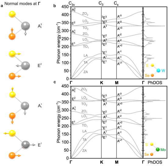
Owing to the conservation of energy and quasimomentum in the crystal, first-order (i.e., one-phonon) scattering processes are bound to the point of the Brillouin zone due to the negligible photon momentum (). The atomic displacements corresponding to the normal vibrational modes at are schematically represented in Fig. 1(a) with the transition metal atom in gray and the chalcogens Se and S in orange and yellow, respectively. We used density functional perturbation theory (DFPT) to predict the phonon modes (see Appendix A). In WSSe at the point, they occur at 204, 282, 331, and (for , , , and , respectively). Analogously, in MoSSe at the point, they occur at 208, 293, 358, and (for , , , and , respectively). This can be seen in the phonon band structure of monolayer WSSe in Fig. 1(b) and of monolayer MoSSe in Fig. 1(c). The three acoustic phonon branches correspond to the out-of-plane acoustic (ZA), the transverse acoustic (TA), and the in-plane longitudinal acoustic (LA) modes, respectively. The remaining six branches represent the out-of-plane optical (ZO1 and ZO2), the in-plane transverse optical (TO1 and TO2), and the in-plane longitudinal optical (LO1 and LO2) modes.
In addition to the point, we further examine the vibrational modes at high-symmetry points at the Brillouin zone edge, K and M (see Appendix B). At the K point, the crystal exhibits point group symmetry with the irreducible representation , where , , and are all Raman active modes. On the other hand, at the M point, the crystal exhibits point group symmetry with the irreducible representation , where and are both Raman active modes. Accompanied to the phonon dispersion in Figs. 1(b) and 1(c), the phonon density of states (PhDOS) reveals a high density of phonons at the flat bands, in particular close to the high-symmetry points K and M, with all phonons being Raman active. The dispersion branches of WSSe in Fig. 1(b) are energetically lower than the dispersion branches of MoSSe in Fig. 1(c), thus giving lower phonon energies at the same point in the Brillouin zone. This mainly occurs due to the larger atomic mass of W, which makes the vibrations softer, as in the case of regular Mo- and W-based TMDs [79]. The two materials also differ in the values of the phonon bandgaps (see Appendix C).
We measured the Raman spectra of Janus TMD monolayers recorded from crystals grown via room temperature selective epitaxy atomic replacement (SEAR) [61], as described in Appendix A. Here, the top-layer selenium atoms, in already grown and monolayers, are replaced by sulfur atoms, to eventually yield Janus TMD WSSe and MoSSe, respectively. WSSe was grown on , whereas MoSSe was grown on a substrate. We first conducted Raman spectroscopy in a back-scattering configuration, with a linearly polarized excitation and no polarization filtering of the Raman signal.
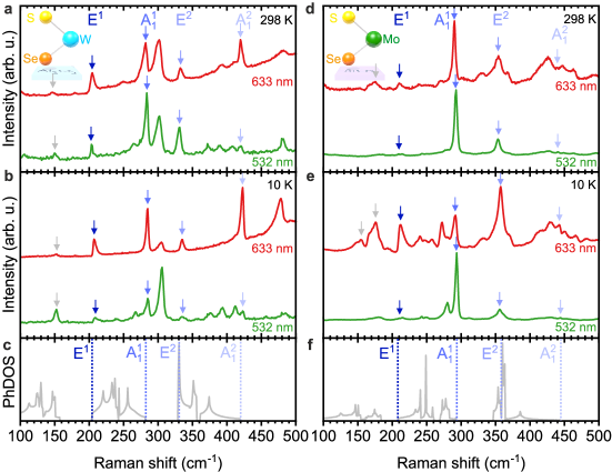
Figure 2 shows the Raman spectra of Janus monolayers WSSe and MoSSe between 100 and , collected with a laser excitation wavelength of (green curves) and (red curves), above the excitonic band gap at of both WSSe [61] () and MoSSe [59, 60, 61] () (see Appendix D). Figures 2(a) and 2(b) show typical Raman spectra recorded from Janus monolayer WSSe at room and cryogenic temperatures, respectively. From the comparison of Raman spectra at [Fig. 2(b)] with the calculated PhDOS in Fig. 2(c), where the dashed blue lines indicate the calculated values of phonons, we initially assign the first-order Raman modes at for ( for ), at (), at (), and at (). All predicted first-order Raman modes, indicated in the spectra by blue arrows, are visible in all experimental conditions, albeit their intensity is maximum at 10 K and for , which is close to the exciton resonance (top valence band to conduction band, see Appendix D). The experimental results closely match the theoretical predictions. For the spectra acquired at , we observe a broad background signal above , stemming from the photoluminescence tail of the material, due to the energetic proximity to the exciton transition. The Raman peaks at and at appear to be asymmetric, which can be attributed to phonon confinement effects due to an imperfect crystal quality [80, 81]. The experimental spectra also reveal a peak at , as indicated by gray arrows, which is especially strong at and , and corresponds to the position of the mode in the LA branch at the M point or the mode in the LA branch at the K point. These modes are expected to be silent in first-order Raman processes since their . We can exclude that this peak is caused by higher-order Raman modes due to its low energy and, therefore, attribute its appearance to defect-activation that relaxes the selection rule [82, 70].
The Raman spectra of Janus monolayer MoSSe are presented in Figs. 2(d) and 2(e), accompanied by the calculated PhDOS in Fig. 2(f). Analogously to Janus monolayer WSSe, we compare the spectra to the theoretically predicted phonon energies [Fig. 2(f), dashed blue lines] and initially assign the first-order Raman modes at for ( for ), at (), at (), and at (). Here, the spectra are strongly affected by the . First-order Raman modes, indicated by the blue arrows, are all clearly visible at , while two peaks are much weaker at . This arises once () is close to the exciton transition (bottom valence band to conduction band, see Appendix D), thereby increasing the Raman cross section. Again, we observe good agreement between theory and experiment, well within the error of the calculations. Also for MoSSe, peaks appear around 155 and for , as indicated by gray arrows, whose intensity is enhanced at 10 K. Similar to WSSe, the energy of the peaks in the range corresponds to the mode in the TA branch at the M point and to the and modes in the TA and ZA branches at the K point. The peaks in the range correspond to the mode in the LA branch at the M point and the mode at the K point in the LA branch. As discussed above, we exclude these peaks to be the result of higher-order Raman transitions due to their low energy, and instead attribute their appearance to defect activation. Interestingly, the presence of defect-activated Raman modes can be used to monitor the defect concentration in the crystal, in analogy to the D peak in graphene [82], and as such constitutes precious information to assess the crystal quality. The peak at corresponds to the mode in the first ZO branch at K. However, due to the presence of other non-double-resonant phonon combinations matching the same energy, its assignment requires further investigation. For completeness, all first-order Raman modes at are summarized in Table 1.
| Phonon mode | WSSe () | MoSSe () | |||||
|---|---|---|---|---|---|---|---|
| 298 K | 10 K | Theory | 298 K | 10 K | Theory | ||
| 633 nm | 204 | 207 | 204 | 210 | 212 | 208 | |
| 282 | 285 | 282 | 290 | 291 | 293 | ||
| 333 | 335 | 331 | 354 | 357 | 358 | ||
| 420 | 422 | 420 | 439 | 442 | 445 | ||
| 532 nm | 204 | 209 | 204 | 209 | 211 | 208 | |
| 284 | 285 | 282 | 292 | 293 | 293 | ||
| 331 | 336 | 331 | 354 | 356 | 358 | ||
| 420 | 423 | 420 | 441 | 444 | 445 | ||
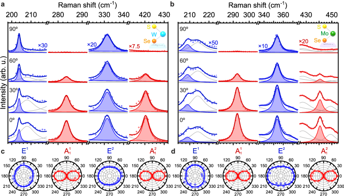
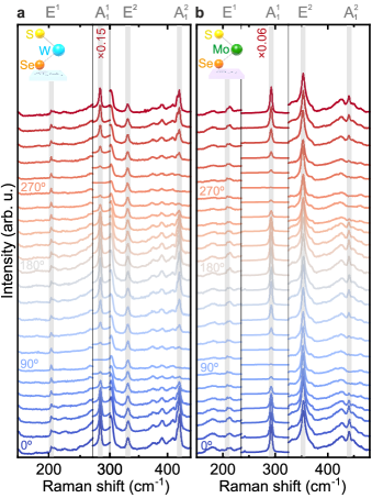
To further confirm the peaks’ assignments, we performed linear polarization-dependent Raman scattering measurements at room temperature and (see Appendix A for details). Figures 3(a) and 3(b) show the Raman spectra of Janus monolayers WSSe and MoSSe, respectively, for four representative angles between the excitation and detection polarization, starting from 0∘ (copolarized configuration) to 90∘ (cross-polarized configuration). The experimental data (dots) are fitted with a sum of Lorentzians (blue and red thick curves). Going from co- to cross polarization, the intensity of the blue peaks (initially assigned as modes) remains overall constant, while the intensity of the red peaks (initially assigned as modes) decreases from the maximum at 0∘ to zero at 90∘. Figures 3(c) and 3(d) show the polar plots of the fitted peak intensities of Janus monolayers WSSe and MoSSe as a function of the angle between excitation and detection linear polarizer for the complete data set acquired (see Appendix E for all raw spectra). Due to their symmetry, Raman selection rules predict the intensity of the modes to be independent from the linear polarization angle as , while the intensities of modes are predicted to be polarized following , where and are constants and is the angle. Thus, linearly polarized Raman spectra confirm our initial peaks’ assignments.
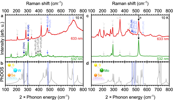
To explore higher-order Raman peaks, in Figs. 4(a) and 4(c) we plot the Raman spectra of Janus monolayers WSSe and MoSSe at 10 K between 100 and , and compare them to the PhDOS as a function of twice the phonon energy in Figs. 4(b) and 4(d). This is motivated by the role of double-resonant Raman scattering [83] in higher-order Raman transitions. In double-resonant Raman scattering, two phonons with the same momentum but opposite direction make electrons scatter far from their excitation point in the Brillouin zone and then come back to the initial position, through two resonant and two nonresonant scattering events, satisfying . Double-resonant Raman processes in WSSe and MoSSe are indicated by blue arrows in Figs. 4(a) and 4(c). Higher-order scattering processes that include phonons from different branches are also energetically allowed through defect activation that locally breaks crystal symmetries (dark gray arrows). A comprehensive assignment list of the observed higher-order Raman peaks is given in Table 2. The unassigned peaks which do not match with double-resonant processes may be defect activated, however, further studies are required to elucidate their nature.
| WSSe | MoSSe | |||
|---|---|---|---|---|
| Peak (cm-1) | Assignments | Peak (cm-1) | Assignments | |
| 2TA(K) | 466 | 2TO1(M) | ||
| 305 | 2LA(M) | 482 | 2TO1(K) | |
| TA+ZO1(K) | 497 | 2LO1(M) | ||
| LA+TO1(K) | 564 | 2ZO1(M) | ||
| LA+ZO1(M) | ||||
| 478 | 2LO1(K) | |||
| 491 | 2ZO1(K) | |||
| 709 | 2LO2(M) | |||
III Conclusion
In summary, we presented a combined theoretical and experimental study of the Raman modes of Janus monolayers WSSe and MoSSe, whereby we found excellent agreement between the two for the frequencies of first- and higher-order modes. Moreover, we discovered the presence of defect activation of otherwise silent Raman modes, which may be used as markers for assessing crystal quality in further studies.
The recent synthesis of Janus monolayer TMDs adds an extra degree of freedom to the wide family of two-dimensional and layered materials, with the potential for tunable, strongly interacting dipolar excitons in single-layer materials as the stepping stone for further exploration of correlated many-body states, exciton transport, and applications that exploit such features. However, novel physics and exciting new applications require in-depth information over the materials’ properties and growth quality, with Raman spectroscopy being a widely utilized technique in a such regard due to its descriptive power and simplicity of use and interpretation. Our work sets a general and much-needed reference over the vibrational properties of Janus monolayers, provides a starting point for further investigations on the role of phonons in such materials, and enables the benchmarking of future crystal growth attempts.
Acknowledgements.
M.M.P., M.K., and M.B. contributed equally to this work. M.B., J.J.F., A.R.B.-M., and K.M. conceived and managed the project. Y.Q., Y.Sa., Y.Sh., and S.T. grew the Janus TMD monolayers. M.M.P., M.K., and M.B. performed the optical measurements and analyzed the data. A.R.B.-M. performed DFPT calculations. All authors participated in the discussion of the results and the writing of the manuscript. We thank Moritz Meyer for technical assistance. S.T. acknowledges support from NSF DMR-1955889, NSF CMMI-1933214, NSF DMR-1552220, and DOE-SC0020653. K.M. and J.J.F. acknowledge support from the European Union Horizon 2020 research and innovation programme under Grant Agreement No. 820423 (S2QUIP) and the Deutsche Forschungsgemeinschaft (DFG, German Research Foundation) under Germany’s Excellence Strategy – MCQST (EXC-2111) and e-Conversion (EXC-2089). M.M.P. acknowledges TUM International Graduate School of Science and Engineering (IGSSE). M.K. acknowledges support from the International Max Planck Research School for Quantum Science and Technology (IMPRS-QST). M.B. acknowledges support from the Alexander von Humboldt Foundation. K.M. acknowledges support from the Bayerische Akademie der Wissenschaften. A.R.B.-M. acknowledges support from DGTIC-UNAM Supercomputing Center under Project LANCAD-UNAM-DGTIC-359.APPENDIX A METHODS
A.1 DFPT
Phonon dispersion relations were calculated using density functional perturbation theory with the local-density approximation to the exchange-correlation function [84, 85]. The vacuum distance between neighboring layers was to describe isolated layers within the periodic boundary conditions. Norm-conserving pseudopotentials and a basis set defined from a energy cutoff of 105 Ry [86, 87] were used. The first Brillouin zone was sampled with a 15151 Monkhorst-Pack grid.
A.2 SEAR
The synthesis of Janus TMDs is carried out in a specially designed quartz chamber and a home-built inductively coupled plasma system. The plasma chamber consists of a 5-ft-long quartz tube with a 1-in. inner diameter suspended off-centered on a Lindberg Blue/M single-zone furnace. A copper coil with a length 1.5 in. consisting of about five turns were wound around the quartz tube. The end of the Cu coil is connected to a 100-W tunable rf source (SEREN R101) through a custom-designed impedance match network. One end of the quartz tube is connected to an Edwards vacuum pump while the other end is fitted with a hydrogen supply line. Hydrogen flow rate and the pressure within the chamber is regulated by means of a capacitance manometer and a pressure controller. For the synthesis of Janus TMDs, the reaction chamber is pumped down to a base pressure of 15 mTorr, after which the chamber was purged with 20-sccm H2 flow, maintaining an operation pressure at 300 mTorr. The plasma was generated with 15-W rf power, and the visible plasma tail position was marked on the quartz tube. For the SEAR process to create WSSe, chemical vapor deposition (CVD)-grown WSe2 was placed 4 cm upstream of the marked visible plasma tail position onto a quartz boat, and 2-g sulfur was placed 15 cm upstream of the H2 plasma tail. The plasma treatment lasted for 18 min. For the creation of MoSSe, the position of CVD-grown MoSe2 and S source were kept at the same position as WSSe, except the processing time was decreased to 8 min because of the lower Mo-Se bond energy. The SEAR process can also be set up to create a 2D Janus structure from sulfur-based TMDs and selenium precursors in a similar fashion by varying the processing parameters.
A.3 Optical setup
Raman and photoluminescence (PL) measurements were done using a custom-made confocal microscope in backscattering geometry. The excitation laser beam is focused on the sample by an objective with numerical aperture NA 0.75 to a diffraction-limited spot. For cryogenic measurements a He-flow cryostat (Cryovac) was used. The collected light is analyzed in a spectrometer (maximum point-to-point resolution 1.2 cm-1 for and 0.8 cm-1 for with a grating with 1200 lines/mm) coupled to a charged-coupled device (Horiba). Both incident () and scattered () light polarization vectors are placed in the plane, which is relevant to account for the Raman intensity (for the case of no polarization filtering in the detection path, ) [64]. Here, represents the Raman tensor, which is derived from the point group symmetry, and alongside the scattering configuration dictates the selection rules [88, 89]. For polarization-resolved Raman measurements, we excited the Janus crystals using fixed linearly polarized light at and room temperature, collecting the scattered light through a rotating half-waveplate and a fixed linear polarizer.
APPENDIX B JANUS TMDs IN SPACE
Figure 5 shows the Brillouin zone of the Janus TMDs. The zone center point has the same symmetry as the crystal, while the and high-symmetry points are subgroups with and symmetries, respectively.

APPENDIX C PHONON BAND GAPS
The phonon band structure of Janus TMD monolayers [Figs. 1(b) and 1(c), main text] reveals the gap of unaccessible phonons that separates acoustic from optical bands. WSSe and MoSSe exhibit and band gaps, respectively. Forbidden phonon energies occur also between optical bands (phonon band gaps of for WSSe and for MoSSe).
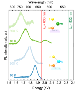
APPENDIX D PHOTOLUMINESCENCE OF WSSe AND MoSSe
APPENDIX E POLARIZATION-RESOLVED RAMAN SPECTRA
References
- Chernikov et al. [2014] A. Chernikov, T. C. Berkelbach, H. M. Hill, A. Rigosi, Y. Li, O. B. Aslan, D. R. Reichman, M. S. Hybertsen, and T. F. Heinz, Exciton binding energy and nonhydrogenic rydberg series in monolayer WS2, Physical Review Letters 113, 076802 (2014).
- Wang et al. [2018] G. Wang, A. Chernikov, M. M. Glazov, T. F. Heinz, X. Marie, T. Amand, and B. Urbaszek, Colloquium : Excitons in atomically thin transition metal dichalcogenides, Reviews of Modern Physics 90, 021001 (2018).
- Bernardi et al. [2013] M. Bernardi, M. Palummo, and J. C. Grossman, Extraordinary sunlight absorption and one nanometer thick photovoltaics using two-dimensional monolayer materials, Nano Letters 13, 3664 (2013).
- Wurstbauer et al. [2017] U. Wurstbauer, B. Miller, E. Parzinger, and A. W. Holleitner, Light–matter interaction in transition metal dichalcogenides and their heterostructures, Journal of Physics D: Applied Physics 50, 173001 (2017).
- Xiao et al. [2012] D. Xiao, G.-B. Liu, W. Feng, X. Xu, and W. Yao, Coupled spin and valley physics in monolayers of MoS2 and other group-VI dichalcogenides, Physical Review Letters 108, 196802 (2012).
- Zhu et al. [2011] Z. Y. Zhu, Y. C. Cheng, and U. Schwingenschlögl, Giant spin-orbit-induced spin splitting in two-dimensional transition-metal dichalcogenide semiconductors, Physical Review B 84, 153402 (2011).
- Tonndorf et al. [2015] P. Tonndorf, R. Schmidt, R. Schneider, J. Kern, M. Buscema, G. A. Steele, A. Castellanos-Gomez, H. S. J. van der Zant, S. Michaelis de Vasconcellos, and R. Bratschitsch, Single-photon emission from localized excitons in an atomically thin semiconductor, Optica 2, 347 (2015).
- Koperski et al. [2015] M. Koperski, K. Nogajewski, A. Arora, V. Cherkez, P. Mallet, J.-Y. Veuillen, J. Marcus, P. Kossacki, and M. Potemski, Single photon emitters in exfoliated WSe2 structures, Nature Nanotechnology 10, 503 (2015).
- Srivastava et al. [2015] A. Srivastava, M. Sidler, A. V. Allain, D. S. Lembke, A. Kis, and A. Imamoğlu, Optically active quantum dots in monolayer WSe2, Nature Nanotechnology 10, 491 (2015).
- Chakraborty et al. [2015] C. Chakraborty, L. Kinnischtzke, K. M. Goodfellow, R. Beams, and A. N. Vamivakas, Voltage-controlled quantum light from an atomically thin semiconductor, Nature Nanotechnology 10, 507 (2015).
- He et al. [2015] Y.-M. He, G. Clark, J. R. Schaibley, Y. He, M.-C. Chen, Y.-J. Wei, X. Ding, Q. Zhang, W. Yao, X. Xu, C.-Y. Lu, and J.-W. Pan, Single quantum emitters in monolayer semiconductors, Nature Nanotechnology 10, 497 (2015).
- Palacios-Berraquero et al. [2016] C. Palacios-Berraquero, M. Barbone, D. M. Kara, X. Chen, I. Goykhman, D. Yoon, A. K. Ott, J. Beitner, K. Watanabe, T. Taniguchi, A. C. Ferrari, and M. Atatüre, Atomically thin quantum light-emitting diodes, Nature Communications 7, 12978 (2016).
- Ye et al. [2012] J. T. Ye, Y. J. Zhang, R. Akashi, M. S. Bahramy, R. Arita, and Y. Iwasa, Superconducting dome in a gate-tuned band insulator, Science 338, 1193 (2012).
- Costanzo et al. [2016] D. Costanzo, S. Jo, H. Berger, and A. F. Morpurgo, Gate-induced superconductivity in atomically thin MoS2 crystals, Nature Nanotechnology 11, 339 (2016).
- Cotleţ et al. [2016] O. Cotleţ, S. Zeytinoǧlu, M. Sigrist, E. Demler, and A. Imamoǧlu, Superconductivity and other collective phenomena in a hybrid Bose-Fermi mixture formed by a polariton condensate and an electron system in two dimensions, Physical Review B 93, 054510 (2016).
- Kogar et al. [2017] A. Kogar, M. S. Rak, S. Vig, A. A. Husain, F. Flicker, Y. I. Joe, L. Venema, G. J. MacDougall, T. C. Chiang, E. Fradkin, J. van Wezel, and P. Abbamonte, Signatures of exciton condensation in a transition metal dichalcogenide, Science 358, 1314 (2017).
- Tonndorf et al. [2017] P. Tonndorf, O. Del Pozo-Zamudio, N. Gruhler, J. Kern, R. Schmidt, A. I. Dmitriev, A. P. Bakhtinov, A. I. Tartakovskii, W. Pernice, S. Michaelis de Vasconcellos, and R. Bratschitsch, On-chip waveguide coupling of a layered semiconductor single-photon source, Nano Letters 17, 5446 (2017).
- Youngblood and Li [2017] N. Youngblood and M. Li, Integration of 2D materials on a silicon photonics platform for optoelectronics applications, Nanophotonics 6, 892 (2017).
- Lee et al. [2012] Y.-H. Lee, X.-Q. Zhang, W. Zhang, M.-T. Chang, C.-T. Lin, K.-D. Chang, Y.-C. Yu, J. T.-W. Wang, C.-S. Chang, L.-J. Li, and T.-W. Lin, Synthesis of large-area MoS2 atomic layers with chemical vapor deposition, Advanced Materials 24, 2320 (2012).
- Zhan et al. [2012] Y. Zhan, Z. Liu, S. Najmaei, P. M. Ajayan, and J. Lou, Large-area vapor-phase growth and characterization of MoS2 atomic layers on a SiO2 substrate, Small 8, 966 (2012).
- Lee et al. [2013] Y.-H. Lee, L. Yu, H. Wang, W. Fang, X. Ling, Y. Shi, C.-T. Lin, J.-K. Huang, M.-T. Chang, C.-S. Chang, M. Dresselhaus, T. Palacios, L.-J. Li, and J. Kong, Synthesis and transfer of single-layer transition metal disulfides on diverse surfaces, Nano Letters 13, 1852 (2013).
- Palacios-Berraquero et al. [2017] C. Palacios-Berraquero, D. M. Kara, A. R.-P. Montblanch, M. Barbone, P. Latawiec, D. Yoon, A. K. Ott, M. Loncar, A. C. Ferrari, and M. Atatüre, Large-scale quantum-emitter arrays in atomically thin semiconductors, Nature Communications 8, 15093 (2017).
- Branny et al. [2017] A. Branny, S. Kumar, R. Proux, and B. D. Gerardot, Deterministic strain-induced arrays of quantum emitters in a two-dimensional semiconductor, Nature Communications 8, 15053 (2017).
- Klein et al. [2019] J. Klein, M. Lorke, M. Florian, F. Sigger, L. Sigl, S. Rey, J. Wierzbowski, J. Cerne, K. Müller, E. Mitterreiter, P. Zimmermann, T. Taniguchi, K. Watanabe, U. Wurstbauer, M. Kaniber, M. Knap, R. Schmidt, J. J. Finley, and A. W. Holleitner, Site-selectively generated photon emitters in monolayer MoS2 via local helium ion irradiation, Nature Communications 10, 2755 (2019).
- Ross et al. [2014] J. S. Ross, P. Klement, A. M. Jones, N. J. Ghimire, J. Yan, D. G. Mandrus, T. Taniguchi, K. Watanabe, K. Kitamura, W. Yao, D. H. Cobden, and X. Xu, Electrically tunable excitonic light-emitting diodes based on monolayer WSe2 p-n junctions, Nature Nanotechnology 9, 268 (2014).
- Pospischil et al. [2014] A. Pospischil, M. M. Furchi, and T. Mueller, Solar-energy conversion and light emission in an atomic monolayer p-n diode, Nature Nanotechnology 9, 257 (2014).
- Jones et al. [2013] A. M. Jones, H. Yu, N. J. Ghimire, S. Wu, G. Aivazian, J. S. Ross, B. Zhao, J. Yan, D. G. Mandrus, Di Xiao, W. Yao, and X. Xu, Optical generation of excitonic valley coherence in monolayer WSe2, Nature Nanotechnology 8, 634 (2013).
- Xu et al. [2014] X. Xu, W. Yao, Di Xiao, and T. F. Heinz, Spin and pseudospins in layered transition metal dichalcogenides, Nature Physics 10, 343 (2014).
- Mak et al. [2014] K. F. Mak, K. L. McGill, J. Park, and P. L. McEuen, Valleytronics. the valley hall effect in MoS2 transistors, Science 344, 1489 (2014).
- Yan et al. [2016] W. Yan, O. Txoperena, R. Llopis, H. Dery, L. E. Hueso, and F. Casanova, A two-dimensional spin field-effect switch, Nature Communications 7, 13372 (2016).
- Han [2016] W. Han, Perspectives for spintronics in 2d materials, APL Materials 4, 032401 (2016).
- Atatüre et al. [2018] M. Atatüre, D. Englund, N. Vamivakas, S.-Y. Lee, and J. Wrachtrup, Material platforms for spin-based photonic quantum technologies, Nature Reviews Materials 3, 38 (2018).
- Aharonovich et al. [2016] I. Aharonovich, D. Englund, and M. Toth, Solid-state single-photon emitters, Nature Photonics 10, 631 (2016).
- Geim and Grigorieva [2013] A. K. Geim and I. V. Grigorieva, Van der waals heterostructures, Nature 499, 419 (2013).
- Rivera et al. [2015] P. Rivera, J. R. Schaibley, A. M. Jones, J. S. Ross, S. Wu, G. Aivazian, P. Klement, K. Seyler, G. Clark, N. J. Ghimire, J. Yan, D. G. Mandrus, W. Yao, and X. Xu, Observation of long-lived interlayer excitons in monolayer MoSe2-WSe2 heterostructures, Nature Communications 6, 6242 (2015).
- Seyler et al. [2019] K. L. Seyler, P. Rivera, H. Yu, N. P. Wilson, E. L. Ray, D. G. Mandrus, J. Yan, W. Yao, and X. Xu, Signatures of moiré-trapped valley excitons in MoSe2/WSe2 heterobilayers, Nature 567, 66 (2019).
- Jin et al. [2019] C. Jin, E. C. Regan, A. Yan, M. Iqbal Bakti Utama, D. Wang, S. Zhao, Y. Qin, S. Yang, Z. Zheng, S. Shi, K. Watanabe, T. Taniguchi, S. Tongay, A. Zettl, and F. Wang, Observation of moiré excitons in WSe2/WS2 heterostructure superlattices, Nature 567, 76 (2019).
- Tran et al. [2019] K. Tran, G. Moody, F. Wu, X. Lu, J. Choi, K. Kim, A. Rai, D. A. Sanchez, J. Quan, A. Singh, J. Embley, A. Zepeda, M. Campbell, T. Autry, T. Taniguchi, K. Watanabe, N. Lu, S. K. Banerjee, K. L. Silverman, S. Kim, E. Tutuc, L. Yang, A. H. MacDonald, and X. Li, Evidence for moiré excitons in van der Waals heterostructures, Nature 567, 71 (2019).
- Alexeev et al. [2019] E. M. Alexeev, D. A. Ruiz-Tijerina, M. Danovich, M. J. Hamer, D. J. Terry, P. K. Nayak, S. Ahn, S. Pak, J. Lee, J. I. Sohn, M. R. Molas, M. Koperski, K. Watanabe, T. Taniguchi, K. S. Novoselov, R. V. Gorbachev, H. S. Shin, V. I. Fal’ko, and A. I. Tartakovskii, Resonantly hybridized excitons in moiré superlattices in van der Waals heterostructures, Nature 567, 81 (2019).
- Mak et al. [2013] K. F. Mak, K. He, C. Lee, G. H. Lee, J. Hone, T. F. Heinz, and J. Shan, Tightly bound trions in monolayer MoS2, Nature Materials 12, 207 (2013).
- Barbone et al. [2018] M. Barbone, A. R.-P. Montblanch, D. M. Kara, C. Palacios-Berraquero, A. R. Cadore, D. de Fazio, B. Pingault, E. Mostaani, H. Li, B. Chen, K. Watanabe, T. Taniguchi, S. Tongay, G. Wang, A. C. Ferrari, and M. Atatüre, Charge-tuneable biexciton complexes in monolayer WSe2, Nature Communications 9, 3721 (2018).
- Li et al. [2018] Z. Li, T. Wang, Z. Lu, C. Jin, Y. Chen, Y. Meng, Z. Lian, T. Taniguchi, K. Watanabe, S. Zhang, D. Smirnov, and S.-F. Shi, Revealing the biexciton and trion-exciton complexes in BN encapsulated WSe2, Nature Communications 9, 3719 (2018).
- Ye et al. [2018] Z. Ye, L. Waldecker, E. Y. Ma, D. Rhodes, A. Antony, B. Kim, X.-X. Zhang, M. Deng, Y. Jiang, Z. Lu, D. Smirnov, K. Watanabe, T. Taniguchi, J. Hone, and T. F. Heinz, Efficient generation of neutral and charged biexcitons in encapsulated WSe2 monolayers, Nature Communications 9, 3718 (2018).
- Chen et al. [2018] S.-Y. Chen, T. Goldstein, T. Taniguchi, K. Watanabe, and J. Yan, Coulomb-bound four- and five-particle intervalley states in an atomically-thin semiconductor, Nature Communications 9, 3717 (2018).
- Hao et al. [2017] K. Hao, J. F. Specht, P. Nagler, L. Xu, K. Tran, A. Singh, C. K. Dass, C. Schüller, T. Korn, M. Richter, A. Knorr, X. Li, and G. Moody, Neutral and charged inter-valley biexcitons in monolayer MoSe2, Nature Communications 8, 15552 (2017).
- Kremser et al. [2020] M. Kremser, M. Brotons-Gisbert, J. Knörzer, J. Gückelhorn, M. Meyer, M. Barbone, A. V. Stier, B. D. Gerardot, K. Müller, and J. J. Finley, Discrete interactions between a few interlayer excitons trapped at a MoSe2–WSe2 heterointerface, npj 2D Materials and Applications 4, 6242 (2020).
- Wu et al. [2018] F. Wu, T. Lovorn, E. Tutuc, and A. H. MacDonald, Hubbard model physics in transition metal dichalcogenide moiré bands, Physical Review Letters 121, 026402 (2018).
- Li et al. [2017] F. Li, W. Wei, P. Zhao, B. Huang, and Y. Dai, Electronic and optical properties of pristine and vertical and lateral heterostructures of Janus MoSSe and WSSe, The Journal of Physical Chemistry Letters 8, 5959 (2017).
- Dong et al. [2017] L. Dong, J. Lou, and V. B. Shenoy, Large in-plane and vertical piezoelectricity in Janus transition metal dichalchogenides, ACS Nano 11, 8242 (2017).
- Guo et al. [2017] Y. Guo, S. Zhou, Y. Bai, and J. Zhao, Enhanced piezoelectric effect in Janus group-III chalcogenide monolayers, Applied Physics Letters 110, 163102 (2017).
- Er et al. [2018] D. Er, H. Ye, N. C. Frey, H. Kumar, J. Lou, and V. B. Shenoy, Prediction of enhanced catalytic activity for hydrogen evolution reaction in Janus transition metal dichalcogenides, Nano Letters 18, 3943 (2018).
- Guan et al. [2018] Z. Guan, S. Ni, and S. Hu, Tunable electronic and optical properties of monolayer and multilayer Janus MoSSe as a photocatalyst for solar water splitting: A first-principles study, The Journal of Physical Chemistry C 122, 6209 (2018).
- Ji et al. [2018] Y. Ji, M. Yang, H. Lin, T. Hou, L. Wang, Y. Li, and S.-T. Lee, Janus structures of transition metal dichalcogenides as the heterojunction photocatalysts for water splitting, The Journal of Physical Chemistry C 122, 3123 (2018).
- Xia et al. [2018] C. Xia, W. Xiong, J. Du, T. Wang, Y. Peng, and J. Li, Universality of electronic characteristics and photocatalyst applications in the two-dimensional Janus transition metal dichalcogenides, Physical Review B 98, 165424 (2018).
- Cheng et al. [2013] Y. C. Cheng, Z. Y. Zhu, M. Tahir, and U. Schwingenschlögl, Spin-orbit–induced spin splittings in polar transition metal dichalcogenide monolayers, EPL (Europhysics Letters) 102, 57001 (2013).
- Hu et al. [2018] T. Hu, F. Jia, G. Zhao, J. Wu, A. Stroppa, and W. Ren, Intrinsic and anisotropic Rashba spin splitting in Janus transition-metal dichalcogenide monolayers, Physical Review B 97, 235404 (2018).
- Yao et al. [2017] Q.-F. Yao, J. Cai, W.-Y. Tong, S.-J. Gong, J.-Q. Wang, X. Wan, C.-G. Duan, and J. H. Chu, Manipulation of the large Rashba spin splitting in polar two-dimensional transition-metal dichalcogenides, Physical Review B 95, 165401 (2017).
- Ma et al. [2018] Y. Ma, L. Kou, B. Huang, Y. Dai, and T. Heine, Two-dimensional ferroelastic topological insulators in single-layer Janus transition metal dichalcogenides MSSe (M=Mo,W), Physical Review B 98, 085420 (2018).
- Lu et al. [2017] A.-Y. Lu, H. Zhu, J. Xiao, C.-P. Chuu, Y. Han, M.-H. Chiu, C.-C. Cheng, C.-W. Yang, K.-H. Wei, Y. Yang, Y. Wang, D. Sokaras, D. Nordlund, P. Yang, D. A. Muller, M.-Y. Chou, X. Zhang, and L.-J. Li, Janus monolayers of transition metal dichalcogenides, Nature Nanotechnology 12, 744 (2017).
- Zhang et al. [2017] J. Zhang, S. Jia, I. Kholmanov, L. Dong, D. Er, W. Chen, H. Guo, Z. Jin, V. B. Shenoy, L. Shi, and J. Lou, Janus monolayer transition-metal dichalcogenides, ACS Nano 11, 8192 (2017).
- Trivedi et al. [2020] D. B. Trivedi, G. Turgut, Y. Qin, M. Y. Sayyad, D. Hajra, M. Howell, L. Liu, S. Yang, N. H. Patoary, H. Li, M. M. Petrić, M. Meyer, M. Kremser, M. Barbone, G. Soavi, A. V. Stier, K. Müller, S. Yang, I. S. Esqueda, H. Zhuang, J. J. Finley, and S. Tongay, Room-temperature synthesis of 2d janus crystals and their heterostructures, Advanced Materials 32, 2006320 (2020).
- Lin et al. [2020] Y.-C. Lin, C. Liu, Y. Yu, E. Zarkadoula, M. Yoon, A. A. Puretzky, L. Liang, X. Kong, Y. Gu, A. Strasser, H. M. Meyer, M. Lorenz, M. F. Chisholm, I. N. Ivanov, C. M. Rouleau, G. Duscher, K. Xiao, and D. B. Geohegan, Low energy implantation into transition-metal dichalcogenide monolayers to form janus structures, ACS Nano 14, 3896 (2020).
- Zhang et al. [2015] X. Zhang, X.-F. Qiao, W. Shi, J.-B. Wu, D.-S. Jiang, and P.-H. Tan, Phonon and Raman scattering of two-dimensional transition metal dichalcogenides from monolayer, multilayer to bulk material, Chemical Society Reviews 44, 2757 (2015).
- Saito et al. [2016] R. Saito, Y. Tatsumi, S. Huang, X. Ling, and M. S. Dresselhaus, Raman spectroscopy of transition metal dichalcogenides, Journal of Physics. Condensed Matter : an Institute of Physics journal 28, 353002 (2016).
- Sun et al. [2013] L. Sun, J. Yan, D. Zhan, L. Liu, H. Hu, H. Li, B. K. Tay, J.-L. Kuo, C.-C. Huang, D. W. Hewak, P. S. Lee, and Z. X. Shen, Spin-orbit splitting in single-layer MoS2 revealed by triply resonant Raman scattering, Physical Review Letters 111, 126801 (2013).
- Li et al. [2012] H. Li, Q. Zhang, C. C. R. Yap, B. K. Tay, T. H. T. Edwin, A. Olivier, and D. Baillargeat, From bulk to monolayer MoS2: Evolution of Raman scattering, Advanced Functional Materials 22, 1385 (2012).
- Zhao et al. [2013] Y. Zhao, X. Luo, H. Li, J. Zhang, P. T. Araujo, C. K. Gan, J. Wu, H. Zhang, S. Y. Quek, M. S. Dresselhaus, and Q. Xiong, Interlayer breathing and shear modes in few-trilayer MoS2 and WSe2, Nano Letters 13, 1007 (2013).
- Verble and Wieting [1970] J. L. Verble and T. J. Wieting, Lattice mode degeneracy in MoS2 and other layer compounds, Physical Review Letters 25, 362 (1970).
- Chakraborty et al. [2012] B. Chakraborty, A. Bera, D. V. S. Muthu, S. Bhowmick, U. V. Waghmare, and A. K. Sood, Symmetry-dependent phonon renormalization in monolayer MoS2 transistor, Physical Review B 85, 161403 (2012).
- Mignuzzi et al. [2015] S. Mignuzzi, A. J. Pollard, N. Bonini, B. Brennan, I. S. Gilmore, M. A. Pimenta, D. Richards, and D. Roy, Effect of disorder on Raman scattering of single-layer MoS2, Physical Review B 91, 195411 (2015).
- Carvalho et al. [2015] B. R. Carvalho, L. M. Malard, J. M. Alves, C. Fantini, and M. A. Pimenta, Symmetry-dependent exciton-phonon coupling in 2D and bulk MoS2 observed by resonance Raman scattering, Physical Review Letters 114, 136403 (2015).
- Komsa and Krasheninnikov [2012] H.-P. Komsa and A. V. Krasheninnikov, Two-dimensional transition metal dichalcogenide alloys: Stability and electronic properties, The Journal of Physical Chemistry Letters 3, 3652 (2012).
- Su et al. [2014] S.-H. Su, Y.-T. Hsu, Y.-H. Chang, M.-H. Chiu, C.-L. Hsu, W.-T. Hsu, W.-H. Chang, J.-H. He, and L.-J. Li, Band gap-tunable molybdenum sulfide selenide monolayer alloy, Small 10, 2589 (2014).
- Mann et al. [2014] J. Mann, Q. Ma, P. M. Odenthal, M. Isarraraz, D. Le, E. Preciado, D. Barroso, K. Yamaguchi, G. von Son Palacio, A. Nguyen, T. Tran, M. Wurch, A. Nguyen, V. Klee, S. Bobek, D. Sun, T. F. Heinz, T. S. Rahman, R. Kawakami, and L. Bartels, 2-dimensional transition metal dichalcogenides with tunable direct band gaps: MoS2(1-x)Se2x monolayers, Advanced Materials 26, 1399 (2014).
- Li et al. [2015] H. Li, Q. Zhang, X. Duan, X. Wu, X. Fan, X. Zhu, X. Zhuang, W. Hu, H. Zhou, A. Pan, and X. Duan, Lateral growth of composition graded atomic layer MoS2(1-x)Se2x nanosheets, Journal of the American Chemical Society 137, 5284 (2015).
- Taghizadeh et al. [2020] A. Taghizadeh, U. Leffers, T. G. Pedersen, and K. S. Thygesen, A library of ab initio Raman spectra for automated identification of 2D materials, Nature communications 11, 3011 (2020).
- Sandoval et al. [1991] S. J. Sandoval, D. Yang, R. Frindt, and J. Irwin, Raman study and lattice dynamics of single molecular layers of MoS2, Physical Review B 44, 3955 (1991).
- Ribeiro-Soares et al. [2014] J. Ribeiro-Soares, R. M. Almeida, E. B. Barros, P. T. Araujo, M. S. Dresselhaus, L. G. Cançado, and A. Jorio, Group theory analysis of phonons in two-dimensional transition metal dichalcogenides, Physical Review B 90, 115438 (2014).
- Molina-Sánchez and Wirtz [2011] A. Molina-Sánchez and L. Wirtz, Phonons in single-layer and few-layer MoS2 and WS2, Physical Review B 84, 155413 (2011).
- Bersani et al. [1998] D. Bersani, P. P. Lottici, and X.-Z. Ding, Phonon confinement effects in the Raman scattering by TiO2 nanocrystals, Applied Physics Letters 72, 73 (1998).
- Frey et al. [1999] G. L. Frey, R. Tenne, M. J. Matthews, M. S. Dresselhaus, and G. Dresselhaus, Raman and resonance Raman investigation of MoS2 nanoparticles, Physical Review B 60, 2883 (1999).
- Cançado et al. [2011] L. G. Cançado, A. Jorio, E. H. M. Ferreira, F. Stavale, C. A. Achete, R. B. Capaz, M. V. O. Moutinho, A. Lombardo, T. S. Kulmala, and A. C. Ferrari, Quantifying defects in graphene via Raman spectroscopy at different excitation energies, Nano Letters 11, 3190 (2011).
- Thomsen and Reich [2000] C. Thomsen and S. Reich, Double resonant Raman scattering in graphite, Physical Review Letters 85, 5214 (2000).
- Giannozzi et al. [2017] P. Giannozzi, O. Andreussi, T. Brumme, O. Bunau, M. Buongiorno Nardelli, M. Calandra, R. Car, C. Cavazzoni, D. Ceresoli, M. Cococcioni, N. Colonna, I. Carnimeo, A. Dal Corso, S. de Gironcoli, P. Delugas, R. A. DiStasio, A. Ferretti, A. Floris, G. Fratesi, G. Fugallo, R. Gebauer, U. Gerstmann, F. Giustino, T. Gorni, J. Jia, M. Kawamura, H.-Y. Ko, A. Kokalj, E. Küçükbenli, M. Lazzeri, M. Marsili, N. Marzari, F. Mauri, N. L. Nguyen, H.-V. Nguyen, A. Otero-de-la Roza, L. Paulatto, S. Poncé, D. Rocca, R. Sabatini, B. Santra, M. Schlipf, A. P. Seitsonen, A. Smogunov, I. Timrov, T. Thonhauser, P. Umari, N. Vast, X. Wu, and S. Baroni, Advanced capabilities for materials modelling with quantum espresso, Journal of Physics. Condensed Matter : an Institute of Physics Journal 29, 465901 (2017).
- Sohier et al. [2017] T. Sohier, M. Calandra, and F. Mauri, Density functional perturbation theory for gated two-dimensional heterostructures: Theoretical developments and application to flexural phonons in graphene, Physical Review B 96, 075448 (2017).
- Hamann [2013] D. R. Hamann, Optimized norm-conserving vanderbilt pseudopotentials, Physical Review B 88, 085117 (2013).
- van Setten et al. [2018] M. J. van Setten, M. Giantomassi, E. Bousquet, M. J. Verstraete, D. R. Hamann, X. Gonze, and G.-M. Rignanese, The pseudodojo: Training and grading a 85 element optimized norm-conserving pseudopotential table, Computer Physics Communications 226, 39 (2018).
- Loudon [2001] R. Loudon, The Raman effect in crystals, Advances in Physics 50, 813 (2001).
- Kuzmany [2009] H. Kuzmany, Solid-state spectroscopy: An introduction, 2nd ed. (Springer, Heidelberg and New York, 2009).