A general relation between stacking order and Chern index: a topological map of minimally twisted bilayer graphene
Abstract
We derive a general relation between the stacking vector describing the relative shift of two layers of bilayer graphene and the Chern index. We find , where is a valley index and the absolute value of stacking potentials that depend on and that uniquely determine the interlayer interaction; AA stacking plays no role in the topological character. With this expression we show that while ideal and relaxed minimally twisted bilayer graphene appear so distinct as to be almost different materials, their Chern index maps are, remarkably, identical. The topological physics of this material is thus strongly robust to lattice relaxations.
I Introduction
Ideal and atomically relaxed twist bilayer graphene are, in the small angle regime, essentially different materialsdai_twisted_2016 ; jain_structure_2016 ; yoo_atomic_2019 ; gargiulo_structural_2017 ; nam_lattice_2017 . While the ideal lattice geometry is that of a moiré, for the material relaxes (“reconstructs”yoo_atomic_2019 ) into domains of AB and BA stacking bounded by pure screw partial dislocationsAlden2013 ; butz14 . Evidently, a moiré encompassing equally all stacking types and an ordered structure of AB and BA domains are very different material systems. The remarkable electronic properties of the graphene twist bilayer have, however, predominately been established for the ideal geometryShallcross2010 ; shall13 ; tram10 ; Bistritzer2011a ; Weck16 ; san-jose_helical_2013 and a natural question is therefore how the rich electronic physics of the graphene moiré is impacted by the profound lattice relaxation that occurs at small anglesnam_lattice_2017 ; lucignano_crucial_2019 ; angeli_emergent_2018 .
AB and BA stacked bilayer graphene have different valley Chern numbers, generating a pair of topologically protected states with valley momentum locking at the domain walls of regions of AB and BA stacking. In the ordered network of AB and BA domains that constitute minimally twisted bilayer graphene these one dimensional states lead to a “helical network” of valley-momentum locked statesHuang2018 ; rickhaus_transport_2018 , and a remarkable electrically controllable and complete nesting of the Fermi surfacefleischmann_perfect_2020 , with a correspondingly rich magneto-transport that is only beginning to be exploredrickhaus_transport_2018 ; beule2020aharonovbohm . In this paper we will ask the inverse question to that posed above: can such a network of one dimensional states be found in the moiré as well as the dislocation network?
A priori, this would appear unlikely. It implies that the topological character of a material consisting of an ordered mosaic of AB and BA domains be identical to the smooth stacking modulation of the moiré. Remarkably, as we show here, the moiré and the partial dislocation network have identical topological character, in the sense that the spatial dependence of the valley Chern number is indistinguishable between these two systems. This represents the first example of a property of the twist bilayer fully robust to lattice relaxation and suggests (i) that the helical network will survive at twist angles when the relaxation to a dislocation network is incomplete, and (ii) that in Dirac-Weyl materials for which the energetic balance of in-plane strain and interlayer stacking energy may not favor reconstruction to a dislocation network, the physics of the “helical network” may nevertheless be found.
Our approach will be to generalize the widely known fact that AB and BA stacked bilayer graphene have different valley Chern numbers to a statement concerning an arbitrary stacking vector and the corresponding Chern index. Employing the fact that, under quite general assumptions, the interlayer interaction in bilayer graphene can be represented by three unique “stacking potentials” (corresponding to the three high symmetry stacking types of AB, BA, and AA stacking), we demonstrate that the valley Chern index depends only on the sign of the difference of the AB and BA potentials as
| (1) |
with an index labeling the conjugate K valleys. An intervening metallic state is required at a topological phase transition, and we show that the stacking phase diagram of bilayer graphene contains “permanent metal lines” at which the system remains metallic for any interlayer bias, and that these lines exactly correspond to the stacking vectors at which the valley Chern index changes (Sec. IV). We then numerically investigate the veracity of Eq. (1) through a series of artificial domain walls for which is predicted to be different or identical, as well as considering the case of one dimensional smooth stacking orders looking for bound states associated with a sign change of (Sec. VI). Finally, we show (Sec. VII) that employing Eq. (1) the topological character of both ideal and relaxed twist bilayer graphene is identical.
II Effective Hamiltonian theory
In Ref. Rost2019, it was shown that the tight-binding Hamiltonian exactly maps onto the following continuum Hamiltonian
| (2) |
where are the reciprocal lattice vectors and the sum thus represents the translation group of the expansion point ; the function is the Fourier transform of an envelope function describing the tight-binding matrix elements between and , . The “M matrices” are given by
| (3) |
and encode through a mixed space representation the lattice and basis of the high symmetry system. For further details we refer the reader to Ref. Rost2019, as well as several applications of the method: to minimally twisted bilayer graphenefleischmann_perfect_2020 , partial dislocation networkskiss15 ; shall17 ; Weckbecker2019 , and in-plane deformation fieldsgupta19 ; gupta19a .
The layer diagonal blocks of Eq. (2) can be Taylor expanded for slow deformation to yield the exact single layer tight-binding Hamiltonian plus deformation corrections expressed through (at lowest order) the pseudo-gauge and spatial variation of the Fermi velocity tensorgupta19 . For systems with both intra- and interlayer (stacking) deformations the electronic structure is dominated by the latterfleischmann_perfect_2020 , and so we will not include in-plane effective fields here. A general form for the interlayer interactionRost2019 is given by
| (4) |
where is a deformation field describing a local shift of the two layers by at . The symmetry of graphene demands that each star of the translation group of momentum boosts encoded in the above equation is described by the same 3 “M matrices”:
| (5) |
and for this reason the interlayer interaction can therefore be expressed as a sum of 3 distinct parts. The most convenient way in which the interlayer interaction can be decomposed is then in terms of the three stacking potentials associated with AB, BA and AA stacking, which have off-diagonal matrix structure , , and respectively.
We thus have a general form for the Hamiltonian of bilayer graphene with arbitrary interlayer stacking
| (6) |
where we have truncated the layer-diagonal blocks at linear order, which is convenient for the analytical work which follows. The diagonal blocks are thus Dirac-Weyl operators with valley index , interlayer bias , and the Fermi velocity set to unity. The interlayer potentials , , and can be obtained from Eq. (4).
III From stacking order to Chern index
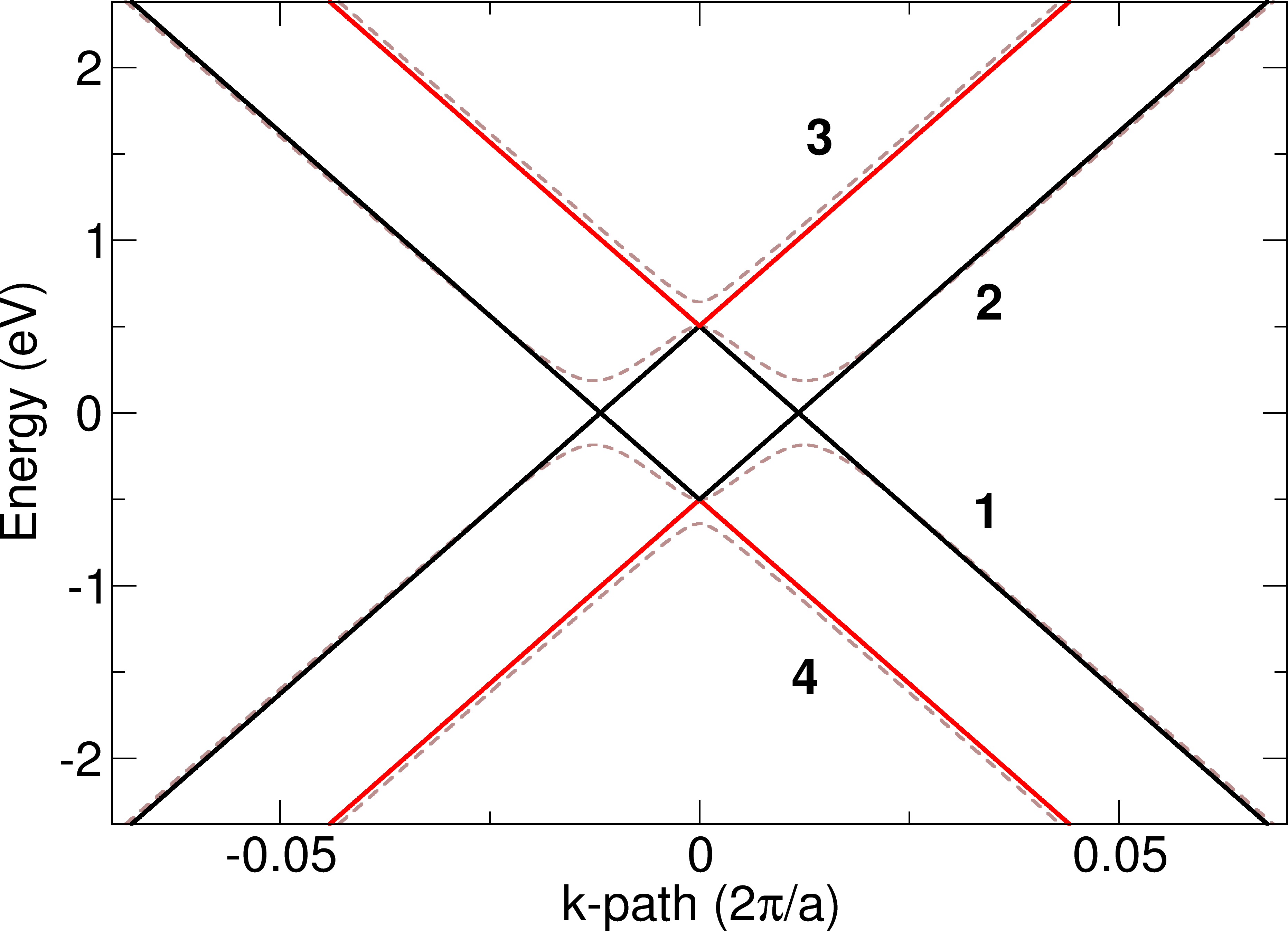
Analytical calculation of the Berry curvature of Eq. (6) would, for an arbitrary stacking, represent a formidable task. To simplify this we break the full Hamiltonian into two sub-systems: a low energy sector spanned by the single layer states labeled 1 and 2 in Fig. 1 and a high energy sector spanned by states 3 and 4. The two basis sets are therefore
| (7) |
for the low energy sector, and
| (8) |
for the high energy sector. In these expressions is the polar angle of the momentum. The justification for decomposing the full Hamiltonian in this way is that the Berry curvature will be associated with those parts of momentum space that, when the interlayer interaction is tuned to zero, have degenerate states. This is the physics captured by the low energy sector described by states 1 and 2. In calculating the Berry curvature for AB and BA stacking Zhang et al.zhang_valley_2013 employed an alternative basis of states 1 and 4, calculating the Berry curvature deep in the valence band. We find that for the case of a general stacking this leads to an erroneous AA contribution to the topological invariant; apparently for the more general case a careful treatment of the low energy bands becomes important. As we will show, our result reproduces as a limit those of Ref. zhang_valley_2013, .
The low energy Hamiltonian in the basis of states 1 and 2 is
| (9) |
while the high energy Hamiltonian in the basis of states 3 and 4 is
| (10) |
where the off-diagonal elements are given by
| (11) |
The eigenvalues of these Hamiltonians are given by
| (12) |
and
| (13) |
with the eigenvectors given by
| (14) |
and
| (15) |
From these we can then reconstruct the wave functions in the original layer-sublattice space and , and then determine the Berry connection , finding
| (16) |
for the low energy sector and
| (17) |
for the high energy sector, where . We must now sum over occupied states and to give
| (18) |
In the limit of large momentum, we can neglect in the above expression and both and reduce to , so thus the bracketed term vanishes. After integrating around a fixed path, we arrive at an expression for the Chern number given by
| (19) |
which depends only on the valley index and the winding number of , Eq. (11). Expressing the generally complex potentials and as their absolute value and phase, the equation for can be written in polar coordinates in the complex plane as
| (21) | |||||
and we see that if , the ellipse turns counter clockwise and the winding number is plus one while if , the relative signs of the sine and cosine terms are different, and the winding number is minus one. The Chern number for arbitrary stacking is therefore
| (22) |
where the potentials and are related to the stacking through Eq. (4). Evidently, this result reduces to the correct form of the Chern index for AB (0 and 2 for the K and K’ valleys respectivey) and BA (2 and 0 for the K and K’ valleys respectively) derived in Ref. zhang_valley_2013, .
IV Metallic lines in the stacking phase diagram
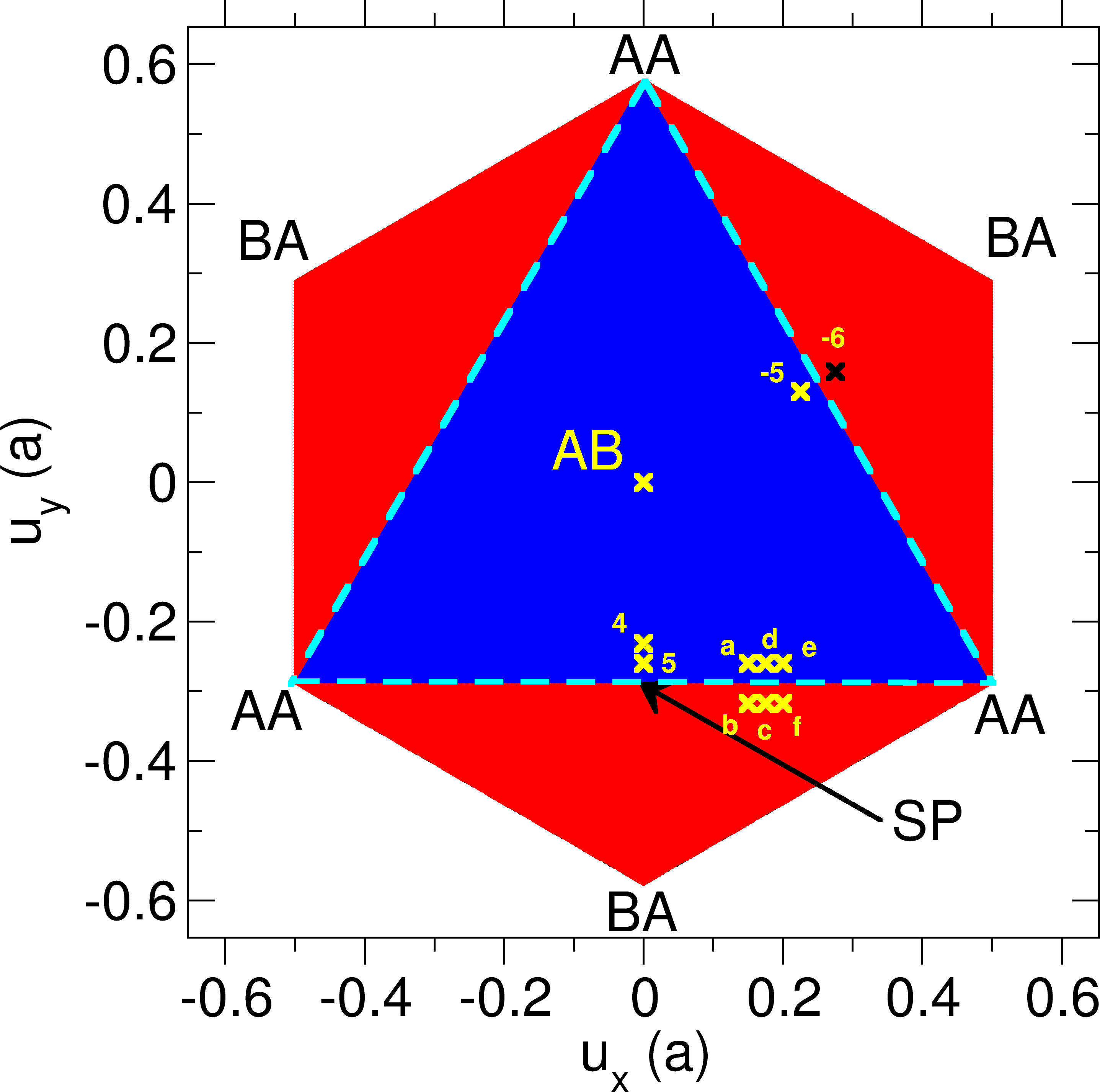
The phase diagram of winding number versus stacking vector is shown in Fig. 2. In principle one can move through this phase diagram by sliding two layers of graphene and so cross a boundary separating distinct topological invariants. On such a boundary the gap must close irrespective of the magnitude of the interlayer potential. To see that the lines separating regions of distinct topological invariants indeed correspond to “permanent metal lines” we calculate the band gap using the low energy Hamiltonian. The eigenvalues of this Hamiltonian are
| (23) |
and so the gap minimum is at , and can only vanish on this circle for
| (24) |
Rewriting the potentials in polar form implies
| (25) |
and so for the band gap to vanish at some momentum angle a necessary and sufficient condition is thus that two potentials have the same magnitude, . The two complex numbers on either side of the equality are then identical for , from which follows. To determine which stacking vectors this corresponds to, we employ the stacking potentials in the first star approximation which from Eq. (4) are found to be
| (26) | ||||
| (27) |
and insertion of these potentials in Eq. (25) then yields
| (28) | ||||
| (29) |
with . This corresponds precisely to the three lines on which the winding number changes sign.
V Numerical method
In order to probe both the veracity and consequences of the general relation between topological index and stacking order, Eq. (22), we now turn to numerical calculations. In what follows we describe our methodology for both electronic structure simulation and atomic relaxation.
V.1 Electronic structure calculations
We model the interlayer displacement field between the regions with stacking vectors by
| (30) |
that depends on three parameters; the location of the boundary , its width and the length of the unit unit cell . As we employ periodic boundary conditions, we require two domain boundaries which we locate at and . For our tight-binding calculations we employ a -band only approximation and take the in-plane and interlayer hopping functions to be parameterized by the same Gaussian form
| (31) |
with and are chosen to give an in-plane nearest neighbor hopping of 2.8 eV and the interlayer and chosen such that the hopping between nearest interlayer neighbours in the AB structure is 0.4 eV. The magnitude of determines how fast the interlayer interaction decays.
For numerical work we do not need to enforce a restriction to linear momentum (Dirac-Weyl approximation) and instead use a Hamiltonian in which the layer diagonal blocks are the full tight-binding description, with the layer off-diagonal blocks treated through Eq. (4):
| (32) |
It is numerically efficient to use a basis of single layer eigenstates, determined from the layer diagonal blocks asfleischmann_perfect_2020
| (33) |
We find a basis size of 1600 of the lowest energy states from each layer provides good convergence for the low energy electronic structure of Eq. (32). In this basis the matrix elements of Eq. (32) are given by
| (34) |
V.2 Lattice relaxation
To calculate atomic relaxation we employ the GAFF force field GAFF for the C–C interactions within the graphene layers and the registry-dependent interlayer potential of Kolmogorov-Crespi KC2005 using our own implementationbutz14 ; fleischmann_perfect_2020 . For the ideal AB-stacked graphene bilayer this calculational setup results in an equilibrium lattice constant of Å and an interlayer distance of Å. Shifting the graphene layers to AA stacking increases the layer separation to Å ( as compared to AB stacking). The AA-stacked bilayer has a higher energy of 4.4 meV per atom as compared to AB-stacking, corresponding to a stacking fault energy of mJ/m2. In SP stacking order (see Fig. 2) the equilibrium distance of the graphene layers and the stacking fault energy are Å (+0.020 Å) and mJ/m2 (0.6 meV per atom), respectively, in excellent agreement with ACFDT-RPA calculations of Srolovitz et al. sor15 .
VI Probing the phase diagram
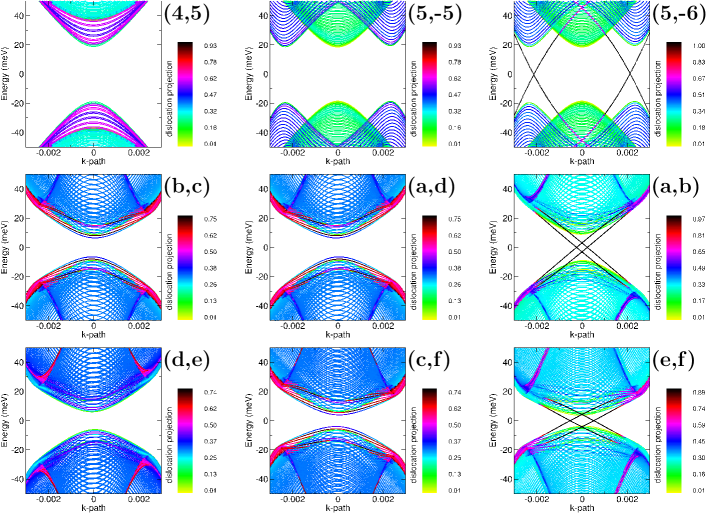
We consider a model system consisting a periodic unit cell with domain walls at and separating regions of stacking in the sequence . By choosing and to have either the same or different valley Chern numbers according to the phase diagram of Fig. 2, a robust test of the relation between valley Chern number and stacking vector can be performed. In Fig. 3 we show band structures that result from choosing in this way. The corresponding stacking vectors for each panel can be read off from the panel label and, as may be observed, in each case where fall either side of a metal line gapless states are found in the spectrum.
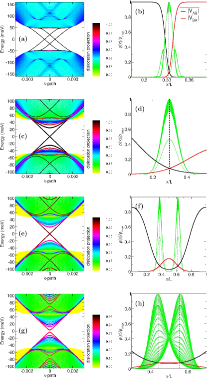
As a further numerical test, we probe the occurrence of bound states at nodes of the function , in systems with smoothly modulated stacking potentials. We consider a unit cell in which we have two partial dislocations at and separating regions of AB and BA stacking; the stacking sequence through the unit cell is thus ABBAAB, with the domain walls characterized by the partial Burgers vectors and . A smooth stacking variation can then be obtained simply by allowing the partial width to become comparable to . In Fig. 4 we see the band structures (left column) and squared wave functions and interlayer potentials (right column) for dislocation widths of (a realistic patial dislocation width), and , and . For the systems shown here we have taken , a fast decaying potential. This implies that for the misregistry of the layers seen within the core of partial dislocation a weak interlayer interaction, as for hopping vectors much greater in length than the minimal interlayer nearest neighbour separation the hopping matrix element quickly falls to zero. This is the reason for the overall weaker interaction seen at the centre of the cell. While this decay is significantly faster than in bilayer graphene (the tight-binding fitting of Ref. lee_zero-line_2016, corresponds to ) it generates the crossing of AB and BA potentials that we require for a numerical test of Eq. (22).
As can be seen from Fig. 4, as the sharp ABBAAB transition of the partial dislocation is broadened to a smooth modulation, an increasing number of states appear in the gap, which is almost closed for the system. However, for each system there are two crossing points of the stacking potentials and and at each, as predicted by the change in topological index, bound states are seen in the right hand panel. (Note that to clearly associate the bound state with the crossing of and in panels (b), (d), and (h), we show a restricted view of a single crossing point.) For the domain wall two right moving and two left moving linear gapless states very similar to those reported in the literaturelee_zero-line_2016 can be seen; this is expected from bulk boundary correspondence as the difference in Chern number across the boundary is 2. As the dislocation broadens the gap fills with an increasing number of additional states. In each case, however, exactly at the crossing points of bound states are observed, fulfilling the expectation of Eq. (22). Note that all states in the gap of the pristine bilayer (100 meV) are shown in right hand panels, which accounts for the large number of states in each panel.
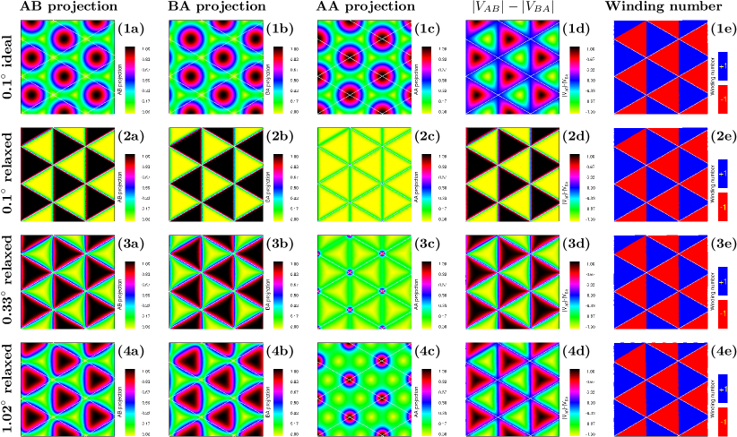
VII A Chern index map of the twist bilayer
Having numerically tested the veracity of the relation between valley Chern number and stacking vector, we now address the question as to how the spatial variation of the valley Chern index is impacted by lattice relaxation in minimally twisted bilayer graphene. For the ideal twist bilayer (row 1, ) the stacking potentials show an equal weight of AB, BA and AA stacking types in the system (as they would for any three stacking projections which would produce a very similar picture but with potential maxima shifted off the high symmetry positions). Upon lattice relaxation this potential landscape dramatically alters: in row 2 we see that the AA potential has all but vanished, remaining only weakly visible at the dislocation core and nodes, with the AB and BA potentials describing a mosaic tiling with symmetry. Increasing the twist angle smooths the edges of this mosaic, and increases strength of the AA potential contribution, see row 3 () and row 4 (). The 4th and 5th columns of this figure display the difference , and the winding number . Remarkably, we see that the spatial variation of the winding number is identical for all systems. From the results of Secs. III and VI, this indicates that the formation of valley-momentum helical states, which is driven by the changing valley Chern number, will be impacted only in details by lattice relaxation.
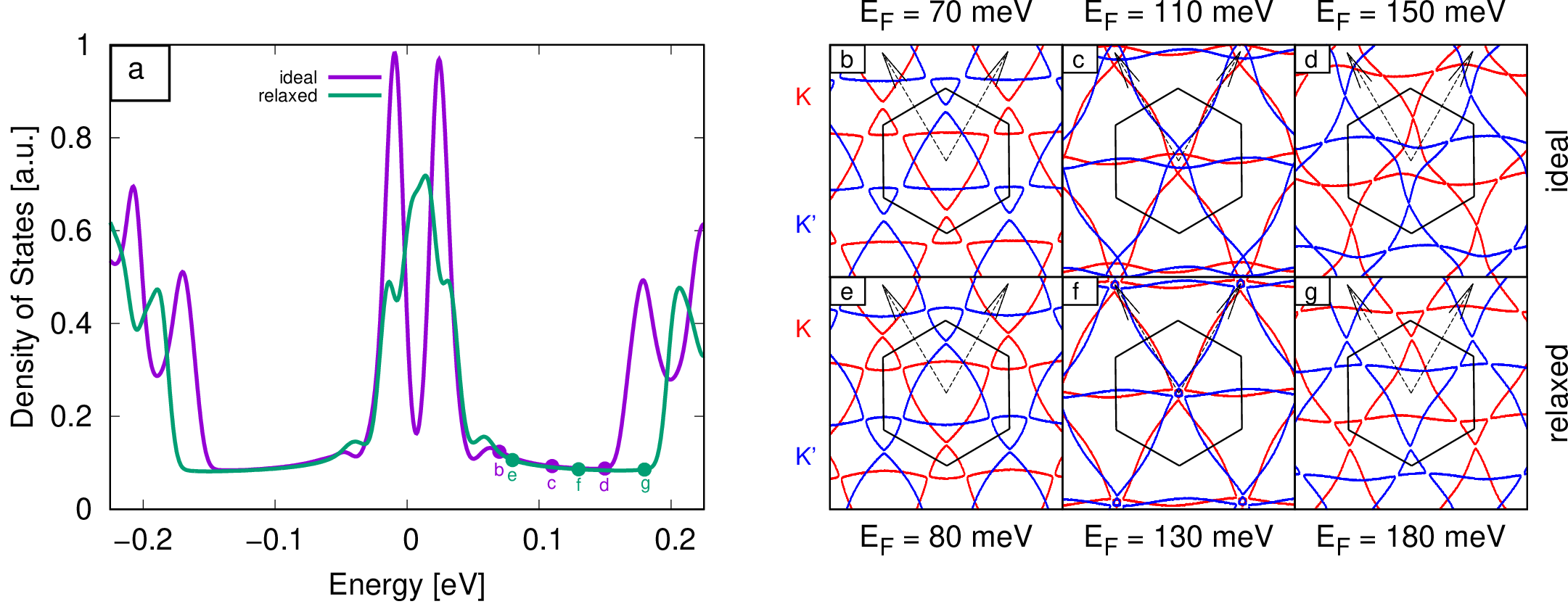
To examine this we show in Fig. 6 the density of states and Fermi surfaces for a twist bilayer of ( in the notation of Ref. shall13, ). While the density of states shows pronounced changes close to the Dirac point, the “valley” between the Dirac point peak and the two shoulder peaks remain largely unchanged. This low, almost constant DOS in the valley region corresponds to the gapless topological states, and as can be seen from the Fermi surfaces, Fig. 6b, the details of this band structure remain qualitatively the same, with some increased hybridization due to relaxation opening the intersection points of the nested Fermi surface (particularly seen in panel Fig. 6g).
VIII Discussion
We have provided a general relation between the topological invariant of bilayer graphene and the stacking vector that describes mutual translation of the layers. We find that the Chern index is given by , with and the AB and BA components of the interlayer stacking potential. This generalizes the well known result that AB and BA stacked bilayer graphene have valley Chern numbers of 0 and 2 (for the K and K’ valley) and 2 and 0 respectively. A consequence of this generalization is that the valley Chern number is now associated with a condition on the interlayer fields rather than the fixed AB and BA structures, and this allows consideration of the occurrence of topologically protected states in regions of smooth stacking variation, such as moirés. As a numerical test of this we have performed simulations of artificially broadened domain walls finding bound states at the crossing of the and , as would be expected due to the change in value of at this point.
With this tool in hand we have examined the valley Chern number for minimally twisted bilayer graphene, finding that the underlying spatial dependence of the valley Chern index is, essentially, independent of atomic relaxation. The topological physics of this material, in particular helical network states, is thus qualitatively similar in the ideal and relaxed twist bilayer. In fact, the ideal twist geometry can be expected to have a much “cleaner” manifestation of the helical network due to the reduced scattering as the interlayer interaction contains only three (first star) momentum boosts, as opposed to the continuum of momentum boosts of the dislocation network.
Acknowledgments
The work was carried out in the framework of the SFB 953 “Synthetic Carbon Allotropes” (project number 182849149) of the Deutsche Forschungsgemeinschaft (DFG). F.W. thanks the Graduate School GRK 2423 (DFG, project number 377472739) for financial support. S.S. and S.S. acknowledge the funding of the DFG, reference SH 498/4-1.
References
- (1) Shuyang Dai, Yang Xiang, and David J. Srolovitz. Twisted Bilayer Graphene: Moiré with a Twist. Nano Letters, 16(9):5923–5927, September 2016.
- (2) Sandeep K Jain, Vladimir Juričić, and Gerard T Barkema. Structure of twisted and buckled bilayer graphene. 2D Materials, 4(1):015018, November 2016.
- (3) Hyobin Yoo, Rebecca Engelke, Stephen Carr, Shiang Fang, Kuan Zhang, Paul Cazeaux, Suk Hyun Sung, Robert Hovden, Adam W. Tsen, Takashi Taniguchi, Kenji Watanabe, Gyu-Chul Yi, Miyoung Kim, Mitchell Luskin, Ellad B. Tadmor, Efthimios Kaxiras, and Philip Kim. Atomic and electronic reconstruction at the van der Waals interface in twisted bilayer graphene. Nature Materials, 18(5):448, May 2019.
- (4) Fernando Gargiulo and Oleg V. Yazyev. Structural and electronic transformation in low-angle twisted bilayer graphene. 2D Materials, 5(1):015019, November 2017.
- (5) Nguyen N. T. Nam and Mikito Koshino. Lattice relaxation and energy band modulation in twisted bilayer graphene. Phys. Rev. B, 96(7):075311, August 2017.
- (6) Jonathan S. Alden, Adam W. Tsen, Pinshane Y. Huang, Robert Hovden, Lola Brown, Jiwoong Park, David A. Muller, and Paul L. McEuen. Strain solitons and topological defects in bilayer graphene. Proceedings of the National Academy of Sciences, 110(28):11256–11260, 2013.
- (7) B. Butz, C. Dolle, F. Niekiel, K. Weber, D. Waldmann, H. B. Weber, B. Meyer, and E. Spiecker. Dislocations in bilayer graphene. Nature, 505(7484):533–7, 2014.
- (8) S. Shallcross, S. Sharma, E. Kandelaki, and O. A. Pankratov. Electronic structure of turbostratic graphene. Phys. Rev. B, 81:165105, 2010.
- (9) S. Shallcross, S. Sharma, and O. Pankratov. Emergent momentum scale, localization, and van Hove singularities in the graphene twist bilayer. Phys. Rev. B, 87:245403, Jun 2013.
- (10) G. Trambly de Laissardière, D. Mayou, and L. Magaud. Localization of dirac electrons in rotated graphene bilayers. Nano Letters, 10(3):804–808, 2010.
- (11) R. Bistritzer and A. H. MacDonald. Moire bands in twisted double-layer graphene. Proc. Natl. Acad. Sci. U.S.A., 108:12233–12237, July 2011.
- (12) D. Weckbecker, S. Shallcross, M. Fleischmann, N. Ray, S. Sharma, and O. Pankratov. Low-energy theory for the graphene twist bilayer. Phys. Rev. B, 93:035452, Jan 2016.
- (13) Pablo San-Jose and Elsa Prada. Helical networks in twisted bilayer graphene under interlayer bias. Physical Review B, 88(12):121408, September 2013.
- (14) Procolo Lucignano, Dario Alfè, Vittorio Cataudella, Domenico Ninno, and Giovanni Cantele. Crucial role of atomic corrugation on the flat bands and energy gaps of twisted bilayer graphene at the magic angle . Physical Review B, 99(19):195419, May 2019.
- (15) M. Angeli, D. Mandelli, A. Valli, A. Amaricci, M. Capone, E. Tosatti, and M. Fabrizio. Emergent symmetry in fully relaxed magic-angle twisted bilayer graphene. Physical Review B, 98(23):235137, December 2018.
- (16) Shengqiang Huang, Kyounghwan Kim, Dmitry K. Efimkin, Timothy Lovorn, Takashi Taniguchi, Kenji Watanabe, Allan H. MacDonald, Emanuel Tutuc, and Brian J. LeRoy. Topologically Protected Helical States in Minimally Twisted Bilayer Graphene. Phys. Rev. Lett., 121(3):037702, July 2018.
- (17) Peter Rickhaus, John Wallbank, Sergey Slizovskiy, Riccardo Pisoni, Hiske Overweg, Yongjin Lee, Marius Eich, Ming-Hao Liu, Kenji Watanabe, Takashi Taniguchi, Thomas Ihn, and Klaus Ensslin. Transport Through a Network of Topological Channels in Twisted Bilayer Graphene. Nano Letters, 18(11):6725–6730, November 2018.
- (18) Maximilian Fleischmann, Reena Gupta, Florian Wullschläger, Simon Theil, Dominik Weckbecker, Velimir Meded, Sangeeta Sharma, Bernd Meyer, and Samuel Shallcross. Perfect and Controllable Nesting in Minimally Twisted Bilayer Graphene. Nano Letters, 20(2):971–978, February 2020.
- (19) C. De Beule, F. Dominguez, and P. Recher. Aharonov-bohm oscillations in twisted bilayer graphene. arXiv:2005.05352, 2020.
- (20) F. Rost, R. Gupta, M. Fleischmann, D. Weckbecker, N. Ray, J. Olivares, M. Vogl, S. Sharma, O. Pankratov, and S. Shallcross. Nonperturbative theory of effective Hamiltonians for deformations in two-dimensional materials: Moiré systems and dislocations. Phys. Rev. B, 100:035101, Jul 2019.
- (21) Ferdinand Kisslinger, Christian Ott, Christian Heide, Erik Kampert, Benjamin Butz, Erdmann Spiecker, Sam Shallcross, and Heiko B. Weber. Linear magnetoresistance in mosaic-like bilayer graphene. Nature Physics, 11:650–653, 2015.
- (22) S. Shallcross, S. Sharma, and H. B. Weber. Anomalous dirac point transport due to extended defects in bilayer graphene. Nature Communications, 8(1):342, 2017.
- (23) D. Weckbecker, R. Gupta, F. Rost, S. Sharma, and S. Shallcross. Dislocation and node states in bilayer graphene systems. Phys. Rev. B, 99:195405, May 2019.
- (24) R. Gupta, F. Rost, M. Fleischmann, S. Sharma, and S. Shallcross. Straintronics beyond homogeneous deformation. Phys. Rev. B, 99:125407, Mar 2019.
- (25) R. Gupta, S. Maisel, F. Rost, D. Weckbecker, M. Fleischmann, H. Soni, S. Sharma, A. Görling, and S. Shallcross. Deformation induced pseudomagnetic fields in complex carbon architectures. Phys. Rev. B, 100:085135, Aug 2019.
- (26) Fan Zhang, Allan H. MacDonald, and Eugene J. Mele. Valley Chern numbers and boundary modes in gapped bilayer graphene. Proceedings of the National Academy of Sciences, 110(26):10546–10551, June 2013.
- (27) Junmei Wang, Romain M. Wolf, James W. Caldwell, Peter A. Kollman, and David A. Case. Development and testing of a general amber force field. Journal of Computational Chemistry, 25(9):1157–1174, 2004.
- (28) Aleksey N. Kolmogorov and Vincent H. Crespi. Registry-dependent interlayer potential for graphitic systems. Phys. Rev. B, 71:235415, Jun 2005.
- (29) Songsong Zhou, Jian Han, Shuyang Dai, Jianwei Sun, and David J. Srolovitz. van der waals bilayer energetics: Generalized stacking-fault energy of graphene, boron nitride, and graphene/boron nitride bilayers. Phys. Rev. B, 92:155438, Oct 2015.
- (30) Changhee Lee, Gunn Kim, Jeil Jung, and Hongki Min. Zero-line modes at stacking faulted domain walls in multilayer graphene. Phys. Rev. B, 94(12):125438, September 2016.