Electrically Controlled Two-Dimensional Electron-Hole Fluids
Abstract
We study the electronic properties of dual-gated electron-hole bilayers in which the two layers are separated by a perfectly opaque tunnel barrier. Combining an electrostatic and thermodynamic analysis with mean-field theory estimates of interacting system chemical potentials, we explain the dependence of the electron and hole densities on the two gate voltages. Because chemical potential jumps occur for both electrons and holes at neutrality, there is a finite area in gate voltage parameter space over which electron and hole densities are equal. In that regime the electron-hole pair density depends only on the sum of the two gate voltages. We are able to explain a recent experimental study of electrically controlled bilayers by allowing for interlayer tunneling and using a non-equilibrium steady-state transport picture.
I Introduction
Recent progress Wang et al. (2019); Rivera et al. (2015, 2016); Mak and Shan (2016); Kim et al. (2017); Burg et al. (2018); Wang et al. (2018); Jauregui et al. (2019); Ciarrocchi et al. (2019); Tran et al. (2019); Jin et al. (2019); Seyler et al. (2019); Regan et al. (2020); Tang et al. (2020) in fabricating and processing two-dimensional (2D) semiconductor multilayers has opened up new opportunities to realize and study the properties of 2D electron-hole systems. Provided that the tunneling between layers is negligible, a bias voltage applied to a bilayer with a spatially indirect band gap, like the one in Fig. 1, simply adjusts the effective band gap. Above a threshold bias voltage the effective band gap is reduced to zero so that electrons are induced in the conduction band of one 2D semiconductor layer, and holes in the valence band of the adjacent layer. In the limit of low electron and hole densities, a regime of bias and gate voltages exists in which the electrons and holes pair into excitonic bound states, and separate electrical contacts can then be used to adjust the exciton chemical potential Xie and MacDonald (2018). In the general case, however, the electron and hole densities are unequal, allowing unprecedented access to systems of fermions with attractive mutual interactions, whose densities are unbalanced Tiene et al. (2020); Subası et al. (2010); Parish et al. (2011); Varley and Lee (2016). In this Article we outline a rigorous framework that relates the dependence of electron and hole densities in the semiconductor bilayers on bias and gate voltages to thermodynamic properties of the interacting electron-hole fluid, focusing first on the case of perfectly opaque barriers between the active layers and then discussing transport and electronic properties in the case where charge leakage between layers plays an important role.
Our paper is organized as follows. Section II presents a formal analysis of the perfect barrier limit in terms of relevant thermodynamic properties of the interacting electron-hole fluid. In Section III we use a mean-field theory of the electron-hole fluid to obtain some concrete but approximate results which illustrate important key qualitative features, in particular the consequences of the singularities that electron-hole pairing produces in thermodynamic properties. In Section IV we combine the results from the previous two sections and show how the carrier densities in the two layers are controlled by the gate voltages. We find that there is a finite area region in the gate-control parameter space where the electron and hole densities are exactly equal, which is especially interesting for the study of exciton physics. Section V generalizes the analysis to the case of non-zero leakage currents and provides an explanation for the transport characteristics observed in a recent experiment Wang et al. (2019). Finally in Section VI we conclude with a discussion of the prospects for realizing new physics in these systems.
II Dual Gated Electron-Hole Fluids
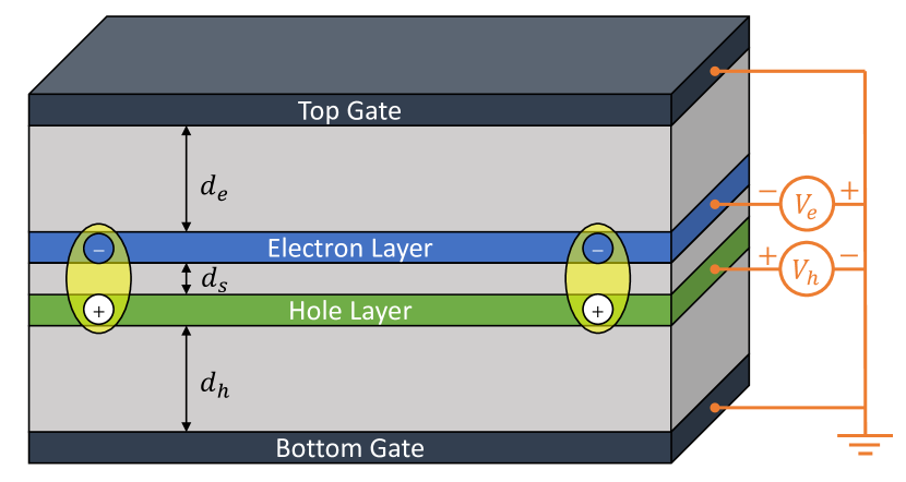
We assume a dual gated structure like that illustrated in Fig. 1. For definiteness we will focus on the case in which the two gates are physically identical and held at the same voltage. We choose the Fermi energy of the gates as the zero of energy, and also set the zero of the electric potential at the gate planes. We assume that the voltages on the contacts to the electron and hole layers, and , can be varied at will, and that no current can flow between layers. Under that circumstance the contacts on the two layers act like reservoirs whose voltages fix the electrochemial potentials of the electrons in those layers. We also assume that and so that the large voltages populate the conduction band in the electron layer and the valence band in the hole layer, allowing us to disregard the remote band degrees of freedom in both layers.
Starting from neutrality and increasing , the electron layer begins to charge when reaches the threshold voltage at which its electrochemical potential reaches the bottom of the conduction band , whereas the hole layer begins to charge when its electrochemical potential reaches the top of the valence band, . We focus on the regime in which both layers are charged, which we refer to as the p-n regime. Applying the Poisson equation we obtain the following relationship between the electric potentials and and the free carrier densities and in the electron and hole layers:
| (1) |
where and are the distances from top and bottom gates to the electron and hole layers, and is the spacing between electron and hole layers. Note that we have absorbed a factor of electron charge in the definition of and so that they have units of energy. The inverse of this linear relationship is
| (2) |
Assuming that , as is typical in experiment Wang et al. (2019), we see that and will typically be nearly equal in magnitude, i.e. that this gating geometry favors nearly balanced electron-hole fluids but allows for large values of the individual layer densities:
| (3) |
Due to the small interlayer distance, the electric field between the two layers is typically much larger than the electric field between the active layers and the gates.
The dependence of the carrier densities on the bias voltages applied to the active layers is determined by the following pair of non-linear equations:
| (4) |
Note that and in these equations refer to the conduction and valence band edges in the absence of carriers and are defined relative to the Fermi level of the gates. The left-hand sides of these equations are functions of and with and given by the electrostatic equations (2), and and determined by the many-body physics of the electron-hole fluid. In Eq. (4) and are defined as the electrochemical potentials of the electron and hole layers relative to their local band extrema. Experiments which measure and as a function of and therefore provide a valuable thermodynamic probe of electron-hole fluid properties. In the following section we discuss mean-field theory estimates for and that provide valuable insight into expected properties. In general Eqs. 4 define two lines in space that intersect at the equilibrium carrier densities. As we discuss below, however, singularities along the line associated with the formation of excitonic bound states require special considerations.
III Mean-Field Theory of the Unbalanced Electron-Hole Fluid
We consider a bilayer electron-hole system with electron and hole densities and , neutralizing backgrounds in both electron and hole layers, and the band extrema energies of both the conduction band and the valence band set to zero. With these conventions, the electron and hole chemical potentials of the interacting electron-hole system correspond to the chemical potentials and in Eqs. (4). The mean-field Hartree-Fock Hamiltonian of the electron-hole system is
| (5) |
where is the two-band single-particle Hamiltonian for electrons and holes
| (6) |
where stand for the conduction band of the electron layer and the valence band of the hole layer. As explained above, the zero of energy for the electron layer is chosen at the bottom of the conduction band, and for the hole layer at the top of the valence band. Because of the assumption of neutralizing backgrounds there is no electrostatic mean-field potential, and is the exchange self-energy:
| (7) |
where is the area of the two-dimensional system, is the band index, is the intralayer Coulomb interaction, is the interlayer Coulomb interaction at interlayer distance , and is the dielectric constant of the surrounding three-dimensional material. In Eq. (7) is the density matrix calculated relative to the density matrix when the conduction band is empty and the valence band is full:
| (8) |
Below we express lengths and energies in terms of characteristic scales and , where is the reduced effective mass. For simplicity we perform numerical calculations only for the case. This model approximates MoSe2/WSe2 bilayers surrounded by hexagonal boron nitride (hBN) dielectrics if we choose , and , which implies that and . The calculations below are for the case , corresponding approximately to the case with one or two hBN layers between the MoSe2 and WSe2 monolayers.
In order to provide an interpretation for the mean-field theory results presented below, we first discuss a simple phenomenological picture in which we assume that the electron-hole fluid consists of paired (excitons) and unpaired electrons or holes. If we assume that the physically preferred state of the system is one with the maximum number of electron-hole pairs, then the system consists of excitons and unpaired electrons or holes. In this picture the total energy per area of the system at small and can be approximated by the simple expression
| (9) |
where is the exciton binding energy, describes exciton-exciton interactions, and is the inverse thermodynamic density-of-states of the unpaired electrons or holes. This expression implies that the total energy has a cusp at . The chemical potentials in which we are primarily interested are given by
| (10) |
For adding an electron adds an exciton and removes a free carrier whereas for adding an electron simply adds a free carrier. In a similar way adding a hole simply adds a free carrier for , whereas for it adds an exciton and removes a free carrier. For this reason the chemical potentials of electrons and holes jump in opposite directions by when the line is crossed. The chemical potential for excitons
| (11) |
is however continuous. For our ansatz energy expression, Eq. (9), places all electrons and holes into pairs and the exciton chemical potential
| (12) |
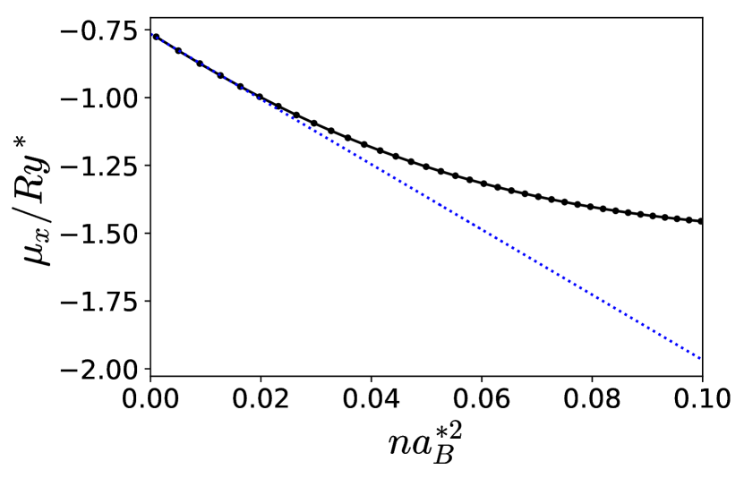
We now compare this simple physical picture with microscopic mean-field theory calculations performed as a function of and . First of all, in Fig. 2(a) we plot the exciton chemical potential at calculated as a function of and compare it with Eq. (12). By linearly fitting the small- part of the curve we find that the exciton binding energy and the exciton-exciton interaction parameter . The negative value of here implies that the interaction between interlayer excitions would be attractive at the considered interlayer separation if electrostatic interactions, which are suppressed at this stage because of the neutralizing backgrounds in each layer in the reference system calculation, were ignored. Technically this property reflects the dominance of intralayer Coulomb interactions, and agrees with previous studies Wu et al. (2015). At large exciton density () higher-order interaction terms come into play, the curve deviates from the linear relation of Eq. 12, and the simple expression (9) is no longer a good approximation.
According to Eq. (9)
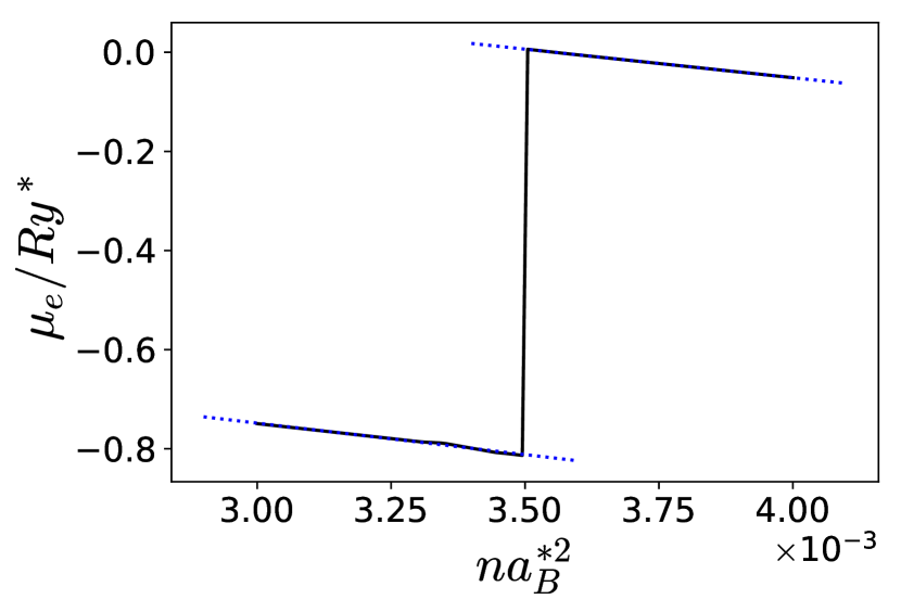
| (13) |
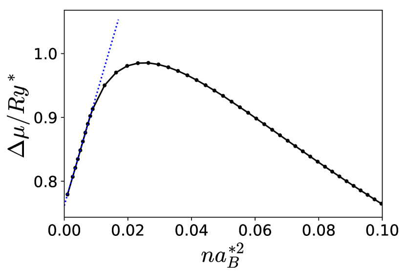
where is the Heaviside step function. The electron chemical potential calculated from microscopic mean-field theory is plotted as a function of for fixed in Fig. 2(b). The upward jump in the electron chemical potential anticipated in the ansatz expressions is prominent. The parameter , the quasiparticle inverse thermodynamic density of states, accounts for the rate of change of electron chemical potential near the point. A linear fit gives . This negative value of is related to the negative compressibility property, which applies also in single-component systems, and is due to the dominance of exchange interactions in low-density electron gases Eisenstein et al. (1992, 1994); Ying et al. (1995). The size of the chemical potential jump at is plotted vs. carrier density in Fig. 2(c). The ansatz expression for this quantity is
| (14) |
However, comparison of Fig. 2(a) and 2(c) shows that the behavior of and are very different when is not small. Fitting these two quantities at the small- part yields different slopes but almost identical intercepts. This implies that while the physical picture represented by Eq. (9) is oversimplified, it does capture a large part of the truth.
The chemical potentials calculated in this section are based on a temperature mean-field theory, which yields an electron-hole pair condensate ground state. Although this theory is expected to become exact at in the limit of very low carrier densities, it is expected to fail at large carrier densities. It is generally thought that Fogler et al. (2014); Perali et al. (2013); Neilson et al. (2014) at high enough carrier density a Mott limit is reached above which exciton condensation does not occur. Although we use these chemical potentials in the following section to discuss some qualitative expectations, an equally important aspect of our analysis is that it can be used in combination with experimental measurements of the dependence of carrier densities on gate voltages to extract chemical potential data from experimental observations. Experiments of this type would be especially valuable at higher temperatures where mean-field theory is not expected to be reliable.
IV Gate Control of Carrier Densities
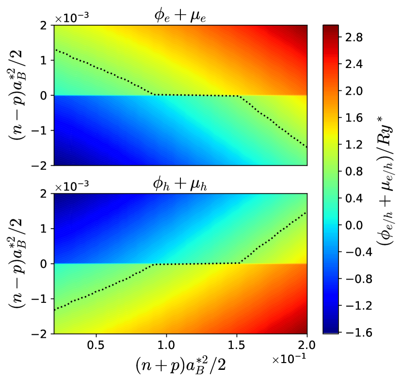
The left-hand sides of Eqs. (4) are functions of and . For given values of and , and are given by the electrostatic equations (2), while and are more complex quantities that depend on correlations in the electron-hole fluid. For given gate voltages and , Eqs. (4) can have one or more solutions, the latter instance would signal bistability or multi-stability of the electron-hole system. In Figs. 3 we plot , calculated using mean-field theory chemical potentials, as functions of total carrier density and total charge density . One important feature of in this plot is the jump in electrochemical potentials across the line discussed above. Aside from the jump at neutrality, increasing net charge density changes the electrochemical potentials rapidly mainly because of the electrostatic contributions. increases with , decreases with , and both changes are rapid because of the relatively large distance to the gates. (Note the difference in scales for the and axes in Figs. 3.) At fixed , both electrochemical potentials increase with , mainly because of band-filling.
From Eqs. (4) we see that the equilibrium values of and for given values of the control gate voltages and correspond to the intersections of the contour lines in Figs. 3 along which and . Since the contour lines of have negative slopes when plotted with along the -axis and along the -axis (as in Figs. 3) while those for have positive slopes, the lines never intersect more than once. We conclude the bistability is unlikely when the electron and hole layers are separated by an hBN tunneling barrier and the gates are well separated from the active layers.
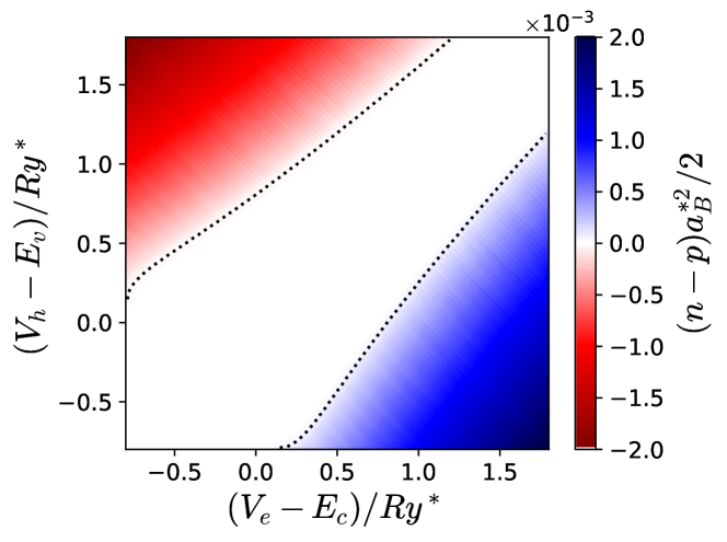
Special care must be taken along the line where the electron and hole electrochemical potentials jump, yielding the horizontal portions of the contour lines in Fig. 3. The electron and hole chemical potentials are ill defined along these horizontal line segments because it is not energetically allowed to exchange particles with individual reservoirs. It is however possible to exchange an electron-hole pair with the reservoirs via a two-particle correlated tunneling process Xie and MacDonald (2018). Correlated electron-hole tunneling is relevant when the difference between and is smaller than the chemical potential jump at neutrality, so that the horizontal segments of two contour lines in Fig. 3 intersect. Under this circumstance the exciton chemical potential is still well defined, and its value at is determined by solving the pair equilibrium condition
| (15) |
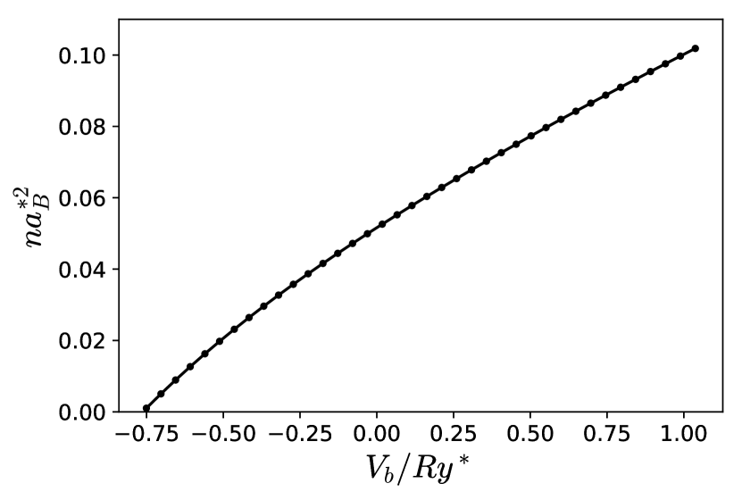
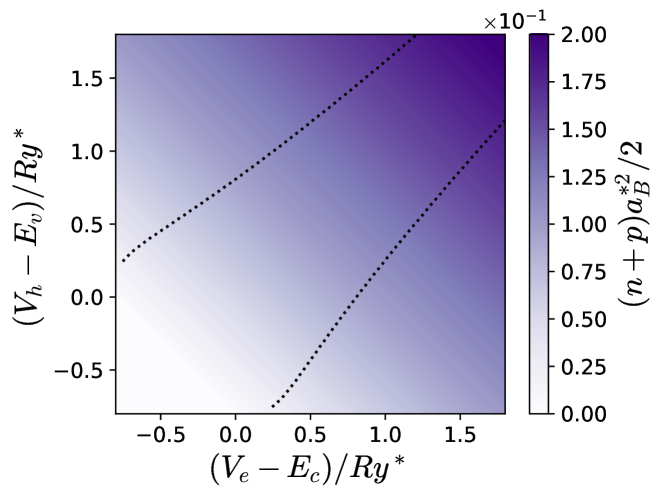
This implies a finite region (rather than a line) in the parameter space in which as illustrated in Fig. 4. The width of this region first increases with increasing gate voltages and then narrows. Defining the right-hand side of Eq. (15) as the bias voltage we obtain the results for the exciton density as a function of shown in Fig. 5. The system is supplied with excitons when . Above the bias voltage threshold the curve is initially linear because of exciton-exciton interactions. The sum of electron and hole densities varies smoothly with gate voltage in the entire plane as illustrated in Fig. 6.
V Leakage Currents
The theory in the previous sections applies when there is no current flowing between layers. In the presence of a tunneling current, the theory still applies as a good approximation if the current is small enough so that we can assume quasi-equilibrium in each layer. In the following we discuss the opposite limit, in which a large leakage current between layers requires a non-equilibrium transport picture. By analyzing this limit we are able to qualitatively explain the transport characteristics observed in a recent experimental study of electrically controlled electron-hole bilayers Wang et al. (2019).
For definiteness we consider MoSe2/WSe2 bilayer systems in which the MoSe2 layer is n-type and the WSe2 is p-type. In a typical experimental setup, the two layers do not perfectly overlap, leaving isolated monolayer regions between the bilayer region and the electrical contacts. We sketch an idealized geometry in Fig. 7 in which we divide the system into three parts: regions I and III are isolated WSe2 and MoSe2 monolayer regions, while region II is the overlapped bilayer region. Assuming that is above threshold, region I is filled with holes with density . Imagine we now increase from a small value. When is below threshold, there are no free carriers in the MoSe2 layer, so no current flows and the electric field distribution is not affected by the MoSe2 layer. The whole WSe2 layer is uniformly charged and in equilibrium with the left lead. The electric potential on the MoSe2 layer in region II is very close to that of the WSe2 layer due to the small interlayer distance, while in region III the electric potential is the same as the gates since the whole layer is neutral. The electric potential jump between regions II and III implies a sharp bending of the MoSe2 bands at the boundary.
When increases above threshold, region III starts to get charged toward electron density . Due to the electric potential jump, current is injected into empty states in region II and tries to fill the band to the same level as in region III. The injection current is a function of (and therefore depends on only). Importantly it does not depend on the physics in regions I and II (as long as region II is far from equilibrium with III). Were it not for the leakage current between the two layers in region II, the whole MoSe2 layer would finally come to equilibrium with the right lead, and the theory in the previous sections would apply. However, as we schematically show in Fig. 7, a large leakage current can prevent the system from establishing equilibrium. The leakage current is a monotonically increasing function of the carrier densities and . If and reach value such that before equilibrium is established, the system will reach a non-equilibrium current-carrying steady state. The current through the system is limited by the injection current from region III, which depends only on . Meanwhile, the WSe2 layer in regions I and II maintains equilibrium with the left lead.
Similar considerations apply to region I, which like region III also has a maximum injection current that is a function of . When is so large that , the tunneling current is limited by the injection current from region I, while regions II and III stay in equilibrium with the right lead. The transition takes place when . Since and are similar functions of carrier density, roughly speaking this happens when , or . The most important conclusion from this analysis above is that, as long as the system is in the p-n regime, the tunneling current is determined by the following equation:
| (16) |
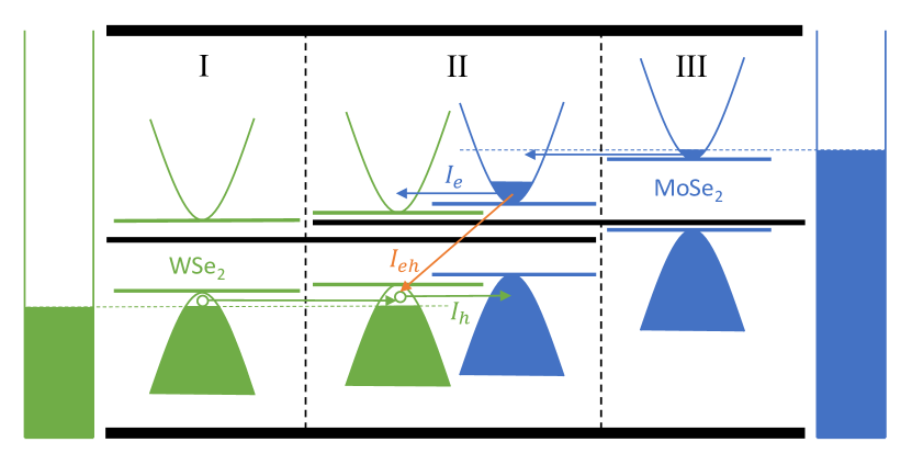
The leakage current consists of three parts (see Fig. 7): electron tunneling , hole tunneling , and interband electron-hole phonon-assisted tunneling or optical recombination . Due to the relatively weak electroluminescence observed in experiments, we assume that . Then the tunneling current has a threshold when the chemical potential in the electron layer is above the bottom of the conduction band in the hole layer (or when the chemical potential in the hole layer is below the top of the valence band in the electron layer). Above threshold the tunneling conductance far exceeds the corresponding injection current conductance from monolayer regions at the same chemical potential. In this case the total current is limited by injection from monolayer regions as discussed above, and the details of the interlayer tunneling process do not matter. One possible way to study interlayer tunneling is to tune the chemical potential below threshold, so that the tunneling current only has a single weak component . This can be made easier by applying a vertical electric field between the two layers to tune the indirect band gap. The dependence of on carrier densities can provide clues that help us understand the correlated electron-hole states and possibly provide evidence for exciton condensation.
We now provide a crude estimate of the injection current by considering the ballistic transport limit. Consider an electron with momentum moving across a rectangular region with length and width . The electron has velocity along , and contributes to current
| (17) |
Assuming that all electrons with contribute to the current, we integrate over half of the Fermi sea (accounting for valley degeneracy) to obtain
| (18) |
Here the Fermi momentum is related to the carrier density by
| (19) |
For the monolayer region, it is a good approximation to assume when because of its large distance from the gates. By simple electrostatics the carrier density is given by
| (20) |
For , and , we obtain . Then for and , from Eq. (18) we estimate the current
| (21) |
which is, as expected, much larger than the current observed in experiment due to the unrealistic assumption of perfect transmission. The ballistic transport picture gives , in contrast to the relation found in experiment. The difference can be explained by the fact that electron transmission is not perfect and depends on energy. We can make our result agree with the experiment by introducing a phenomenological energy-dependent transmission probability where is the electron energy relative to conduction band bottom. With a similar analysis for holes, we restore the cubic law found in experiment Wang et al. (2019):
| (22) |
VI Discussion
In this article we have analyzed how two gate voltages and can be used to control the electron and hole densities and , and hence all properties, of bilayer two-dimensional electron-hole fluids. When there is no leakage current between electron and hole layers contacted by electrodes with different chemical potentials, bias voltages can be used to tune the bilayer into an effective semi-metal regime in which carriers are present in both and layers. Because of jumps in electron and hole chemical potentials related to electron-hole pair bound state formation that occur along the carrier-compensation line, there is a finite area in the gate-control region, instead of a line, within which . In this region the electron and hole chemical potentials are not individually well defined. Instead their sum, identified as the exciton chemical potential, is well defined and controlled by the value of . Fig. 4 outlines the boundaries of the excitonic area in the control space as estimated by mean-field theory. We anticipate that the width of this region, which is a measure of the chemical potential jumps at neutrality - referred to as the exciton binding energy below - narrows with increasing exciton density due to screening Fogler et al. (2014); Perali et al. (2013); Neilson et al. (2014), exciton-exciton attractive van der Waals interactions Lozovik and Berman (1997), and other effects that are not captured by mean-field theory. Although the fate of this quantity, which has not previously been experimentally accessible, is usually not explicitly discussed in the literature, the most common view appears to be that the exciton binding energy drops suddenly to zero at a first-order Mott transition. Another view is that the exciton binding energy declines monotonically with increasing density in a crossover between BEC and BCS limits, but never vanishes. Still another possiblity is that the exciton binding energy vanishes smoothly at a continuous phase transition. Capacitive studies of electron-hole bilayers should be able to provide a definitive experimental answer to this question.
Within the finite-area exciton region of the gate control space acts as a chemical potential for excitons. By using contact pairs to establish exciton reservoirs with different chemical potentials at different locations in a bilayer system, we anticipate that it will be possible to measure electrical and thermal transport properties of excitons, and to design exciton circuits. This exciting prospect is a principle motivation for formulating the analysis in this Article.
We have compared our analysis with a recent paper that reports on important progress toward electrical control of electron-hole bilayers, and therefore of the their optical properties. We conclude that the transport properties reported in Ref. Wang et al., 2019 are indicative of electron-hole systems that are not in a quasi-equilibrium configuration, but instead in a transport steady state that is strongly influenced by the intra-band leakage current between the bilayers. The leakage current is easily reduced, however, by inserting dielectric layers between the 2D semiconductors, or simply by reducing the area of overlap between the two 2D semiconductor layers. We can anticipate that further progress will enable accurate control of quasi-equilibrium electron-hole bilayers, and by staying within the region, electrical and thermal control of exciton currents.
The relationship between electron and hole densities and gate voltages depends on both many-body correlations and disorder within the 2D semiconductor layers. In this paper we have ignored disorder and used a mean-field theory to describe interactions in the electron-hole system. The mean-field theory is expected to be accurate at low electron and hole densities, but it is precisely in this regime that disorder is most important. We expect that future experimental studies of electrically controlled electron-hole bilayers, and future progress controlling disorder, will shed light on both aspects of electron-hole bilayer physics.
VII Acknowledgements
The authors thank Kin Fai Mak and Jie Shan for helpful discussions. This work was supported by the U.S. Department of Energy, Office of Science, Basic Energy Sciences, under Award # DE‐SC0019481 and by Welch Foundation grant TBF1473.
References
- Wang et al. (2019) Z. Wang, D. A. Rhodes, K. Watanabe, T. Taniguchi, J. C. Hone, J. Shan, and K. F. Mak, Evidence of high-temperature exciton condensation in two-dimensional atomic double layers, Nature 574, 76 (2019).
- Rivera et al. (2015) P. Rivera, J. R. Schaibley, A. M. Jones, J. S. Ross, S. Wu, G. Aivazian, P. Klement, K. Seyler, G. Clark, N. J. Ghimire, et al., Observation of long-lived interlayer excitons in monolayer – heterostructures, Nature communications 6, 1 (2015).
- Rivera et al. (2016) P. Rivera, K. L. Seyler, H. Yu, J. R. Schaibley, J. Yan, D. G. Mandrus, W. Yao, and X. Xu, Valley-polarized exciton dynamics in a semiconductor heterostructure, Science 351, 688 (2016).
- Mak and Shan (2016) K. F. Makand J. Shan, Photonics and optoelectronics of semiconductor transition metal dichalcogenides, Nature Photonics 10, 216 (2016).
- Kim et al. (2017) J. Kim, C. Jin, B. Chen, H. Cai, T. Zhao, P. Lee, S. Kahn, K. Watanabe, T. Taniguchi, S. Tongay, et al., Observation of ultralong valley lifetime in heterostructures, Science advances 3, e1700518 (2017).
- Burg et al. (2018) G. W. Burg, N. Prasad, K. Kim, T. Taniguchi, K. Watanabe, A. H. MacDonald, L. F. Register, and E. Tutuc, Strongly enhanced tunneling at total charge neutrality in double-bilayer graphene- heterostructures, Physical review letters 120, 177702 (2018).
- Wang et al. (2018) Z. Wang, Y.-H. Chiu, K. Honz, K. F. Mak, and J. Shan, Electrical tuning of interlayer exciton gases in bilayers, Nano letters 18, 137 (2018).
- Jauregui et al. (2019) L. A. Jauregui, A. Y. Joe, K. Pistunova, D. S. Wild, A. A. High, Y. Zhou, G. Scuri, K. De Greve, A. Sushko, C.-H. Yu, et al., Electrical control of interlayer exciton dynamics in atomically thin heterostructures, Science 366, 870 (2019).
- Ciarrocchi et al. (2019) A. Ciarrocchi, D. Unuchek, A. Avsar, K. Watanabe, T. Taniguchi, and A. Kis, Polarization switching and electrical control of interlayer excitons in two-dimensional van der waals heterostructures, Nature photonics 13, 131 (2019).
- Tran et al. (2019) K. Tran, G. Moody, F. Wu, X. Lu, J. Choi, K. Kim, A. Rai, D. A. Sanchez, J. Quan, A. Singh, et al., Evidence for moiré excitons in van der waals heterostructures, Nature 567, 71 (2019).
- Jin et al. (2019) C. Jin, E. C. Regan, A. Yan, M. I. B. Utama, D. Wang, S. Zhao, Y. Qin, S. Yang, Z. Zheng, S. Shi, et al., Observation of moiré excitons in heterostructure superlattices, Nature 567, 76 (2019).
- Seyler et al. (2019) K. L. Seyler, P. Rivera, H. Yu, N. P. Wilson, E. L. Ray, D. G. Mandrus, J. Yan, W. Yao, and X. Xu, Signatures of moiré-trapped valley excitons in heterobilayers, Nature 567, 66 (2019).
- Regan et al. (2020) E. C. Regan, D. Wang, C. Jin, M. I. B. Utama, B. Gao, X. Wei, S. Zhao, W. Zhao, Z. Zhang, K. Yumigeta, et al., Mott and generalized wigner crystal states in moiré superlattices, Nature 579, 359 (2020).
- Tang et al. (2020) Y. Tang, L. Li, T. Li, Y. Xu, S. Liu, K. Barmak, K. Watanabe, T. Taniguchi, A. H. MacDonald, J. Shan, et al., Simulation of hubbard model physics in moiré superlattices, Nature 579, 353 (2020).
- Xie and MacDonald (2018) M. Xieand A. H. MacDonald, Electrical reservoirs for bilayer excitons, Physical review letters 121, 067702 (2018).
- Tiene et al. (2020) A. Tiene, J. Levinsen, M. Parish, A. MacDonald, J. Keeling, and F. Marchetti, Extremely imbalanced two-dimensional electron-hole-photon systems, Physical Review Research 2, 023089 (2020).
- Subası et al. (2010) A. Subası, P. Pieri, G. Senatore, and B. Tanatar, Stability of sarma phases in density imbalanced electron-hole bilayer systems, Physical Review B 81, 075436 (2010).
- Parish et al. (2011) M. M. Parish, F. M. Marchetti, and P. B. Littlewood, Supersolidity in electron-hole bilayers with a large density imbalance, EPL (Europhysics Letters) 95, 27007 (2011).
- Varley and Lee (2016) J. Varleyand D. Lee, Structure of exciton condensates in imbalanced electron-hole bilayers, Physical Review B 94, 174519 (2016).
- Wu et al. (2015) F.-C. Wu, F. Xue, and A. H. MacDonald, Theory of two-dimensional spatially indirect equilibrium exciton condensates, Physical Review B 92, 165121 (2015).
- Eisenstein et al. (1992) J. Eisenstein, L. Pfeiffer, and K. West, Negative compressibility of interacting two-dimensional electron and quasiparticle gases, Physical review letters 68, 674 (1992).
- Eisenstein et al. (1994) J. Eisenstein, L. Pfeiffer, and K. West, Compressibility of the two-dimensional electron gas: Measurements of the zero-field exchange energy and fractional quantum hall gap, Physical Review B 50, 1760 (1994).
- Ying et al. (1995) X. Ying, S. Parihar, H. Manoharan, and M. Shayegan, Quantitative determination of many-body-induced interlayer charge transfer in bilayer electron systems via shubnikov–de haas measurements, Physical Review B 52, R11611 (1995).
- Fogler et al. (2014) M. Fogler, L. Butov, and K. Novoselov, High-temperature superfluidity with indirect excitons in van der waals heterostructures, Nature communications 5, 1 (2014).
- Perali et al. (2013) A. Perali, D. Neilson, and A. R. Hamilton, High-temperature superfluidity in double-bilayer graphene, Physical review letters 110, 146803 (2013).
- Neilson et al. (2014) D. Neilson, A. Perali, and A. Hamilton, Excitonic superfluidity and screening in electron-hole bilayer systems, Physical Review B 89, 060502 (2014).
- Lozovik and Berman (1997) Y. E. Lozovikand O. Berman, Phase transitions in a system of spatially separated electrons and holes, Journal of Experimental and Theoretical Physics 84, 1027 (1997).