Corresponding author: hadar@phys.huji.ac.il
Quantum-Dot Assisted Spectroscopy of Degeneracy-Lifted Landau Levels in Graphene
Abstract
Energy spectroscopy of strongly interacting phases requires probes which minimize screening while retaining spectral resolution and local sensitivity. Here we demonstrate that such probes can be realized using atomic sized quantum dots bound to defects in hexagonal Boron Nitride tunnel barriers, placed at nanometric distance from graphene. With dot energies capacitively tuned by a planar graphite electrode, dot-assisted tunneling becomes highly sensitive to the graphene excitation spectrum. The spectra track the onset of degeneracy lifting with magnetic field at the ground state, and at unoccupied exited states, revealing symmetry-broken gaps which develop steeply with magnetic field - corresponding to Landé factors as high as 160. Measured up to T, spectra exhibit a primary energy split between spin-polarized excited states, and a secondary spin-dependent valley-split. Our results show that defect dots probe the spectra while minimizing local screening, and are thus exceptionally sensitive to interacting states.
Introduction
The use of electron tunneling as a spectroscopic probe for condensed matter systems was first demonstrated by Giaever Giaever_1960 , who applied an oxide tunnel barrier to map the gap in the excitation spectrum of superconductors. Tunneling measurements involve a source electrode which couples to a sample system through a barrier - with the sample density of states (DOS) encoded in the differential change in the tunnel current at a finite source bias Wolf_book . Tunneling became a generic probe, able to address a broad range of conducting samples, following the introduction of the scanning tunneling microscope (STM) Binnig_1982 .
Certain types of samples, however, challenge the existing tunneling methodology. For samples with low DOS, applied bias voltage leads to local charging effects, enhanced by differences in the work functions of the probe and sample. In graphene, for example, voltage applied to a local tunnel probe changes the potential landscape Jung2011 ; Wang_Crommie_2012 ; Zhao_WGM_STM ; Brar_2011 . At finite magnetic fields where graphene DOS becomes sharply peaked at Landau level energies Zhang2005 ; Luican2011 ( being level index), deformation of the potential isolates local regions due to incompressible strips Wang_Crommie_2012 . This is further complicated by the need to reach elevated Landau levels, requiring bias voltages reaching well over 100 mV.
An ideal probe would be local in its physical extent, minimize screening of local interactions and at the same time retain a parallel geometry to avoid non-homogeneous charging. In addition, it should sustain a high bias without deforming local potentials. Here we show that these seemingly contradicting requirements are fulfilled by resonant tunneling through quantum dots (QDs) bound to atomic defects within van der Waals tunnel barriers Greenaway2018 ; Dvir_PRL_2019 . Graphene-based tunnel junctions are highly parallel Mishchenko_2014 , and dot energies are capacitively tuned by the planar electrode, thus avoiding local charging effects due to applied bias. Barrier-embedded dots are nanometric - both in their physical dimensions, and in their proximity to the sample layer. Thus, they are sensitive to regions few nm large. Finally, defect dots lack any degree of freedom for charge rearrangement, they do not screen local interactions, and are hence less invasive than metallic probes.
When QDs couple weakly to the source and drain electrodes, they permit resonant charge transport through sharply peaked energy levels. In this regime, sample DOS is probed by the current through the dot, rather than differential current - avoiding large DC contributions. QDs are utilized as local thermometers Venkatachalam_2012 ; Maradan_2014 , where energy distribution is tracked using the energy-selective nature of injection and ejection of carriers through the QD. Alternatively, by electrostatic tuning of the QD level, sequential tunneling through the QD singles out the sample DOS in resonance with the dot - as seen in the gate-tunable dots used to probe the spectra of superconductor-proximitized nanowires Deng_2016 ; Junger_2019 .
We demonstrate the utility of QD-assisted spectroscopy in a study of the graphene excitation spectrum. In the graphene quantum Hall regime, Landau levels are fourfold degenerate. This SU(4) symmetry allows for several distinct paths of symmetry breaking Alicea_2006 ; Goerbig2006 ; Yang_2006 ; Nomura_2006 ; Kharitonov_2012 ; Fuchs_2007 driven by magnetic field, causing the emergence of ordered ground states which may break either spin or valley degeneracy. The order in which these symmetries should break is subject to debate: While the spin degeneracy is broken by the Zeeman effect, the breaking of valley degeneracy via magnetic field is not as straight-forward. It appears to depend on sample-specific properties such as disorder and the effect of interactions Young2012 . Specifically, and Landau levels differ in wavefunction localization, causing a difference in the energy splitting due to lifting of the valley degeneracy. The magnitudes of the Zeeman effect and the short range interactions compete, resulting in different hierarchies between the spin and valley degeneracy lifting.
So far, existing experiments sensitive to degeneracy lifting effects were provided by probes sensitive to the ground state. These include transport Young2012 ; PhysRevLett.99.106802 ; PhysRevLett.96.136806 and STM measured near the Fermi energy Song2010 ; Li_STM_2019 . The nature of degeneracy lifting in excited states remains an open question: A two-fold splitting of the filled level has been observed by STM Song2010 , and it is indeed clear that excited energy levels should retain the Zeeman splitting. In excited state spectroscopy, carriers are injected into non-populated levels, or ejected from fully populated levels. In this scenario, any deviation from single-particle Zeeman splitting would indicate that energy levels are affected by inter-Landau-level interactions. A non-trivial role of interactions will be manifest in two ways. First, any enhancement of the Landé factor from the non-interacting value, and second, the appearance of valley splitting in full or empty Landau levels.
Results
Defect-Assisted Tunneling at Zero Magnetic Field
In this work we report measurements of defect assisted transport between graphene and graphite separated by a hBN barrier. The barrier-defect energy is tunable by an electric field which originates from a top-gate and penetrates through the graphene layer. We carry out measurements up to magnetic fields of T, and find an intricate pattern of lifting of both valley and spin degeneracies upon injection of carriers to the and excited Landau levels. The spectral splitting is dominated by a strongly enhanced Zeeman term, and valley-split energies are found to exhibit spin-valley coupling.
Defects are regularly found in exfoliated materials, and their signatures have been observed via photoluminescence in transition metal dichalcogenides (TMD) Chakraborty2015 ; He2015 and hexagonal Boron Nitride (hBN) doi:10.1021/acsnano.6b03602 layers. Coupling defect-dots to source and drain electrodes entails placing an insulating layer between two conductors the same geometry used for tunnel junctions stacked using the vdW transfer technique Dvir2018 ; Dvir2018b (Figure 1(a)). This results in single charging behavior characteristic of quantum dots, as seen both in hBN and TMDs Chandni2015 ; Papadopoulos2019 ; Greenaway2018 ; Khanin2019 . The dimension of a dot embedded within barriers depends on the type of defect and dielectric properties of the medium, and can range from the atomic size to a few nm Papadopoulos2019 ; Hong2015 . In addition, being embedded in a few layer insulator, barrier defects reside at nanometer proximity to both source and drain.
We report measurements taken on a device fabricated using the standard polycarbonate (PC) pickup method, schematically depicted in Fig. 1(a) (See more details in Supplementary Note 5). The bottom (source) electrode is a graphite flake onto which a tunnel barrier hBN flake of thickness nm (5 layers) is deposited. Graphene is picked up and placed on top of the barrier, capped by a second 20 nm hBN flake. Ti-Au electrodes are deposited on the graphene and graphite, respectively, and a top-gate is patterned over the top hBN. Upon application of bias voltage between the graphite and graphene flakes, the differential conductance measured at K is dominated by several sharp features, which also depend on the gate voltage . and both charge the graphene layer, adding a global charge density , such that where is the local density and is the local density at . is calculated using the capacitive coupling of graphene to the source and gate.
A plot of vs. and is presented in Fig. 1(c). It exhibits sharp features reminiscent of Coulomb-blockade diamonds, interpreted as the onset of resonant tunneling conductance through quantum dots embedded within the hBN barrier. It is immediately evident that the slopes of the differential conductance features in Fig. 1(c) are not constant. Such slopes are determined by the ratios of respective dot capacitances to the source, drain and gate electrodes Greenaway2018 . The gate, however, is separated from the dot by the graphene layer, which screens its electric field. As this screening varies with the graphene density, the effective dot-gate capacitance varies as well. Field penetration through graphene is explained in the energy diagrams in Fig. 1(b), where we schematically plot the evolution of graphene chemical potential , electrostatic potential , and dot chemical potential with respect to applied and . (Here is the spatial coordinate perpendicular to graphene surface, with the position of the graphene layer. and are defined as positive for electrons).
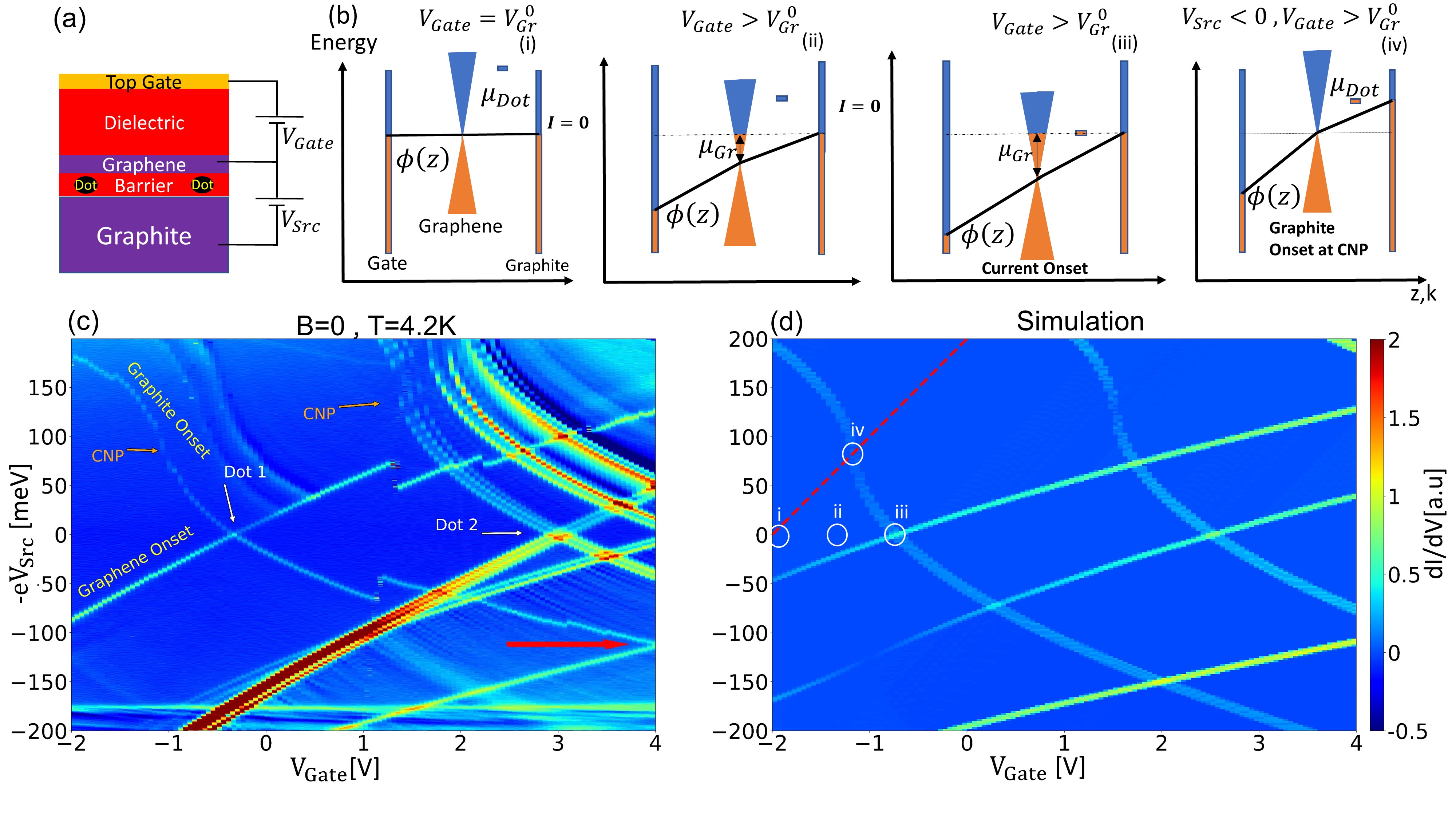
Capacitive model for defect-assisted tunneling
We take as a starting condition the neutrality point where graphene density is , = 0. At this condition we define (diagram (i)), where is the voltage required to offset any background density in the graphene. At neutrality, everywhere, and the dot energy is (we note that could vary depending on the type of defect Greenaway2018 ). The gate voltage affects the potential map by setting , being the thickness of the gate dielectric, and the absolute value of the electron charge. Applying positive gate voltage negatively charges the graphene layer. Throughout the measurement, graphene electrochemical potential is kept at ground: , and hence the accumulation of negative charge results in and a downward shift in .
Changing the graphene chemical potential modifies the dot energy, as is seen in diagrams (ii,iii). Here, an electric field penetrates to the gap between graphene and the source electrode at position . The dot, residing at position will change it chemical potential to . Current will flow through the dot only if or . Conduction onset at zero-bias will take place when the dot is resonant with both graphite source and graphene drain (diagram (iii)). In diagram (iv) we plot the condition of current onset at finite where . Here is applied concomitantly with to keep graphene density constant.
The source onset condition, where the dot potential is resonant with the source, is sensitive to changes in graphene chemical potential . This is seen by writing the dot potential as (Supplementary Note 1)
| (1) |
Using the source-onset condition, we find that traces up to a constant along the source onset line:
| (2) |
As we show in Supplementary Equation 11, this condition can be used to extract compressibility from the slope of the source onset line. As expected for single-layer graphene, the source-onset line traces a square-root dependence.
In Fig. 1(c) we identify the transport signatures of two distinct dots (Dot 1 and Dot 2), which likely reside in different regions and conduct in parallel (upon a 2nd cooldown, Dot 1 has shifted in gate voltage with respect to Dot 2). From Supplementary Equation 11, the maximal slope (absolute value), marked in the figure, is found where the graphene layer near each dot reaches the charge-neutrality point (CNP). Dot 1 has lower , and is accessible at lower density. Its charging energy, estimated from the crossing marked by a red arrow in the figure, is meV. We note that this is a higher value than found in similar studies Papadopoulos2019 ; Hakonen . Dot 2 appears at a higher density. It exhibits an energy splitting even at T (The origin of which is not presently understood).
Transport through the barrier dots is simulated by calculating a capacitive model of double-gated graphene sanchez with a fermi velocity of resulting in the differential conductance map shown in Fig. 1(d). In this model, capacitive charging is induced by the source and gate voltages following:
| (3) |
Where are the charge densities accumulated on the gate and source electrodes respectively, are the corresponding capacitances. The total charge is fixed to an initial .
| (4) |
and is related to by an integral on the DOS, :
| (5) |
Together, Equations 3 to 5 yield an integral equation for :
| (6) |
By numerically solving Equation 6 while using the known DOS of graphene , we find . Extracting using Equation 1, we obtain a differential conductance map for the contribution of each dot. From the simulation we extract meV for Dot 1 and meV for Dot 2. For both dots nm. Although we have no information about the chemical identity of the defects, the capacitive model places both of them at the center of the 5 layers.
Landau Level Spectroscopy
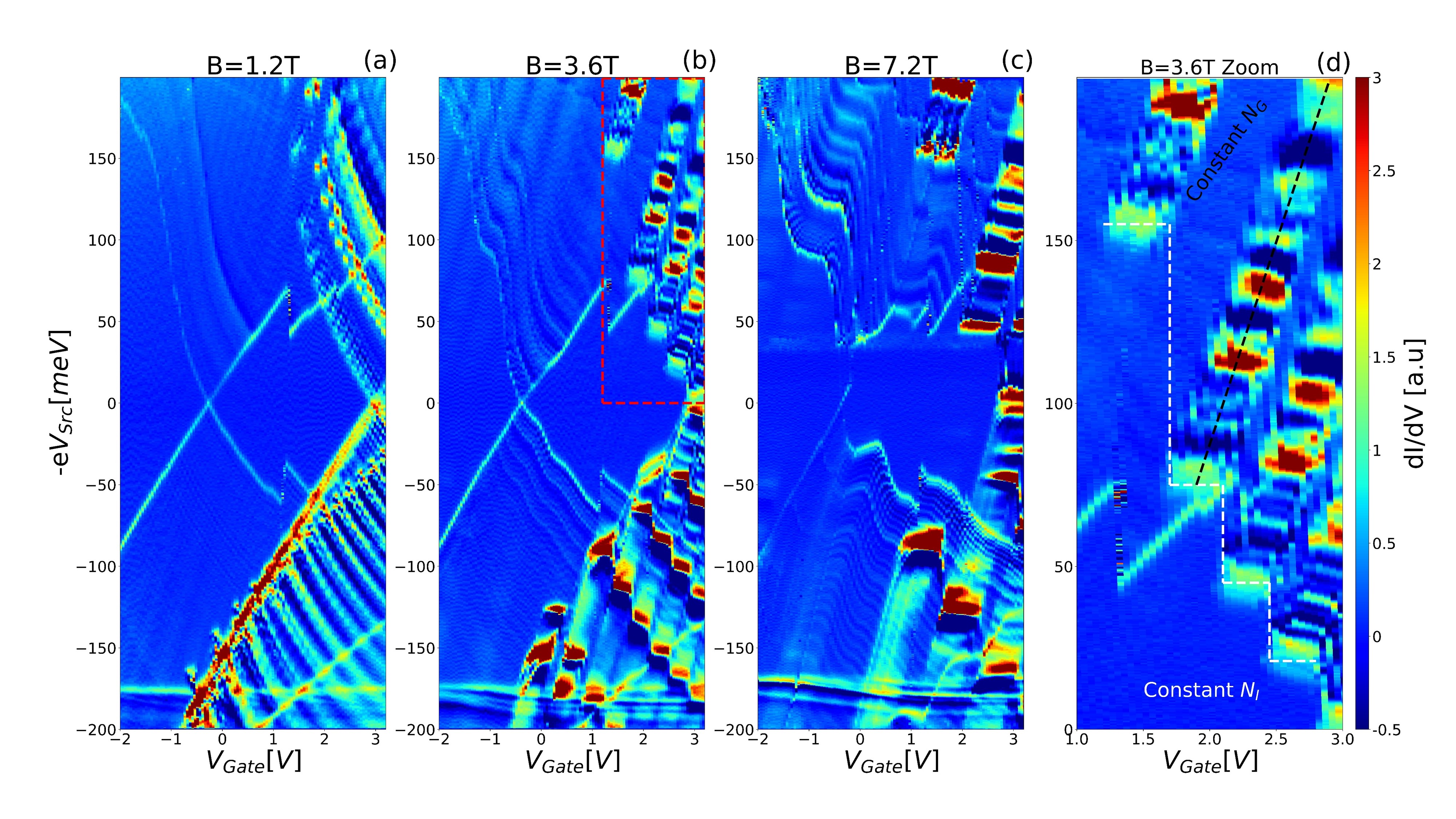
We now turn to the effect of perpendicular magnetic field on the transport through the quantum dot. In Fig. 2(b-d), we plot maps while applying magnetic fields of T, T, and T, respectively. The horizontal axis shows - a linear combination chosen such that graphene equal density lines are vertical. The same data, presented vs. , appear in Supplementary Figure 1. At the quantum Hall regime the onset of the dot transport attains a step-like structure in the (,) plane, characterized by flat conductance features whose width along the axis increases due to increasing Landau level degeneracy. To further elucidate the structure of these features, we focus on Dot 2, where steps are sharpest.
The origin of the step structure is in the Landau level DOS, as seen in Fig. 2(a) which depicts the energy diagram at a finite magnetic field. The DOS in the quantum Hall regime consists of discrete energy levels broadened due to disorder. In this regime, the onset of electron injection into graphene takes place when and at the same time the dot is resonant with an unpopulated Landau level:. A similar condition holds for electron ejection at the opposite bias. Panel (i) depicts such a resonant condition with electrons injected into Landau level . At the same time, the graphene Fermi energy resides within the Landau level. Since the measured spectrum depends both on the graphene ground state, and on the injection state, which are generally not the same, we designate each spectral feature by the respective pair of ground state and injection indices . () for injection (ejection) of electrons.
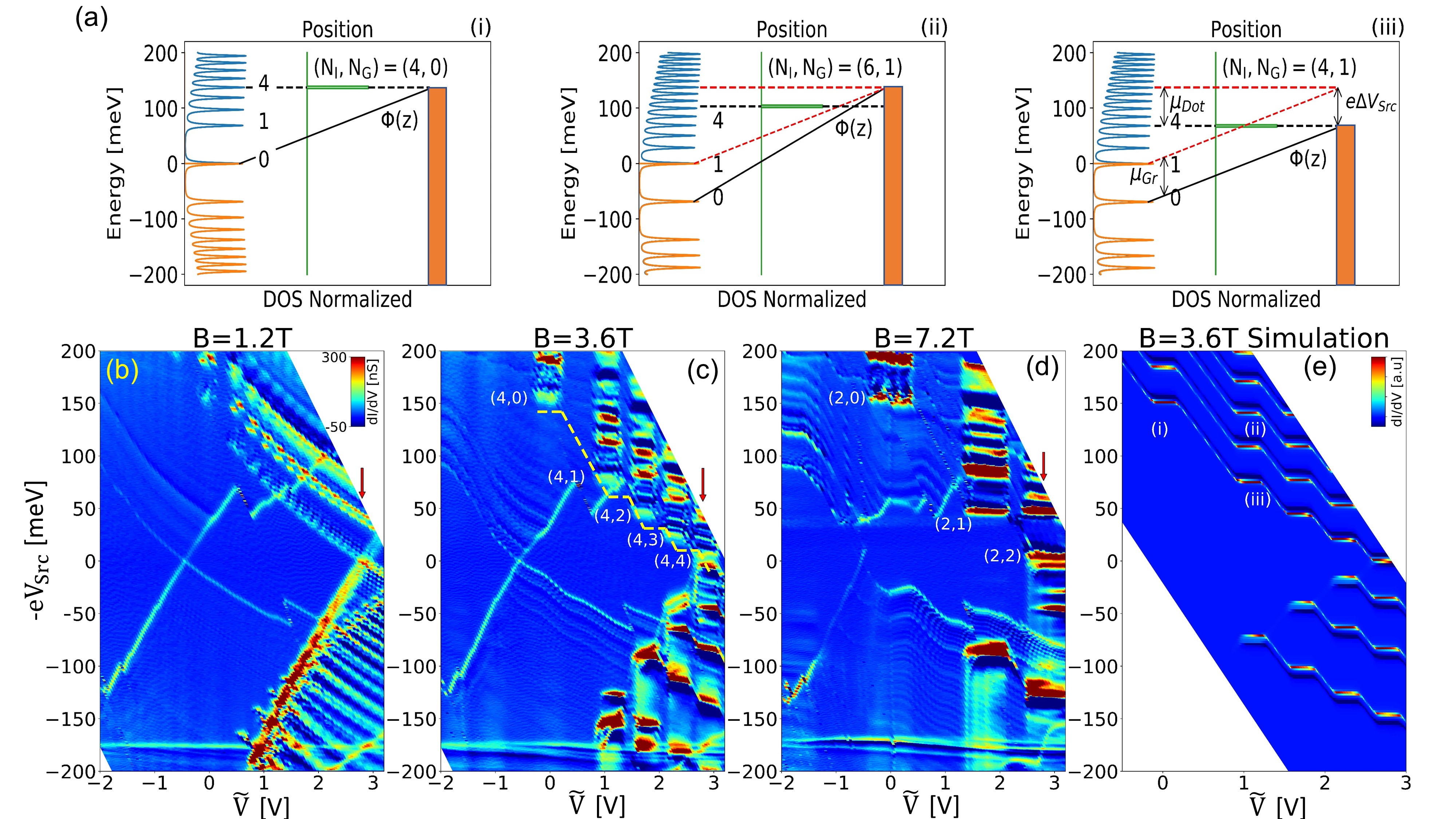
The feature of Dot 2 is found at (, meV) at all magnetic fields. The dashed line in Fig. 2(c) is the source-onset line in this field. Along this line the dot injects carriers to the same excited state , while the graphene electron density increases such that changes from to . This trajectory can be traced until , where the dot is resonant with the source and the drain, and electrons are injected into the ground state. At we have , identifying for this entire trajectory.
The (4,0) feature thus corresponds to the compressible regime, where resides within the Landau level, the DOS is very large, and graphene perfectly screens the electric field applied by the gate. Once this level is filled, graphene enters the incompressible regime. Its carrier density can not change - allowing almost perfect field penetration. As a result, shifts sharply downwards. The next compressible regime, corresponding to the ground state , appears at meV.
Between (4,0) and (4,1), the graphene ground state changes while the dot is kept resonant with the same injection level. Using Equation 1 we show in the Supplementary Notes 2,3 that along such a trajectory , where is the change in graphene chemical potential, and is the change in required to keep the same Landau level resonant. Using this relation, we find that the difference between the plateaus is meV, in agreement with the parameters used for the fit in Fig. 1(d). More generally, we can simulate the entire spectrum using the same model developed above (Equation 6), while assuming a density of states consisting of Gaussian broadened Landau levels. From the simulation we extract the source onset line corresponding to the trace. Plotted as a yellow dashed line in Fig. 2(c), this trace agrees very well with experimental data.
Degeneracy Lifting
The correspondence between and (Equation 2) shows that the source-onset line is sensitive to changes in and can hence be used as a compressibility probe (Supplementary Equation 11). In this sense, the barrier-defect functions as a very local single-electron transistor (SET) RevModPhys.64.849 ; Yoo1997 ; Wei1997 ; Ilani2004 . In what follows, we show that the dot also serves as a spectral probe, sensitive to excited state DOS. The dot is used as a spectrometer by keeping constant and scanning the injection energy, as explained schematically in panels (ii,iii) of Fig. 2(a). Here, is kept constant by balancing and , the dot energy follows . Thus, keeping the ground state fixed, the dot maps the spectra of different injection levels .
Barrier-dot-assisted spectroscopy is demonstrated in Fig. 3(a), where density is kept fixed at near dot 2 (marked by arrows in Fig. 2(b-d)). is scanned from to mV, corresponding to dot energies to meV (axis on the right of panel (b)). The spectrum is dominated by Landau levels whose energies follow the well known dependence, with kinks appearing as the graphene ground state shifts between compressible and incompressbile regimes. The simulation (panel (b)), based on the same model used above, reproduces this spectral map with excellent fidelity. The sharply peaked dot DOS causes the spectra measured this way to be extremely stable, since the DC contribution from levels below the dot energy is strongly suppressed. Compared to spectra measured using STMLuican2011 ; Stroscio2012 , it is seen here that the dot-assisted tunneling produces clear spectra at high bias, with well-resolved Landau levels at energies well over 150 meV. As we show below, the use of this probe on high quality encapsulated graphene samples reveals energy splitting related to the SU(4) degeneracy lifting in excited states.
In Fig. 3(a), two regions are marked, where the observed spectrum deviates from the calculation appearing in (b). In these regions, which correspond to injection of holes to the and levels, the spectral features are split due to lifting of the fourfold spin-valley degeneracy. The split spectral features of the state are extracted and plotted separately in panel (e). The spectrum consists of two peaks, which exhibit a separation of 6 meV visible at fields as low as T. This split remains fixed all the way to 9 T - suggesting a spin-independent origin. Since in the valley and sub-lattice degrees of freedom are coupled, this split could be due to a local breaking of sub-lattice symmetry - e.g. due to substrate effects, which should be independent of magnetic field.
At 6 T, a third spectral feature becomes visible. This feature, marked in red in panel (e), opens a gap which broadens rapidly (panel (f)). The gap, which evolves linearly with magnetic field, reaches a value of 17 meV at 9 T. It exhibits a very high slope: Extracting the factor using (where is the Bohr magneton), the observed split corresponds to for T, and for T (Fig. 3(f)). We can compare these values to STM measurements. For single-layer graphene on SiC Song2010 , the gap stands at 20 meV at 13 T. Another study, on tri-layer graphene, finds . He2018 Here we find that in our device the gap is both larger, and develops faster in magnetic field. Another large splitting appears at the feature. Extracting the split peak energies (Fig. 3(c)), we find an energy gap following a linear dependence with (Fig. 3(d)).
The origin of such large Zeeman splits is puzzling. In atomic defects , Dvir_PRL_2019 so the split is hence likely to originate in the graphene layer. Quantum Hall states are known to exhibit strong enhancements of the factors, associated with exchange coupling Abanin_2006 ; Sondhi_1993 . may vary with sample quality, increasing in cleaner samples where a larger number of carriers may be polarized Young2012 . The exchange energy split, predicted in Ref. Abanin_2006 is meV at 10 T - not far from the values we measure. Here, both the and states exhibit a split feature which extrapolates to zero at T, where . We thus speculate that the observed splitting is related to an interplay between the state of the injected carriers, and the onset of a spontaneous polarization at the state. In this scenario, the excited holes injected at the state undergo a strong exchange interaction with polarized spins in the ground state. This is plausible, since carriers at different Landau levels occupy the same spatial coordinates. Alternatively, the barrier dot which is 1 nm away from the graphene layer may itself experience strong exchange coupling to the graphene layer. Distinguishing between these two models requires calculations which are beyond the scope of the present work.
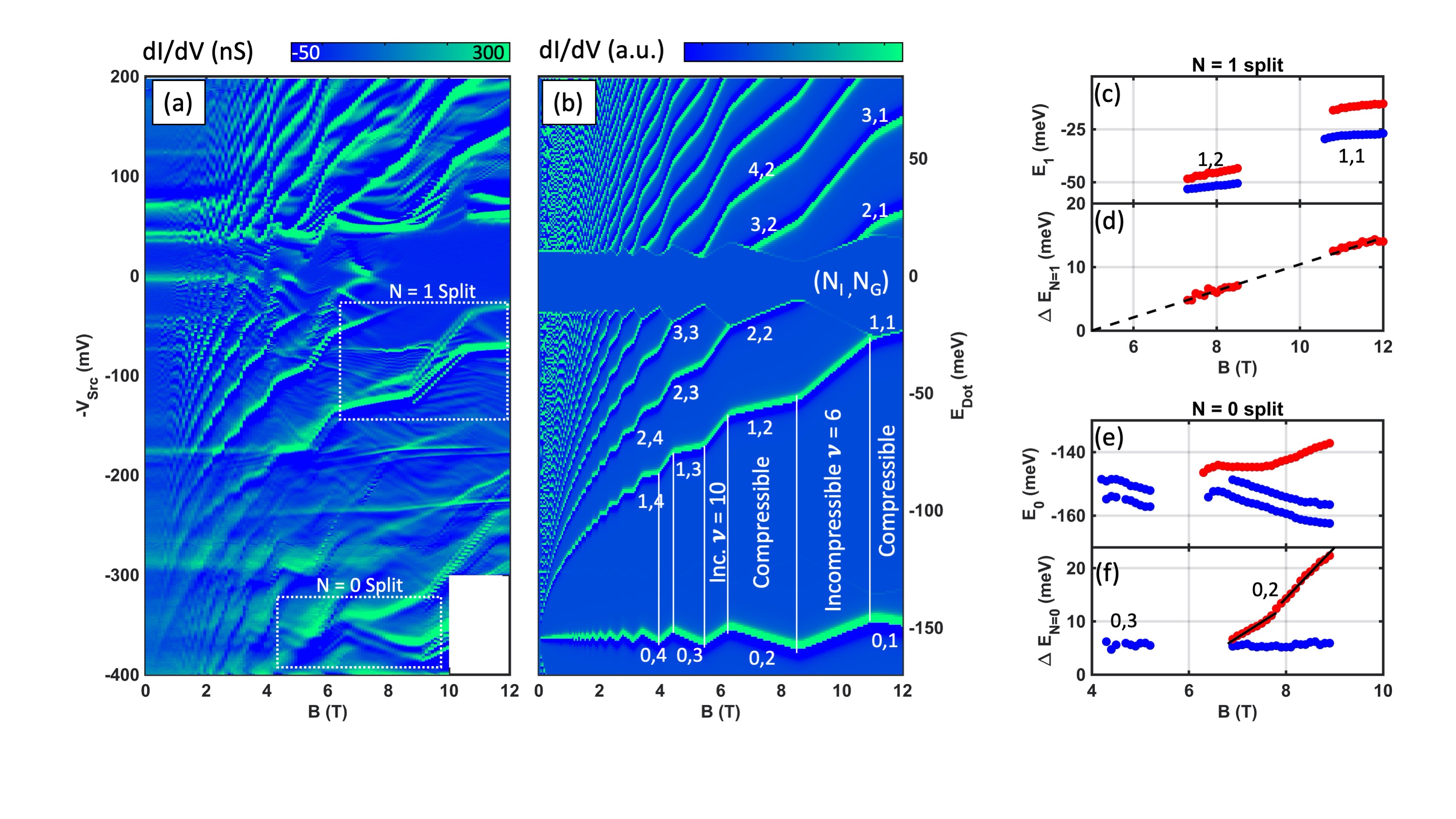
Turning our attention to energy splitting where the level is tuned to the ground state, we notice that the feature marked by (,) in Fig. 2(d) already shows incipient signatures of degeneracy lifting at T. Further increase of the magnetic field resolves the structure of the ( feature. The data, presented in Fig. 4, were taken at the high magnetic field facility in Grenoble at temperature K. In panel (a) we plot the spectra measured at T. We find spectral features corresponding to and . We focus on the manifold, where the continuous feature found at lower fields has separated into an intricate pattern consisting of 16 distinct features. The origin of this structure is in the four-fold degeneracy lifting of both ground state and injection state : As we’ve seen in Fig. 3, tuning maps the excited state spectrum at the injection level - in this case . At this high magnetic field, all four levels are distinguishable - as seen also at the fixed-density line-cuts, presented in panel (c). Along the horizontal () axis, the breakup into four features is a consequence of degeneracy lifting in the ground state. The spectrum clearly exhibits narrow incompressible regions, corresponding to fill factors .
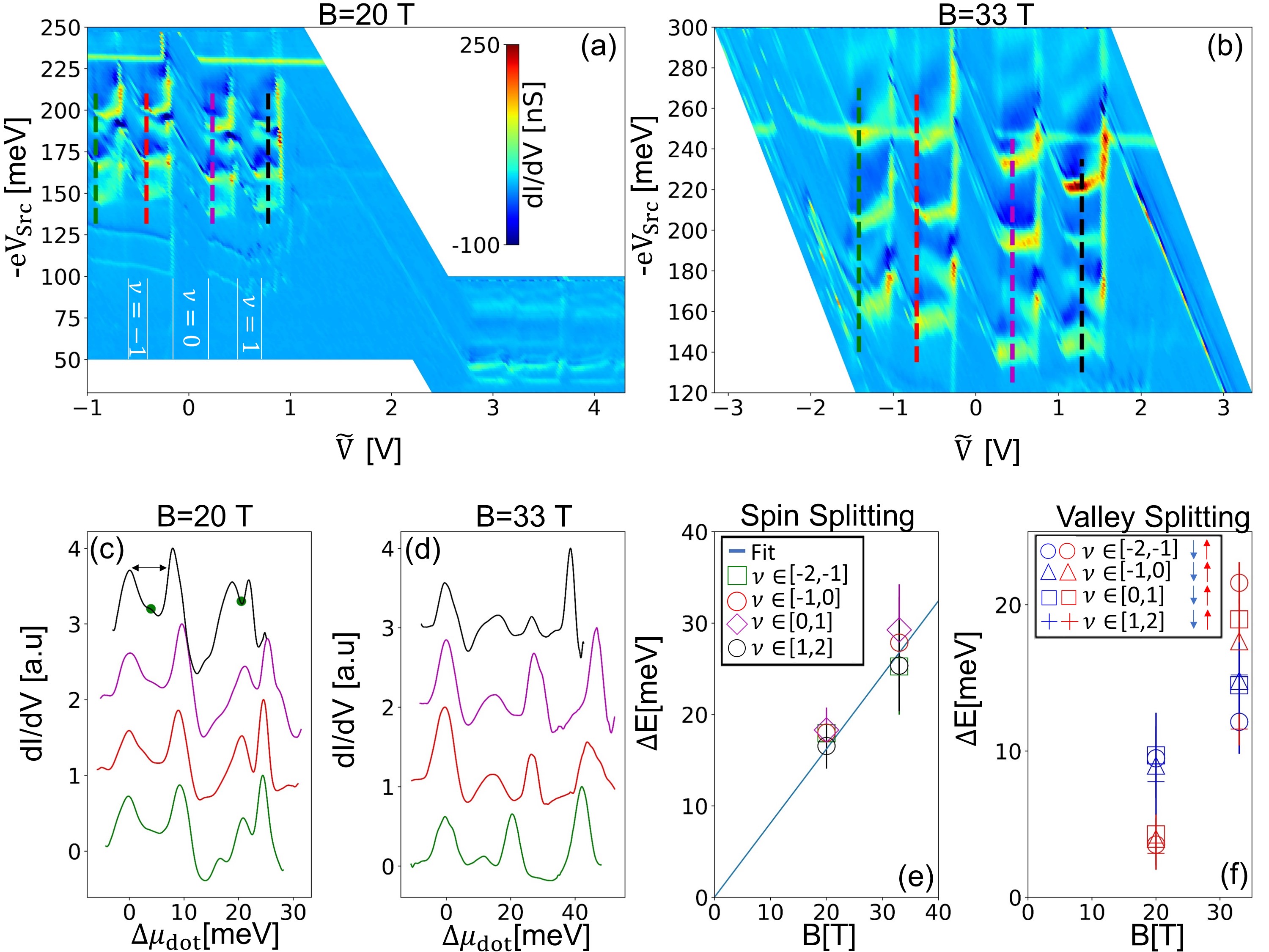
To understand which degeneracy drives the dominant splitting, we measure the energy difference between the mean of the two low energy peaks and the mean of the two high energy peaks of the spectra in Fig. 4(c,d). The differences between these means (green dots in panel (c)), , are plotted in Fig. 4(e). For each of the available magnetic field data sets (B = 20, 33 T), we have four data points - corresponding to the different ground states and . As seen in panel (e), at each magnetic field all four points are bunched closely together. A single fit for can be used for all fill factors. The fit follows a straight line which extrapolates to zero, implying that Zeeman splitting is the leading degeneracy lifting term, in agreement with early transport measurements PhysRevLett.96.136806 ; PhysRevLett.99.106802 . The slope yields . Splitting the level should be compared to transport results with a ground state fill factor . We find a greater factor than those found before, where excitations at yielded . Young2012 A number of causes could explain this difference. First, in Ref Young2012 , the gap is measured via temperature dependence of a macroscopic sample, with being the ground state. Here, we measure the spectrum of an excited state, with being the ground state. Second, our measurement is local, and is hence less prone to averaging effects of disorder.
Having identified the leading split with the Zeeman term, we associate the two lower energy states with spin up, and the two higher energy states with spin down. In Fig. 4(f) we plot the energy difference within each same-spin pair. It is evident that in all fill factors, the gap between spin-down states (blue markers) increases, but by a lesser amount with respect to the gap between spin up states (red markers). This result indicates that the valley splitting depends on the spin state, suggesting a coupling between the valley and spin degrees of freedom. Coupling between spin and valley degeneracy lifting has been discussed in graphene quantum dots localized by STM tips Freitag_2016 ; Li_STM_2019 ; Luican_2014_STM , where strong confinement lifts orbital degeneracy. Our system lacks a strong confining potential. Even if the dot is charged, the charging field should be screened at the compressible limit.
Here we suggest that valley splitting could be indicative of the nature of the ground state. In the Anti-ferromagnetic (AF) or canted anti-ferromagnetic (CAF) ground states, for example, spin is coupled to the sub-lattice degree of freedom, which translates to the valley degree of freedom at . In Fig. 4, electrons are injected into the level while . We speculate that for the single-particle state of the injected spin-polarized electron, the valley degree of freedom will dictate its relative overlap with the spins of the many-body ground state. While this calls for further calculation, it is likely the ferromagnetic (F) state can be ruled out when such splitting is observed.
Discussion
Based on the compiled values of degeneracy lifted energy splitting (Table 1) we can conclude that exchange interactions appear to play a major role in the spin-split state in high quality samples. The spin-split features measured in Fig. 3 develop within a very small window in magnetic field - suggesting some pre-condition for their onset. In addition, we find that the ground state plays an important role in determining the excited state spectrum. The feature develops differently when the ground state is () and when (). This could be possible if, indeed, the splitting is governed by exchange interactions - since the injected / ejected carrier will experience the strongest interactions with carriers in the ground state. Finally, we find that a non-trivial interplay exists between spin and valley splitting.
| 2,3 | 0 | 100-160 | 4-9 | Fig. 3 |
| 1,2 | 1 | 36 | 6-12 | Fig. 3 |
| 0 | 1 | 14 | 20-33 | Fig. 4 |
At high magnetic fields, we also notice that the barrier dot becomes sensitive to the transition between compressible and incompressible regimes. As seen in Fig. 4(a,b), upon filling each Landau level the dot energy shifts vertically up before turning down again. We suggest that the sharp evolution of the density-dependent dot spectrum is a consequence of dot sensitivity to local disorder potential, which forms electrically floating regions in the graphene layer. Since the observed feature appears close to the full Landau level limit, the floating compressible island should be hole-like, and is coupled to a local potential maximum. Interestingly, such maximum could be induced by the negative charge of the dot itself Luican_2014_STM ; Wong_Defects_2015 . Confirming this, however, will require further study with additional samples.
Our results demonstrate the efficacy of barrier-dot-assisted spectroscopy as a probe for graphene in strongly-interacting quantum Hall states. The wide values of energy splitting away from the ground state suggest that strong exchange interaction has to be considered between excited carriers and polarized ground states. The observation of such features indicates that the barrier dot, as a probe, retains fragile many-body states. This could be the consequence of minimal screening, planar geometry, or both. As barrier dots may also serve as local sensors for the chemical potential, they thus merge the capabilities of local SETs RevModPhys.64.849 ; Yoo1997 ; Wei1997 ; Ilani2004 with probes which retain planar geometry Dial_2007 . Their size, positioning and non-invasiveness thus make barrier dots potentially useful probes for other interacting systems.
Methods
Device Fabrication
The vdW tunnel junction was fabricated using the vdW transfer technique. The graphite flake was exfoliated on a SiO2 substrate. The hBN barrier and graphene flakes were transferred on top of the graphite flake, respectively. On top of the graphene flake, another bulk hBN flake was transferred, with the purpose of acting as a gate dielectric. Ti/Au contacts were fabricated using standard electron beam lithography techniques. Contact evaporation was executed at high vacuum and at C.
Acknowledgements
The authors are thankful for discussions with S. Ilani, D.Orgad, A. Yacoby, P. Jarillo-Herrero, E. Rossi and E. Andrei. M. Aprili, C. H. L. Quay and M. Kuzmenovic assisted with high magnetic field measurements. Device fabrication and characterization were carried out at the Harvey M. Krueger Family Center for Nanoscience and Nanotechnology. Part of this work was performed at the LNCMI, a member of the European Magnetic Field Laboratory. Work was supported by ERC-2014-STG Grant No. 637298 and ISF Quantum Initiative grant No. 994/19. A.Z. and T. D. Are supported by an Azrieli Fellowship. K.W. and T.T. acknowledge support from the Elemental Strategy Initiative conducted by the MEXT, Japan and and the CREST (JPMJCR15F3), JST.
Author Contributions
I. K., T. D. and A. I. fabricated the device. Measurements were carried out by I. K. and A. Z.. Data were analysed by I. K.. High Field measurements were done by D. L.. K. W. and T. T. provided the hBN. Manuscript was drafted by I. K. and H. S.. H. S. supervised the project.
I Supplementary Information
Supplementary Note 1. Dot Potential
We calculate the dot potential assuming a grounded graphene layer, . As seen in Figure 1(b) in the main text, since , we have . The electric field between the graphene and the source is:
| (S1) |
The electric potential at the dot location obeys:
| (S2) |
The dot energy is shifted by from the potential at :
| (S3) |
Supplementary Note 2. Extracting DOS from Slope
From the resonant features in Fig. 1(c), we can extract the density of states, and quantum capacitance, using two equations. The first is the integral equation (Equation (6) in the main text) for the graphene chemical potential :
| (S4) |
which relates , and . The solution to this equation defines the charge density for any gate and bias voltage.
Along source onset line, where the dot is resonant with the source electrode, we have . Plugging it into the source-dot resonance condition (Equation S3) we have:
| (S5) |
This yields the equation
| (S6) |
Where the last equation means that to stay on resonance, will trace the graphene chemical potential up to a constant. We use two equations: The integral equation, Equation S4, and Equation S6. These two depend on , and . We are interested in an expression for a slope in the (,) plane: . To reach this, we plug Equation S6 into Equation S4:
| (S7) |
From which we isolate
| (S8) |
Yielding
| (S9) |
From Equation S6:
| (S10) |
Thus
| (S11) |
Supplementary Note 3. Resonant Trajectory
In the specific case where the quantum dot traces the spectrum of a Landau level, as in Figure 2, we can reach a special case of Equation (2) (Equation S6), showing that upon a transition between two Landau levels. We calculate the shift in between the two compressible plateaus corresponding to the difference between the and Landau levels. This is elucidated in the three schematic energy diagrams presented in Figure 2(a) in the main text, where the trajectory from (4,0) to (4,1) is broken into two stages. First, is a transition from (i) to (ii) along a fixed line, graphene shifts from ground state , with chemical potential to ground state with chemical potential . From Equation (1) (Equation S3) we find the dot energy shift is:
| (S12) |
Here is the difference in the graphene chemical potential upon increase of a single Landau level. In the second leg of the trajectory, from (ii) to (iii), the dot is brought back to resonance with the same through a shift in while keeping (and ) fixed. Here Equation (1) yields
| (S13) |
The total shift in from (i) to (iii) is
| (S14) |
Demanding that the dot remains resonant with the same Landau level requires:
we have
which yields
| (S15) |
This relation is general for trajectories where the dot is kept in resonance with a specific spectral feature. In our case it means that tuning the system from from (i) to (iii), while changing the graphene ground state from to results in . This is also demonstrated in panel (iii) of Figure 2 in the main text, where we find that corresponding to state (i), plotted in red, is parallel to the new corresponding to state (iii), plotted in black.
Supplementary Note 4. Raw Data
In the main text, the horizontal axis used in Fig. 2 and Fig. 4 shows , defined such that the graphene equal density lines are vertical - leading to easier identification of the energy difference between Landau levels. In Supplementary Figure 1 we show the raw data, where the horizontal axis is . Panels (a-c) show the same measurements presented in Fig. 2 while panel (d) shows the region marked by a red square in (b), zoomed in. This representation of the data enables appreciation of the sharpness of the transition between adjacent ground states.
From Supplementary Figure 1(d) it is evident that the transition, along a constant injection trajectory, between adjacent ground states is vertical. This embodies the fact that once a Landau level is full, further gating the graphene with little additional charge shifts its spectrum by the energy difference between levels. Along a constant injection trajectory, compensates for this shift resulting in the vertical staircase structure.
Supplementary Note 5. Device Details
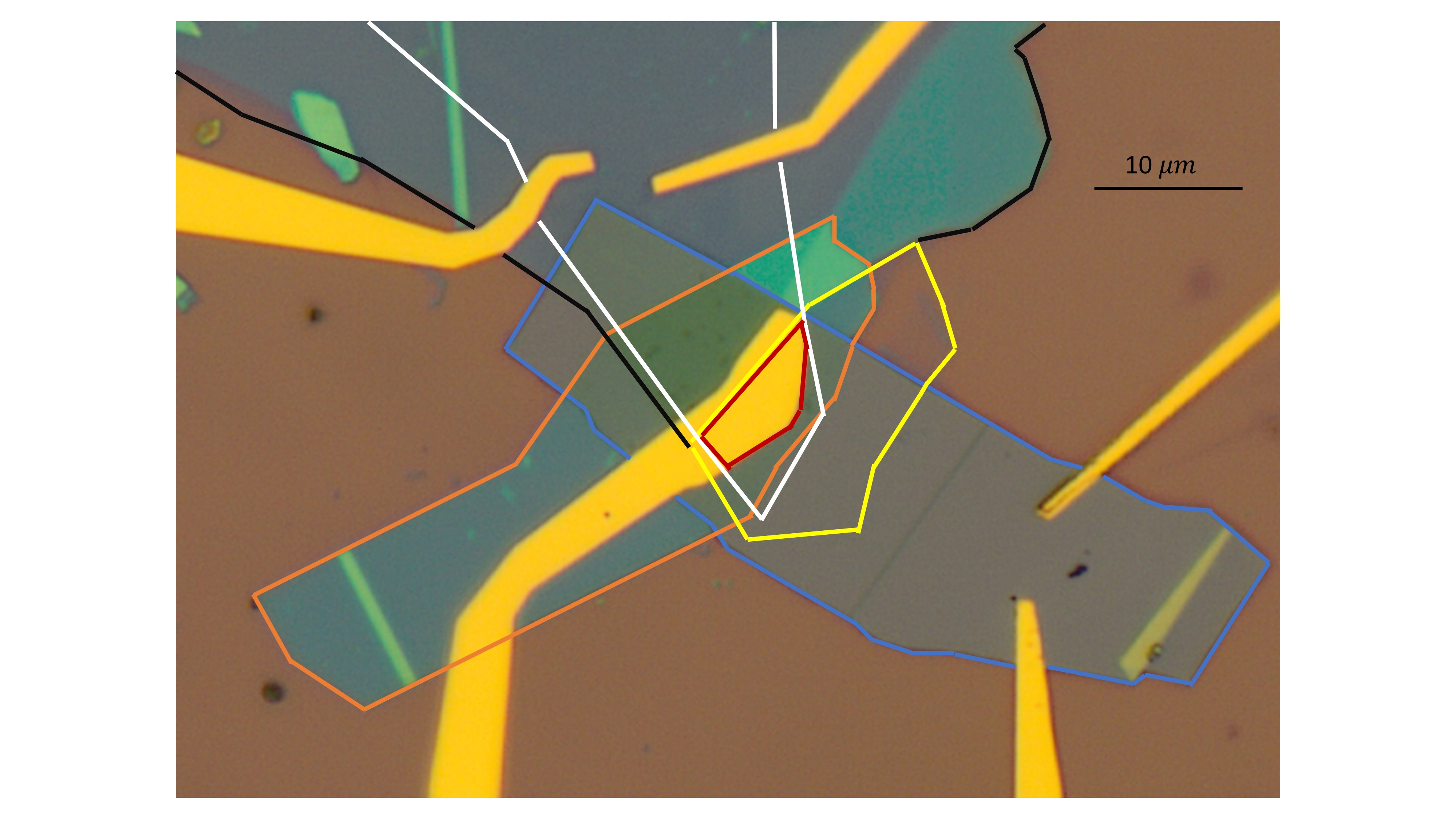
The data in this work originates from a single device consisting of two dots within a region of approximately 45 pictured in Supplementary Figure 2.
In Supplementary Figure 2 one can see an overlap between graphene (white), barrier hBN (yellow) and graphite (blue) away from the gated region (red). This leads to the possibilty of un-gated dots and might explain the constant feature near -180 meV in Supplementary Figure 1 as an additional un-gated dot. The area of the un-gated region is approximately 30 . All together, our junction has 3 dots over the region of 75 which leads to the estimate of one dot per 25 . We note that this represents a smaller dot density than reported in Ref. Greenaway2018 . Based on these dimensions, and on dimensions of devices measured by others Greenaway2018 ; Chandni2015 ; Chandni2016 , to obtain transport-active dots, one requires a gated junction area should be 20-30 and barrier hBN thickness 3-6 layers.
References
References
- (1) Giaever, I. Energy Gap in Superconductors Measured by Electron Tunneling. Phys. Rev. Lett. 5, 147–148 (1960).
- (2) Wolf, E. L. Principles of electron tunneling spectroscopy (Oxford University Press, 2012), 2nd edn.
- (3) Binnig, G., Rohrer, H., Gerber, C. & Weibel, E. Surface studies by scanning tunneling microscopy. Phys. Rev. Lett. 49, 57–61 (1982).
- (4) Jung, S. et al. Evolution of microscopic localization in graphene in a magnetic field from scattering resonances to quantum dots. Nature Physics 5, 1–7 (2011).
- (5) Wang, Y. et al. Mapping Dirac quasiparticles near a single Coulomb impurity on graphene. Nature Physics 8, 653–657 (2012).
- (6) Zhao, Y. et al. Creating and probing electron whispering-gallery modes in graphene. Science 348, 672–675 (2015).
- (7) Brar, V. W. et al. Gate-controlled ionization and screening of cobalt adatoms on a graphene surface. Nature Physics 7, 43–47 (2011).
- (8) Zhang, Y., Tan, Y.-W., Stormer, H. L. & Kim, P. Experimental observation of the quantum Hall effect and Berry’s phase in graphene. Nature 438, 201–204 (2005).
- (9) Luican, A., Li, G. & Andrei, E. Y. Quantized Landau level spectrum and its density dependence in graphene. Physical Review B 83, 041405 (2011).
- (10) Greenaway, M. T. et al. Tunnel spectroscopy of localised electronic states in hexagonal boron nitride. Communications Physics 1, 94 (2018).
- (11) Dvir, T., Aprili, M., Quay, C. H. L. & Steinberg, H. Zeeman Tunability of Andreev Bound States in van der Waals Tunnel Barriers. Physical Review Letters 123, 217003 (2019).
- (12) Mishchenko, A. et al. Twist-controlled resonant tunnelling in graphene/boron nitride/graphene heterostructures. Nature Nanotechnology 9, 808–813 (2014).
- (13) Venkatachalam, V., Hart, S., Pfeiffer, L., West, K. & Yacoby, A. Local thermometry of neutral modes on the quantum Hall edge. Nature Physics 8, 676–681 (2012).
- (14) Maradan, D. et al. GaAs Quantum Dot Thermometry Using Direct Transport and Charge Sensing. J. Low Temp. Phys. 175, 784–798 (2014).
- (15) Deng, M. T. et al. Majorana bound state in a coupled quantum-dot hybrid-nanowire system. Science 354, 1557–1562 (2016).
- (16) Jünger, C. et al. Spectroscopy of the superconducting proximity effect in nanowires using integrated quantum dots. Communications Physics 2, 76 (2019).
- (17) Alicea, J. & Fisher, M. P. A. Graphene integer quantum Hall effect in the ferromagnetic and paramagnetic regimes. Physical Review B 74, 075422 (2006).
- (18) Goerbig, M. O., Moessner, R. & Doucot, B. Electron interactions in graphene in a strong magnetic field. Physical Review B 74, 161407 (2006).
- (19) Yang, K., Das Sarma, S. & MacDonald, A. H. Collective modes and skyrmion excitations in graphene SU(4) quantum hall ferromagnets. Phys. Rev. B 74, 075423 (2006).
- (20) Nomura, K. & MacDonald, A. H. Quantum hall ferromagnetism in graphene. Phys. Rev. Lett. 96, 256602 (2006).
- (21) Kharitonov, M. Phase diagram for the =0 quantum Hall state in monolayer graphene. Physical Review B 85, 155439 (2012).
- (22) Fuchs, J.-N. & Lederer, P. Spontaneous parity breaking of graphene in the quantum hall regime. Phys. Rev. Lett. 98, 016803 (2007).
- (23) Young, A. F. et al. Spin and valley quantum Hall ferromagnetism in graphene. Nature Physics 8, 550–556 (2012).
- (24) Jiang, Z., Zhang, Y., Stormer, H. L. & Kim, P. Quantum hall states near the charge-neutral dirac point in graphene. Phys. Rev. Lett. 99, 106802 (2007).
- (25) Zhang, Y. et al. Landau-level splitting in graphene in high magnetic fields. Phys. Rev. Lett. 96, 136806 (2006).
- (26) Song, Y. J. et al. High-resolution tunnelling spectroscopy of a graphene quartet. Nature 467, 185–189 (2010).
- (27) Li, S.-Y., Zhang, Y., Yin, L.-J. & He, L. Scanning tunneling microscope study of quantum Hall isospin ferromagnetic states in the zero Landau level in a graphene monolayer. Physical Review B 100, 085437 (2019).
- (28) Chakraborty, C., Kinnischtzke, L., Goodfellow, K. M., Beams, R. & Vamivakas, A. N. Voltage-controlled quantum light from an atomically thin semiconductor. Nature Nanotechnology 10, 507–511 (2015).
- (29) He, Y.-M. et al. Single quantum emitters in monolayer semiconductors. Nature Nanotechnology 10, 497 (2015).
- (30) Tran, T. T. et al. Robust multicolor single photon emission from point defects in hexagonal boron nitride. ACS Nano 10, 7331–7338 (2016).
- (31) Dvir, T. et al. Spectroscopy of bulk and few-layer superconducting NbSe2 with van der Waals tunnel junctions. Nature Communications 9, 598 (2018).
- (32) Dvir, T., Aprili, M., Quay, C. H. L. & Steinberg, H. Tunneling into the Vortex State of NbSe2 with van der Waals Junctions. Nano Letters 18, 7845–7850 (2018).
- (33) Chandni, U., Watanabe, K., Taniguchi, T. & Eisenstein, J. P. Evidence for Defect-Mediated Tunneling in Hexagonal Boron Nitride-Based Junctions. Nano Letters 15, 7329–7333 (2015).
- (34) Papadopoulos, N. et al. Tunneling spectroscopy of localized states of WS2 barriers in vertical van der Waals heterostructures. Physical Review B 101, 165303 (2020).
- (35) Khanin, Y. N. et al. Tunneling in graphene/h-BN/graphene heterostructures through zero-dimensional levels of defects in h-BN and their use as probes to measure the density of states of graphene. JETP Letters 109, 482–489 (2019).
- (36) Hong, J. et al. Exploring atomic defects in molybdenum disulphide monolayers. Nature Communications 6, 197 (2015).
- (37) Liu, Y. et al. Defects in h-BN tunnel barrier for local electrostatic probing of two dimensional materials. APL Materials 6, 091102 (2018).
- (38) Sanchez-Yamagishi, J. D. et al. Quantum hall effect, screening, and layer-polarized insulating states in twisted bilayer graphene. Phys. Rev. Lett. 108, 076601 (2012).
- (39) Kastner, M. A. The single-electron transistor. Rev. Mod. Phys. 64, 849–858 (1992).
- (40) Yoo, M. J. Scanning Single-Electron Transistor Microscopy: Imaging Individual Charges. Science 276, 579–582 (1997).
- (41) Wei, Y. Y., Weis, J., von Klitzing, K. & Eberl, K. Single-electron transistor as an electrometer measuring chemical potential variations. Applied Physics Letters 71, 2514–2516 (1997).
- (42) Ilani, S. et al. The microscopic nature of localization in the quantum Hall effect. Nature 427, 328–332 (2004).
- (43) Chae, J. et al. Renormalization of the graphene dispersion velocity determined from scanning tunneling spectroscopy. Phys. Rev. Lett. 109, 116802 (2012).
- (44) Zhang, Y., Qiao, J.-B., Yin, L.-J. & He, L. High-resolution tunneling spectroscopy of ABA-stacked trilayer graphene. Physical Review B 98, 1–6 (2018).
- (45) Abanin, D. A., Lee, P. A. & Levitov, L. S. Spin-Filtered Edge States and Quantum Hall Effect in Graphene. Physical Review Letters 96, 176803 (2006).
- (46) Sondhi, S. L., Karlhede, A., Kivelson, S. A. & Rezayi, E. H. Skyrmions and the crossover from the integer to fractional quantum Hall effect at small Zeeman energies. Physical Review B 47, 16419–16426 (1993).
- (47) Freitag, N. M. et al. Electrostatically Confined Monolayer Graphene Quantum Dots with Orbital and Valley Splittings. Nano Letters 16, 5798–5805 (2016).
- (48) Luican-Mayer, A. et al. Screening Charged Impurities and Lifting the Orbital Degeneracy in Graphene by Populating Landau Levels. Physical Review Letters 112, 036804 (2014).
- (49) Wong, D. et al. Characterization and manipulation of individual defects in insulating hexagonal boron nitride using scanning tunnelling microscopy. Nature Nanotechnology 10, 949–953 (2015).
- (50) Dial, O. E., Ashoori, R. C., Pfeiffer, L. N. & West, K. W. High-resolution spectroscopy of two-dimensional electron systems. Nature 448, 176–179 (2007).
- (51) Chandni, U., Watanabe, K., Taniguchi, T. & Eisenstein, J. P. Signatures of Phonon and Defect-Assisted Tunneling in Planar Metal-Hexagonal Boron Nitride-Graphene Junctions. Nano Letters 16, 7982–7987 (2016).