Field-free switching of magnetic tunnel junctions driven by spin-orbit torques at sub-ns timescales
Abstract
We report time-resolved measurements of magnetization switching by spin-orbit torques in the absence of an external magnetic field in perpendicularly magnetized magnetic tunnel junctions (MTJ). Field-free switching is enabled by the dipolar field of an in-plane magnetized layer integrated above the MTJ stack, the orientation of which determines the switching polarity. Real-time single-shot measurements provide direct evidence of magnetization reversal and switching distributions. Close to the critical switching voltage we observe stochastic reversal events due to a finite incubation delay preceding the magnetization reversal. Upon increasing the pulse amplitude to twice the critical voltage the reversal becomes quasi-deterministic, leading to reliable bipolar switching at sub-ns timescales in zero external field. We further investigate the switching probability as a function of dc bias of the MTJ and external magnetic field, providing insight on the parameters that determine the critical switching voltage.
Current-induced spin-orbit torques (SOT) allow for manipulating the magnetization of diverse classes of magnetic materials and devices Manchon et al. (2019); Miron et al. (2011a); Liu et al. (2012); Cubukcu et al. (2014); Fukami et al. (2016a); Lee and Lee (2016); Luo et al. (2020). Recent studies on ferromagnetic nanodots and magnetic tunnel junctions (MTJ) have shown that SOT-induced switching can overcome spin transfer torque (STT) switching in terms of speed, reliability, and endurance Garello et al. (2014); Zhang et al. (2015); Aradhya et al. (2016); Baumgartner et al. (2017); Yoon et al. (2017); Decker et al. (2017); Cubukcu et al. (2018); Kato et al. (2018); Grimaldi et al. (2020). Fast and reliable deterministic switching of MTJs is especially important for the development of non-volatile magnetic random access memories Kent and Worledge (2015); Apalkov, Dieny, and Slaughter (2016); Prenat et al. (2016). However, when switching a perpendicular magnetization by SOT, a static in-plane magnetic field is required to break the torque symmetry, which otherwise does not discriminate between up and down magnetic states Miron et al. (2011a). As such field is detrimental for memory applications, various approaches have been proposed to achieve field-free SOT switching, including exchange coupling to an antiferromagnet Fukami et al. (2016b); Oh et al. (2016); van den Brink et al. (2016), RKKY Lau et al. (2016) and Dzyaloshinskii-Moriya Luo et al. (2019) coupling to a reference ferromagnet, tilted magnetic anisotropy You et al. (2015), geometrical asymmetry Yu et al. (2014); Safeer et al. (2016); Chen et al. (2018), and two-pulse schemes van den Brink et al. (2014); Wang et al. (2018); de Orio et al. (2019). An alternative approach, compatible with back-end-of-line integration of MTJs on CMOS wafers, is based on embedding a ferromagnet in the hard mask that is used to pattern the SOT current line Garello et al. (2019). In such devices, the rectangular shape of the magnetic hard mask (MHM) provides strong shape anisotropy along the current direction, thus generating an in-plane field on the free layer without imposing additional overheads on the processing and power requirements of the MTJs [Fig. 1(a)].
In this letter, we report on real-time measurements of field-free magnetization switching in three-terminal MTJs including a MHM. Whereas the switching dynamics has been extensively studied in two-terminal MTJs operated by STT Devolder et al. (2008); Tomita et al. (2008); Cui et al. (2010); Hahn et al. (2016); Devolder, Le Goff, and Nikitin (2016); Devolder et al. (2016), there are only few studies addressing the transient dynamics and real-time reversal speed of individual SOT-induced switching events in three-terminal MTJs Grimaldi et al. (2020); Inokuchi et al. (2019). In particular, the SOT-induced dynamics, reversal speed, and critical voltage in MTJs with perpendicular magnetization have not been investigated in the absence of an external magnetic field.
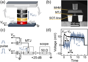
Our devices are top-pinned MTJs with 108% tunneling magnetoresistance (TMR) patterned into a circular pillar with a diameter of 80 nm. The pillars are grown on top of a 190 nm wide -W SOT-current line with resistivity of cm and resistance of . The MTJ is formed by free and reference layers made of CoFeB with a thicknesses of 0.9 and 1 nm, respectively, separated by an MgO tunnel barrier with resistance-area product of 20 m2, as shown in Fig. 1(a). The reference layer (yellow) is pinned to a synthetic antiferromagnet (black, SAF). The reference layer and the SAF generate an out-of-plane dipolar field mT that favors the anti-parallel (AP) over the parallel (P) state of the MTJ. The hard mask used to pattern the SOT line incorporates a 50 nm thick Co magnetGarello et al. (2019), which provides an in-plane field ( mT) parallel to the SOT line [Figs. 1(a) and (b)]. Due to its high aspect ratio of nm2, the magnetization direction of the Co hard mask remains constant after saturation. Moreover, the magnetization of the hard mask is not influenced by pulsing the current either through the SOT line or the MTJ pillar.
Electrical measurements are performed using a setup that combines real-time and after-pulse readout of the MTJ resistance, as depicted in Fig. 1(c) and reported in more detail in Ref. Grimaldi et al., 2020. After-pulse switching measurements consist of an initialization pulse that sets the free layer magnetization in the desired state, which is verified by a dc measurement of the MTJ resistance, and a switching pulse, also followed by a dc resistance measurement. In the time-resolved measurements, a driving voltage supplied by a pulse generator with 0.15 ns rise time is split in two pulses with a well-defined amplitude that are simultaneously fed to the input electrodes of the three-terminal MTJ device. The pulse applied to the bottom electrode () drives the SOT reversal. Together, the pulse applied to the top electrode and determine the potential difference across the MTJ pillar (). By adjusting the ratio between these pulse amplitudes, we control the instantaneous value of , which allows for studying phenomena emerging from the bias during SOT-driven reversal, such as voltage control of magnetic anisotropy (VCMA) as well as STT switching Grimaldi et al. (2020). In this work, we restrict ourselves to switching at zero, low, and strong bias ( = 0, -0.5 and -1.65 ). The pulse transmitted through the device is amplified and acquired on a 20 GHz sampling oscilloscope, which allows for monitoring the MTJ resistance in real-time in a time window defined by the width of the driving pulse. To facilitate the analysis of different switching events, a reference trace is subtracted to each voltage trace recorded during a switching pulse. The reference trace is obtained by maintaining the MTJ in its initial state, either P or AP, by application of an external magnetic field opposing . The resultant trace is then divided by the voltage difference between the P and AP states [Fig. 1(d)] in order to obtain the normalized switching signal .
Time-resolved studies of current-induced switching can be performed either by pump-probe measurements Baumgartner et al. (2017); Decker et al. (2017); Yoon et al. (2017), which yield the average magnetization dynamics, or single-shot measurements Devolder et al. (2008); Tomita et al. (2008); Cui et al. (2010); Hahn et al. (2016); Devolder, Le Goff, and Nikitin (2016); Devolder et al. (2016); Inokuchi et al. (2019); Grimaldi et al. (2020). Although average time-resolved measurements provide information on the reproducible dynamic behavior of the magnetization and afford a higher signal-to-noise ratio compared to single-shot measurements, stochastic dynamical processes can only be revealed in studies carried out on individual switching events. In this study we perform both types of measurements to highlight different aspects of the reversal dynamics. In order to provide a measurable tunneling magnetoresistance reading in single-shot measurements, we apply a small voltage bias on the MTJ to allow for current flow through the pillar. Depending on the sign of relative to , this bias can either assist or hinder the SOT switching. Two effects are induced by , namely the STT and VCMA. As the sign of the STT depends on the orientation of the reference layer and the VCMA does not, these two effects can be disentangled from each other Grimaldi et al. (2020). Here, we set the sign of such that STT always opposes SOT switching for the chosen orientation of the reference layer and . We thus focus primarily on SOT-induced switching, unlike previous work in which STT was used to promote switching Grimaldi et al. (2020); Wang et al. (2018). Moreover, in our configuration, the VCMA balances the effect of the SAF dipolar field.
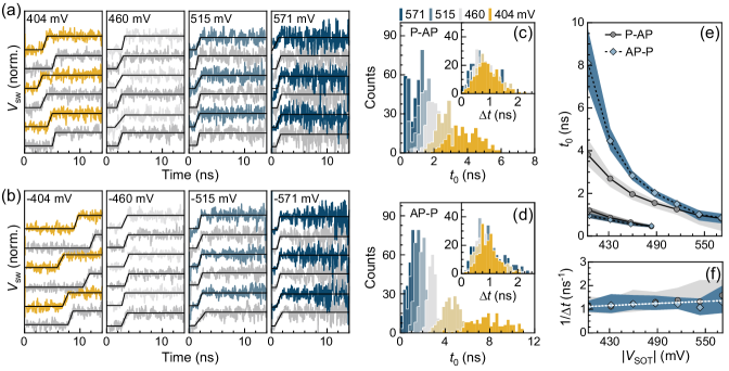
Figures 2(a) and 2(b) show representative time traces of individual P-AP and AP-P switching events obtained in zero external field for different pulse amplitudes of and , which corresponds to a current density of the critical STT switching current. The switching traces reveal that the reversal of the free layer starts after a finite incubation time () followed by a single jump of the resistance during a relatively short transition time (), after which the magnetization remains quiescent in the final state until the pulse ends. The reversal dynamics is thus qualitatively similar to that observed in the presence of an external magnetic field Grimaldi et al. (2020). Accordingly, we attribute to the time required to nucleate a reversed domain and to the time to propagate a domain wall across the free layer Grimaldi et al. (2020); Baumgartner et al. (2017). Noise in the time traces noticeably increases upon increasing and with the time elapsed from the pulse onset, which we associate with the rise of the device temperature during the pulse. Each reversal trace is fit by a linear ramp and the characteristic times and , defined in Fig. 1(d), are extracted from the line breakpoints. The distributions of and representing statistics over 200 single-shot measurements are plotted in Figs. 2(c) and 2(d). At low pulse amplitude, typical values of significantly exceed . However, both the center and the width of the distribution can be reduced by more than one order of magnitude by increasing .
To investigate the characteristic times in more detail, we extract the median as well as the lower and upper quartiles of each distribution and plot them as a function of . Figure 2(e) shows that the median decreases to below 1 ns for both AP-P and P-AP switching when increasing from 400 to 560 mV. At the lowest pulse amplitudes, the median of the AP-P switching configuration is twice as long compared to P-AP switching. This asymmetry, which is attributed to the dipolar field of the SAF, gradually reduces upon increasing . Additionally, our measurements show that such an asymmetry can be strengthened or eliminated by tuning . To demonstrate the potential of SOT-driven switching at increased , we report in the same plot obtained at (bottom curve). In this case, the difference between both configurations is minimized by VCMA, which favors AP-P at the expense of P-AP switching, whereas the median value and its dispersion are reduced by the bias-induced temperature rise in the device. Note that STT has the same hindering effect on both switching configurations, as it favors the orientation of the free layer opposite to the final state defined by . Moreover, despite the presence of a strong opposing STT when , which corresponds to of the critical STT switching current in the absence of SOT, we do not observe writing errors within our data set.
In contrast to , has a much weaker dependence on . Figure 2(f) shows that increases linearly with , with a moderate slope of 1.5 ns-1 V-1. Linear scaling with current is indeed expected for the speed of SOT-driven domain walls in the flow regime Miron et al. (2011b); Thiaville et al. (2012); Emori et al. (2013); Martinez et al. (2013). Supposing that the reversal initiates with the nucleation of a domain wall at one edge of the free layer, as shown in previous work Mikuszeit et al. (2015); Baumgartner et al. (2017), our data imply an average domain-wall propagation speed of 100 m s-1 induced by an SOT current density of A m-2 at = 0.48 V.
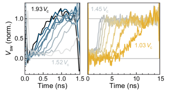
To demonstrate the reliability of switching for repeated events, we performed time-resolved measurements averaged over 1000 switching trials, as shown in Fig. 3. Averaging the acquired waveforms allows us to decrease the bias down to , which corresponds to a current density that is % of the STT switching threshold. The time traces compare AP-P switching for different values of given in multiples of the critical switching voltage (), corresponding to 50% switching probability. Each trace comprises an initial delay and a smooth transition part without noticeable intermediate states. Shortening of the delay and transition part of the averaged time traces indicates that the switching process changes from stochastic to almost deterministic upon increasing . We further observe a striking reduction of the total switching time from 15 ns to less than 1 ns at , which can be interpreted as switching at sub-ns timescale in the great majority of the 1000 trials, with the confidence given by the signal-to-noise ratio.
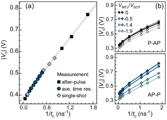
Our measurements also allow us to compare the critical switching voltage obtained by after-pulse, single-shot, and averaged time-resolved measurements. This comparison is relevant to assess the reliability of different methods employed to measure , particularly for the more common after-pulse resistance measurements, in which or cannot be accessed. We define the critical switching time () as the pulse width corresponding to 50% switching probability in after-pulse measurements, and as and the time required to reach = 0.5, in single-shot and averaged time-resolved measurements, respectively. Likewise, we define as the corresponding SOT pulse amplitude. Figure 4(a) shows that, irrespective of the measurement method, all values of fall on the same curve and scale inversely with the critical time for pulses shorter than 4 ns. Such a scaling is expected for the intrinsic regime, in which conservation of angular momentum gives Bedau et al. (2010); Liu et al. (2014); Garello et al. (2014). Here is the intrinsic critical voltage that reflects the minimum amount of angular momentum required to achieve switching in the absence of thermal effects. A linear fit of the data in Fig. 4(a) gives = 390 mV, which corresponds to an intrinsic critical current of A m-2. For pulses longer than 4 ns, deviations from the linear behavior are attributed to the onset of thermally-activated switching Bedau et al. (2010); Liu et al. (2014); Garello et al. (2014).
Figure 4(b) shows that in both switching configurations, reduces considerably upon increasing . The reduction of is largest for the shorter pulses and for AP-P switching (bottom panel) compared to P-AP switching (top panel). These observations can be explained by the combined impact of VCMA and heat generated by the bias. facilitates switching by weakening the anisotropy of the free layer, whereas the bias current simultaneously increases the temperature in the device, thus lowering the switching energy barrier regardless of its sign. Therefore, when is negative (AP-P switching), both VCMA and temperature lead to a reduction of ; however, when is positive (P-AP switching), the VCMA opposes the temperature-induced decrease of the switching barrier, resulting in a smaller reduction of . Consequently, in both switching configurations equalizes for . This result shows that can be efficiently used to realize symmetric switching conditions [see also Fig. 2(e)].
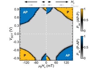
Last, we address the functionality of our devices under an external field () by measuring the after-pulse switching probability () for different pulse amplitude and field conditions. We start by considering SOT switching at = 0. Each point in the switching phase diagram in Fig. 5 illustrates the statistical result of 50 trials for a fixed pulse width (0.5 ns). The black boundary defines = 0.5, which divides the diagrams into under- (gray) and over-critical (blue and yellow) regions. Since polarizes the MHM, which has a coercivity of about 20 mT, is always antiparallel to [Fig. 1(a)]. As a consequence, the switching polarity depends on the sign of , i.e., of the total in-plane field acting on the free layer. The diagram also allows for evaluating the strength of from the difference between two values resulting in the same . In this manner, we estimate that mT. The diagram shows that bipolar switching is possible in a wide range of external fields with the exception of narrow intervals, in which approaches zero. A typical transition of from 0.01 to 0.99 occurs upon increasing by less than 80 mV, in contrast with STT switching, for which a 150 mV increase of is required using the same device and 15 ns-long pulses.
Before concluding, we discuss a few possibilities to improve the switching speed and the design of field-free SOT devices. As shown in Ref. Grimaldi et al., 2020, increasing the magnitude of the in-plane field significantly reduces the switching time for a given . In general, can be increased by i) optimizing the aspect ratio and thickness of the magnetic layer, ii) replacing the Co layer by a material with higher saturation magnetization, such as CoFe, and iii) bringing the MHM closer to the MTJ. The optimal strength of will ultimately depend on the critical current, switching rate, and thermal stability of the free layer set by the target application. Static measurements show that the TMR is not affected by the MHM and that the overall device properties are more influenced by the design of the MTJ pillar rather than by the hard mask itself Garello et al. (2019). Better compensation of the out-of-plane stray field produced by the SAF would lead to a more symmetric switching behavior between the P and AP configurations. This can be achieved, e.g., by changing the thickness of the reference layer or the thickness and number of repetitions of the SAF multilayer. Alternatively, as shown here, can be used to balance the SAF field. The MHM approach is also compatible with dense designs, as shown in Ref. Garello et al., 2019. Micromagnetic simulations further show that surrounding magnets have a stabilizing effect on the magnetization of the hard mask. MHMs down-scaled to a volume of nm3 and a pitch of nm2 have more uniform magnetization patterns than MHMs with a volume of nm3 and a pitch of nm2. Future studies might establish if the MHM approach based on a single mask per MTJ is compatible with sharing the same SOT write line between multiple MTJs, as proposed in Ref. Kato et al., 2018.
In summary, we have demonstrated field-free switching of perpendicularly magnetized MTJs by SOT in real time. Single-shot time-resolved measurements show that the stochastic incubation delay near the critical voltage threshold () is several ns long for both the AP-P and P-AP switching configurations, whereas the actual transition time is about 1 ns. Upon increasing or , the switching distributions narrow down leading to reduced latency and quasi-deterministic switching. Averaged time-resolved measurements show that the total switching time can be reduced to 0.7 ns by increasing up to with negligible assistance of either STT or VCMA. At timescales shorter than 4 ns, the critical switching voltage is found to scale linearly with inverse of the switching time, as expected in the intrinsic regime. Real-time measurements and after-pulse switching statistics as a function of pulse length are found to provide a consistent estimate of the critical switching time. Measurements of the switching probability as a function of and external field indicate that further improvements of the switching dynamics and reduction of can be obtained by VCMA, increase of the dipolar field of the MHM, and compensating the dipolar field due to the SAF.
This research was supported by the Swiss National Science Foundation (Grant no. 200020-172775), the Swiss Government Excellence Scholarship (ESKAS-Nr. 2018.0056), the ETH Zurich (Career Seed Grant SEED-14 16-2) and imec’s Industrial Affiliation Program on MRAM devices.
This article may be downloaded for personal use only. Any other use requires prior permission of the author and AIP Publishing. This article appeared in Appl. Phys. Lett. 116, 232406 (2020) and may be found at https://doi.org/10.1063/5.0011433.
References
- Manchon et al. (2019) A. Manchon, J. Železný, I. M. Miron, T. Jungwirth, J. Sinova, A. Thiaville, K. Garello, and P. Gambardella, Rev. Mod. Phys. 91, 035004 (2019).
- Miron et al. (2011a) I. M. Miron, K. Garello, G. Gaudin, P. J. Zermatten, M. V. Costache, S. Auffret, S. Bandiera, B. Rodmacq, A. Schuhl, and P. Gambardella, Nature 476, 189 (2011a).
- Liu et al. (2012) L. Liu, C.-F. Pai, Y. Li, H. W. Tseng, D. C. Ralph, and R. A. Buhrman, Science 336, 555 (2012).
- Cubukcu et al. (2014) M. Cubukcu, O. Boulle, M. Drouard, K. Garello, C. Onur Avci, I. Mihai Miron, J. Langer, B. Ocker, P. Gambardella, and G. Gaudin, Appl. Phys. Lett. 104, 042406 (2014).
- Fukami et al. (2016a) S. Fukami, T. Anekawa, C. Zhang, and H. Ohno, Nat. Nanotechnol. 11, 621 (2016a).
- Lee and Lee (2016) S. W. Lee and K. J. Lee, Proc. IEEE 104, 1831 (2016).
- Luo et al. (2020) Z. Luo, A. Hrabec, T. P. Dao, G. Sala, S. Finizio, J. Feng, S. Mayr, J. Raabe, P. Gambardella, and L. J. Heyderman, Nature 579, 214 (2020).
- Garello et al. (2014) K. Garello, C. O. Avci, I. M. Miron, M. Baumgartner, A. Ghosh, S. Auffret, O. Boulle, G. Gaudin, and P. Gambardella, Appl. Phys. Lett. 105, 212402 (2014).
- Zhang et al. (2015) C. Zhang, S. Fukami, H. Sato, F. Matsukura, and H. Ohno, Appl. Phys. Lett. 107, 1 (2015).
- Aradhya et al. (2016) S. V. Aradhya, G. E. Rowlands, J. Oh, D. C. Ralph, and R. A. Buhrman, Nano Lett. 16, 5987 (2016).
- Baumgartner et al. (2017) M. Baumgartner, K. Garello, J. Mendil, C. O. Avci, E. Grimaldi, C. Murer, J. Feng, M. Gabureac, C. Stamm, Y. Acremann, S. Finizio, S. Wintz, J. Raabe, and P. Gambardella, Nat. Nanotechnol. 12, 980 (2017).
- Yoon et al. (2017) J. Yoon, S. W. Lee, J. H. Kwon, J. M. Lee, J. Son, X. Qiu, K. J. Lee, and H. Yang, Sci. Adv. 3, e1603099 (2017).
- Decker et al. (2017) M. M. Decker, M. S. Wörnle, A. Meisinger, M. Vogel, H. S. Körner, G. Y. Shi, C. Song, M. Kronseder, and C. H. Back, Phys. Rev. Lett. 118, 257201 (2017).
- Cubukcu et al. (2018) M. Cubukcu, O. Boulle, N. Mikuszeit, C. Hamelin, T. Brächer, N. Lamard, M.-C. Cyrille, L. Buda-Prejbeanu, K. Garello, I. M. Miron, O. Klein, G. D. Loubens, V. V. Naletov, J. Langer, B. Ocker, P. Gambardella, and G. Gaudin, IEEE Trans. Magn. 54, 9300204 (2018).
- Kato et al. (2018) Y. Kato, Y. Saito, H. Yoda, T. Inokuchi, S. Shirotori, N. Shimomura, S. Oikawa, A. Tiwari, M. Ishikawa, M. Shimizu, B. Altansargai, H. Sugiyama, K. Koi, Y. Ohsawa, and A. Kurobe, Phys. Rev. Appl. 10, 044011 (2018).
- Grimaldi et al. (2020) E. Grimaldi, V. Krizakova, G. Sala, F. Yasin, S. Couet, G. S. Kar, K. Garello, and P. Gambardella, Nat. Nanotechnol. 15, 111 (2020).
- Kent and Worledge (2015) A. D. Kent and D. C. Worledge, Nat. Nanotechnol. 10, 187 (2015).
- Apalkov, Dieny, and Slaughter (2016) D. Apalkov, B. Dieny, and J. M. Slaughter, Proc. IEEE 104, 1796 (2016).
- Prenat et al. (2016) G. Prenat, K. Jabeur, P. Vanhauwaert, G. D. Pendina, F. Oboril, R. Bishnoi, M. Ebrahimi, N. Lamard, O. Boulle, K. Garello, J. Langer, B. Ocker, M. C. Cyrille, P. Gambardella, M. Tahoori, and G. Gaudin, IEEE Trans. Multi-Scale Comput. Syst. 2, 49 (2016).
- Fukami et al. (2016b) S. Fukami, C. Zhang, S. Duttagupta, A. Kurenkov, and H. Ohno, Nat. Mater. 15, 535 (2016b).
- Oh et al. (2016) Y. W. Oh, S. H. C. Baek, Y. M. Kim, H. Y. Lee, K. D. Lee, C. G. Yang, E. S. Park, K. S. Lee, K. W. Kim, G. Go, J. R. Jeong, B. C. Min, H. W. Lee, K. J. Lee, and B. G. Park, Nat. Nanotechnol. 11, 878 (2016).
- van den Brink et al. (2016) A. van den Brink, G. Vermijs, A. Solignac, J. Koo, J. T. Kohlhepp, H. J. Swagten, and B. Koopmans, Nat. Commun. 7, 10854 (2016).
- Lau et al. (2016) Y. C. Lau, D. Betto, K. Rode, J. M. Coey, and P. Stamenov, Nat. Nanotechnol. 11, 758 (2016).
- Luo et al. (2019) Z. Luo, T. P. Dao, A. Hrabec, J. Vijayakumar, A. Kleibert, M. Baumgartner, E. Kirk, J. Cui, T. Savchenko, G. Krishnaswamy, L. J. Heyderman, and P. Gambardella, Science 363, 1435 (2019).
- You et al. (2015) L. You, O. J. Lee, D. Bhowmik, D. Labanowski, J. Hong, J. Bokor, and S. Salahuddin, Proc. Natl. Acad. Sci. U. S. A. 112, 10310 (2015).
- Yu et al. (2014) G. Yu, P. Upadhyaya, Y. Fan, J. G. Alzate, W. Jiang, K. L. Wong, S. Takei, S. A. Bender, L. T. Chang, Y. Jiang, M. Lang, J. Tang, Y. Wang, Y. Tserkovnyak, P. K. Amiri, and K. L. Wang, Nat. Nanotechnol. 9, 548 (2014).
- Safeer et al. (2016) C. K. Safeer, E. Jué, A. Lopez, L. Buda-Prejbeanu, S. Auffret, S. Pizzini, O. Boulle, I. M. Miron, and G. Gaudin, Nat. Nanotechnol. 11, 143 (2016).
- Chen et al. (2018) T. Y. Chen, H. I. Chan, W. B. Liao, and C. F. Pai, Phys. Rev. Appl. 10, 044038 (2018).
- van den Brink et al. (2014) A. van den Brink, S. Cosemans, S. Cornelissen, M. Manfrini, A. Vaysset, W. Van Roy, T. Min, H. J. Swagten, and B. Koopmans, Appl. Phys. Lett. 104, 012403 (2014).
- Wang et al. (2018) M. Wang, W. Cai, D. Zhu, J. Kan, Z. Zhao, K. Cao, Z. Wang, Z. Wang, Y. Zhang, T. Zhang, C. Park, J.-P. Wang, A. Fert, and W. Zhao, Nat. Electron. 1, 582 (2018).
- de Orio et al. (2019) R. L. de Orio, A. Makarov, S. Selberherr, W. Goes, J. Ender, S. Fiorentini, and V. Sverdlov, Solid State Electron. 168, 107730 (2019).
- Garello et al. (2019) K. Garello, F. Yasin, H. Hody, S. Couet, L. Souriau, S. H. Sharifi, J. Swerts, R. Carpenter, S. Rao, W. Kim, J. Wu, K. Sethu, M. Pak, N. Jossart, D. Crotti, A. Furnemont, and G. S. Kar, IEEE Symp. VLSI Technol. , T194 (2019).
- Devolder et al. (2008) T. Devolder, J. Hayakawa, K. Ito, H. Takahashi, S. Ikeda, P. Crozat, N. Zerounian, J. V. Kim, C. Chappert, and H. Ohno, Phys. Rev. Lett. 100, 057206 (2008).
- Tomita et al. (2008) H. Tomita, K. Konishi, T. Nozaki, H. Kubota, A. Fukushima, K. Yakushiji, S. Yuasa, T. Shinjo, Y. Nakatani, M. Shiraishi, and Y. Suzuki, Appl. Phys. Express 1, 061303 (2008).
- Cui et al. (2010) Y.-T. Cui, G. Finocchio, C. Wang, J. A. Katine, R. A. Buhrman, and D. C. Ralph, Phys. Rev. Lett. 104, 097201 (2010).
- Hahn et al. (2016) C. Hahn, G. Wolf, B. Kardasz, S. Watts, M. Pinarbasi, and A. D. Kent, Phys. Rev. B 94, 214432 (2016).
- Devolder, Le Goff, and Nikitin (2016) T. Devolder, A. Le Goff, and V. Nikitin, Phys. Rev. B 93, 224432 (2016).
- Devolder et al. (2016) T. Devolder, J. V. Kim, F. Garcia-Sanchez, J. Swerts, W. Kim, S. Couet, G. Kar, and A. Furnemont, Phys. Rev. B 93, 024420 (2016).
- Inokuchi et al. (2019) T. Inokuchi, H. Yoda, K. Koi, N. Shimomura, Y. Ohsawa, Y. Kato, S. Shirotori, M. Shimizu, H. Sugiyama, S. Oikawa, B. Altansargai, and A. Kurobe, Appl. Phys. Lett. 114, 192404 (2019).
- Miron et al. (2011b) I. M. Miron, T. Moore, H. Szambolics, L. D. Buda-prejbeanu, S. Auffret, B. Rodmacq, S. Pizzini, J. Vogel, M. Bonfim, A. Schuhl, and G. Gaudin, Nat. Mater. 10, 419 (2011b).
- Thiaville et al. (2012) A. Thiaville, S. Rohart, É. Jué, V. Cros, and A. Fert, Europhys. Lett. 100, 57002 (2012).
- Emori et al. (2013) S. Emori, U. Bauer, S.-M. Ahn, E. Martinez, and G. S. D. Beach, Nat. Mater. 12, 611 (2013).
- Martinez et al. (2013) E. Martinez, S. Emori, G. S. D. Beach, E. Martinez, S. Emori, and G. S. D. Beach, Appl. Phys. Lett. 103, 072406 (2013).
- Mikuszeit et al. (2015) N. Mikuszeit, O. Boulle, I. M. Miron, K. Garello, P. Gambardella, G. Gaudin, and L. D. Buda-Prejbeanu, Phys. Rev. B 92, 144424 (2015).
- Bedau et al. (2010) D. Bedau, H. Liu, J. Z. Sun, J. A. Katine, E. E. Fullerton, S. Mangin, and A. D. Kent, Appl. Phys. Lett. 97, 262502 (2010).
- Liu et al. (2014) H. Liu, D. Bedau, J. Z. Sun, S. Mangin, E. E. Fullerton, J. A. Katine, and A. D. Kent, J. Magn. Magn. Mater. 358-359, 233 (2014).