Fingerprinting Analog IoT Sensors for
Secret-Free Authentication
Abstract
Especially in context of critical urban infrastructures, trust in IoT data is of utmost importance. While most technology stacks provide means for authentication and encryption of device-to-cloud traffic, there are currently no mechanisms to rule out physical tampering with an IoT device’s sensors. Addressing this gap, we introduce a new method for extracting a hardware fingerprint of an IoT sensor which can be used for secret-free authentication. By comparing the fingerprint against reference measurements recorded prior to deployment, we can tell whether the sensing hardware connected to the IoT device has been changed by environmental effects or with malicious intent. Our approach exploits the characteristic behavior of analog circuits, which is revealed by applying a fixed-frequency alternating current to the sensor, while recording its output voltage. To demonstrate the general feasibility of our method, we apply it to four commercially available temperature sensors using laboratory equipment and evaluate the accuracy. The results indicate that with a sensible configuration of the two hyperparameters we can identify individual sensors with high probability, using only a few recordings from the target device.
Index Terms:
Internet of Things, Trust, Secret-Free Authentication, Fingerprinting, IC Identification, Analog SensorsI Introduction
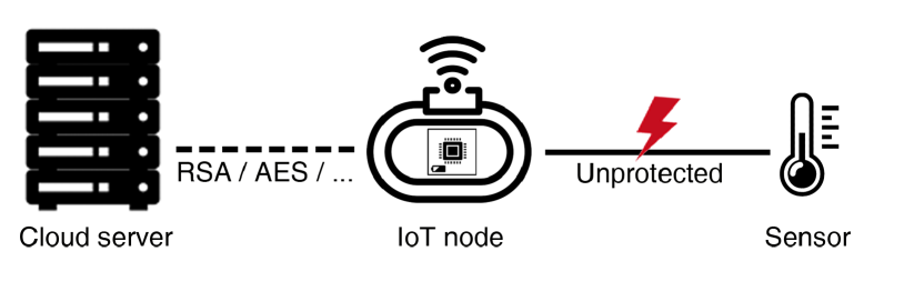
Internet of Things (IoT) technology provides a promising path towards improved monitoring and control of critical urban infrastructures such as transport systems, water networks, and telemedicine systems [1]. With the stringent security requirements of these application domains, reliable means to establish trust in the sensor data streams is of absolute necessity. Established cryptographic protocols can be used to protect the data from malicious third parties while it traverses the fog. However, in many cases IoT nodes are situated in physically vulnerable, publicly accessible spots, where attackers can gain access to a device and tamper with its peripherals. In other words, even if a device’s identity has been established and is therefore trustworthy, how can we verify that the signals coming from its sensors are trustworthy as well? In the literature, this problem is called sensor-crypto separation [2] and generally refers to the possibility of intercepting signals between an analog sensing device and the IC processing the results.
In this paper, we address the problem of sensor-crypto separation with a novel method for fingerprinting the sensors connected to an IoT node. Our method is based on the application of alternating currents to the sensor inputs and reading the sensor outputs. Before deployment of a sensor-equipped device, a broad frequency spectrum is scanned and the results are stored in a database. Later, when a device wants to prove that its sensing hardware has not changed, it transmits the responses to a small set of probe frequencies. The remote party can then compare the received responses with the ones in the database and, based on their deviation, decide whether the configuration is likely to have changed in-between deployment and the current response or not. Identification granularity can be divided into two categories:
-
•
Inter-device identification distinguishes between different sensor models.
-
•
Intra-device identification distinguishes between different instances of the same model.
Of course, the latter is more difficult than the former, and any method that can reliably distinguish between sensor instances can also distinguish models.
Using a set of commercial off-the-shelf (COTS) IoT sensors and standard laboratory equipment, we demonstrate the general feasibility of our approach and discuss its strengths and limitations.
We conclude that our method is powerful enough to perform inter- and intra-device identification with bounded error.
The rest of this paper is structured as follows: First, we introduce a few relevant concepts in Section II and discuss related publications in Section III. Then, we introduce our method in Section IV and evaluate it for several commercial IoT temperature sensors using precision measurement equipment in Section V. Finally, in Section VI we provide a discussion of the results, before we conclude the paper and highlight our plans for further improvements in Section VII.
II Background
The fingerprinting technique discussed in this paper relates to some concepts from the security domain, which are briefly introduced below.
Challenge-response authentication
Some of the fingerprinting techniques discussed in Section III are based on the challenge-response principle: To authenticate a device, the remote party sends a question (“challenge”) for which the local party must produce a valid answer (“response”). Before deployment, the system is bootstrapped, which means that for all possible challenges, the corresponding responses of the target system are recorded and stored. Later, checking the validity of any single response corresponds to a simple comparison with the database of challenge-response pairs. For reliable identification the device should consistently produce the same response to a given challenge and no two devices must produce identical responses to all available challenges). Hardware implementations of the challenge-response principle predominantly rely on process variation during manufacturing to ensure uniqueness.
Secret-free authentication
Cryptographic schemes often include the establishment of a shared secret between the involved parties that is used for authentication and encryption. Naturally, a wide range of attacks have been devised that focus on extracting the secret, e.g. using malware or through some physical side channel. To eliminate this class of attacks, researchers are trying to develop secret-free schemes, where everything about both ends of a conversation is known and yet an attacker has no way of impersonating one or the other party [3]. Current examples of secret-free authentication are presented in the next section.
III Related Work
Many IoT solutions rely on Low-Power Wide Area Network (LPWAN) technology for communication and the popular implementations support block cypher encryption between devices as well as application server. Therefore, the research community has primarily focused on identifying the type of node connected to a network based on the observed network traffic [4, 5, 6]. To the best of our knowledge, no works have been published that go beyond the end device to determine if its sensor configuration has changed. In the following sections, we revise fingerprinting methods that rely on similar physical characteristics as the one described in this paper, despite the fact that they were not specifically developed for IoT applications.
III-A (Public) Physical Unclonable Functions
Physical Unclonable Functions (PUFs) are special circuits designed to specify a device with a unique and unclonable identity for authentication. The circuit takes a bit pattern as input and deterministically produces another bit pattern as output. Process variations during manufacturing make the mapping between inputs and outputs unique and prevents an attacker vom physically duplicating the circuit. In the recent past, PUFs have fallen slightly out of favor due to their susceptibility to a class of attacks which use Machine Learning to simulate the PUF behavior [7].
This weakness was later addressed through the introduction of Public Physical Unclonable Functions (PPUFs) [8].
Everything about a PPUF’s circuit is public knowledge and yet the system is designed in a way that an attacker cannot simulate the device efficiently, i.e. simulating a response takes significantly longer than just physically producing it with the original circuit.
By verifying the timing of the response in addition to its correctness, the remote party can verify that it is dealing with the real device and not a simulation of it.
The PUF principle can be transferred to various kinds of materials that are also subject to process variation, such as CDs and sheets of paper [9].
In this case, the medium is called unique object (UNO) and the fingerprint is revealed using a high-resolution measurement device, such as a microscope.
UNOs and PPUFs constitute prime examples of secret-free cryptographic systems and are based on the same principle as our method:
To reveal unique properties of physical objects that result from process variations.
Both PUF and PPUF have been suggested as suitable technologies for authentication protocols in IoT ecosystems. In most cases, the circuit is directly integrated with the IoT node or added as a peripheral identification module. But there have also been efforts to combine a sensing circuit and a fingerprint circuit into a sensor that can do both at the same time: measuring a target observable and identifying itself. In [2] the authors propose to fuse a photosensor with a PUF to produce a device that signs each measurement with a response before it leaves the PUF circuit. Similar schemes have been described for measuring pressure [10] and voltage [11], and capacitance [12] respectively. Others go further and use the environment-dependent behavior of a PUF directly for sensing [13], albeit with serious limitations: While they prove that it is possible to detect faults injected into the devices power supply, it remains an open question whether the idea can be transferred to sensors for other physical quantities. Unfortunately, all approaches in which a sensor is directly combined with a PUF introduce dedicated circuits, which means they are incompatible with COTS sensors currently on the market. Our method addresses this gap by revealing the uniqueness of a sensor itself instead of relying on the entropy of a PUF circuit.
III-B Smartphone and Radio Fingerprinting
In the recently emerging field of smartphone fingerprinting, the goal is to identify a smartphone remotely with high probability by revealing the uniqueness of its internal sensors. One of the earliest methods was developed by Dey and colleagues [14] and aims to identify a phone via its built-in accelerometer. Specifically, the challenge is produced in the form of a vibration from the internal mechanical vibrator and consecutively, the response is captured as accelerometer readings. Inconveniently the success of their method depends on the surface on which the phone is laying. To overcome that limitation, another approach was soon proposed by Bojinov et al. [15]. Here, the challenge is emitted through the phone’s speakers in the form of an auditory signal and simultaneously recorded as a response using the microphone. Their method does not require the device to be in a specific physical location but still depends on a relatively noise-free environment in order to work properly. Finally, integrated schemes were described for combining the fingerprints of multiple sensors for more reliable identification [16, 17]. A comprehensive review of the literature on smartphone identification can be found in [18] as well as a discussion of relevant attacks in [19].
For devices without built-in sensors and actuators, physical-layer identification techniques focus on unique characteristics of the analog radio circuitry in wireless transceivers [20]. They are subsumed under the term RF-DNA and construct models of the device classes from the observed radio communication using methods like Wavelet transform [21] or Hilbert Huang transform [22].
IV Method
The main idea behind our fingerprinting method is to reveal the characteristic properties of a sensor’s analog circuit and use them for secret-free authentication: Due to the resistive, inductive, and capacitive parts, an analog circuit behaves like a harmonic oscillator upon being stimulated with alternating current (AC). The response is determined by the circuit’s layout, the attributes of individual electronic components, the frequency of the AC voltage, and environmental conditions such as air temperature or local magnetic field. Thus, assuming we can control or at least account for the influence of environmental factors, we can distinguish two sensors by comparing their responses to various input frequencies. The granularity of identification depends on the resolution of the measurement equipment, since the difference in behavior among circuit layouts is orders of magnitude larger than the difference due to process variation. It should also be noted that the characteristic behavior of the devices should be revealed at the operational limits of input parameters as specified in the datasheets. E.g. if a sensor’s operational voltage range is specified as 3.3V to 5V, we should test around 3.3V since going above 5V could damage the device. The intuition behind this is, that the circuits are designed with certain in-built tolerances and compensation mechanisms within the supported ranges that would conceal characteristic behavior.
IV-A Fingerprint Extraction
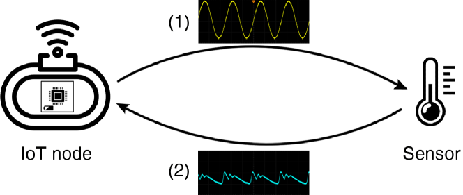
Our approach follows the challenge-response principle:
The sensor is supplied with an oscillating voltage of a fixed pattern and frequency (challenge).
Oscillation range and waveform are selected according to the capabilities of the available hardware.
Meanwhile, its output voltage is sampled for a certain number of steps and used to compute specific parameters of the output waveform (response).
In the following, we focus on effective value and variance but briefly discuss other options in Section VI.
Since the responses of two different sensors can happen to coincide for some frequencies, multiple such challenge-response pairs must be recorded to reduce the number of false positives.
A schematic representation of our method is given in Figure 2.
IV-B Authentication scheme
The fingerprinting method is used as part of an authentication scheme that proceeds similarly to how PUF-based authentication works. Prior to device deployment, a bootstrapping step is performed. This is essentially a sweep over a predefined frequency band with the responses for each point being recorded. The resulting set of challenge-response pairs is denoted as full fingerprint of the target device and must be kept secure with the trusted remote party. Depending on the IoT architecture and network topology, this might be a cloud server or an edge node. Then, the sensor is connected to an IoT node and deployed to its designated location. To authenticate the sensor in the field, first the corresponding IoT node is authenticated using a standard authentication mechanism. Then, a set of challenge frequencies called partial fingerprint is chosen according to a predefined pattern and the responses are sent to the backend for verification. Here, we deviate from the usual process of PUF-based authentication: In order to reduce communication overhead and conserve power of the IoT node, we do not transmit the challenge from the remote endpoint to the device but instead apply a hashing function locally to the current timestamp to obtain a set of input frequencies. If the partial fingerprint deviates from the responses of the full fingerprint by no more than a specified margin, we consider the authentication to be successful and can assume that the measurement originated from the same circuit that was bootstrapped previously.
V Preliminary Experiments
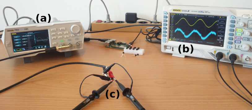
To verify the general feasibility of our approach, we conducted a series of experiments on real IoT sensors using laboratory equipment as presented in Figure 3.
Specifically, we use a Rigol DG812 function generator to produce the input oscillations and measure sensor output voltage with a Rigol DS1054Z oscilloscope.
The digital-to-analog converter (DAC) inside the function generator offers a resolution of 16 bits with a sampling rate of 125 MSa/s, whereas the oscilloscope’s analog-to-digital converter (ADC) has 8 bit resolution and a sampling rate of 1 GSa/s.
The transferability of the results to inexpensive, low-power IoT hardware is discussed in Section VI.
The sensors are listed in Table I and are all available in the TO-92 packaging.
The frequencies are taken from the range in 1 kHz steps, i.e. .
In this paper, we limit our considerations to computing the root mean square (RMS) (also called effective voltage) of the recorded output signal.
The RMS is an equivalent voltage which represents the DC voltage value that would produce the same heating effect, or power dissipation, in the circuit, as the applied AC voltage.
| TMP36 | LM61 | MCP9700 | LMT85 | |
| Min/max temp. (°C) | -40/+125 | -30/+100 | -40/+150 | -50/+150 |
| Accuracy (°C) | 2 | 2 | 1 | 0.7 |
| Min/max supply (V) | 2.7/5.5 | 2.7/10 | 2.3/5.5 | 1.8/5.5 |
| Supply current (A) | 50 | 125 | 6 | 5.4 |
| Manufacturer | AD | TI | Microchip | TI |
Our experiments shall give an insight on the granularity of identification that can be achieved using the proposed method: Inter-device identification aims to distinguish between two different circuit layouts, whereas intra-device identification relies on differences between identical circuit layouts due to process variation. The latter is of course the more difficult task, requiring more precise equipment and being less likely to succeed.
V-A Full Fingerprints
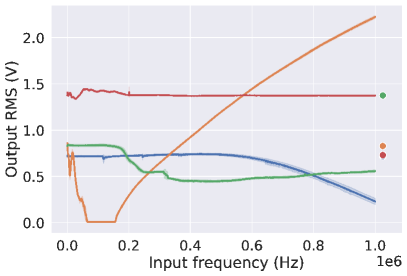
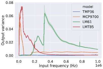
First, we qualitatively compare full fingerprints between different sensor models over the entire 1 MHz band. Figure 4 displays RMS and variance per 1 kHz step for the four tested models. Solid lines represent the average value over three independent measurements with approximately the same environmental temperature (). Shaded areas around the curves show the standard deviation . The dots in Figure 4a mark the measured output voltage of the sensors when supplied with 3.3V DC at room temperature. These values are identical for TMP36 and LMT85 so their points coincide. Visual inspection suggests that with the exception of a few crossing points, the differences between device models are large enough for reliable identification. Interestingly, the variance of TMP36 never exceeds , indicating exponentially increasing dynamic impedance. We also observe MCP9700 to entirely shut down for a certain band of frequencies around 100 kHz. This could be due to a high reactance but further analysis is needed since the datasheets are inconclusive in this regard.
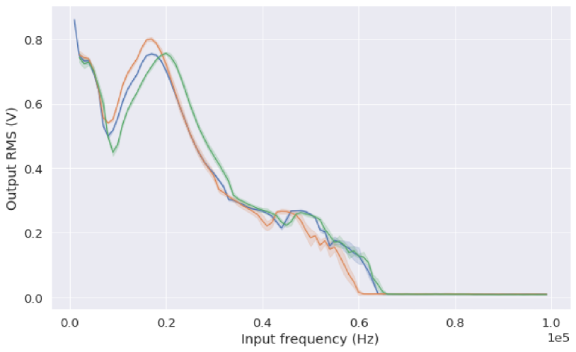
For intra-device variation, we take an exemplary look at the output RMS of three different instances of the MCP9700 sensor in Figure 5. The input domain (x axis) is narrowed to the first 100 kHz for increased readability. Again, solid lines correspond to mean values while shaded areas visualize the standard deviation w.r.t. multiple measurements of each device. Visual inspection reveals differences beyond the confidence intervals but quantitative analysis is needed before conclusions can be drawn.
V-B Sensor Identification
Following the authentication scheme presented above, we recall that a partial fingerprint is constructed from the RMS responses to a set of challenge frequencies. Authentication then proceeds by computing the deviation of the partial fingerprint from the previously obtained and stored full fingerprint. The root mean square error (RMSE), or identification error, is used to quantify the difference between a target partial fingerprint and the reference full fingerprint. For a given full fingerprint consisting of responses and a partial fingerprint with , we compute the RMSE as follows:
| (1) |
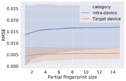
In PUF-based authentication, usually the hamming distance is used, because responses consist of bit sequences instead of a set of real numbers. It is reasonable to assume that the identification error decreases with an increasing number of points per partial fingerprint. We assess this assumption by showing mean RMSE values for different partial fingerprint sizes in in Figure 6a. In total, 1000 matchings between randomly chosen partial fingerprints and the corresponding full fingerprint were performed per device and partial fingerprint size. We only compare RMSE of target device matching with that of intra-device matching because the inter-device RMSE is orders of magnitude higher and would distort the graph significantly. The graph confirms that with larger number of points per partial fingerprint, the difference between intra-device RMSE and target device RMSE increases and thus the identification error decreases. Additionally, we observe the standard deviation of RMSE to be nearly constant across fingerprint sizes for matchings with the target device itself, whereas it decreases for intra-device comparisons. While the general implication seems to be “the more points per partial fingerprint, the better”, we have to keep in mind that this parameter is also subject to practical constraints, since larger fingerprints require more power to record and communicate.
Once the RMSE between partial and full fingerprint has been calculated for the target device, a decision needs to be made whether the device under scrutiny really is the expected one.
A straightforward approach is to define a threshold parameter and declare a given partial fingerprint to not match the corresponding full fingerprint if the RMSE lies above that threshold.
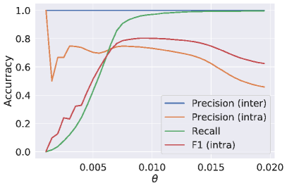
In Figure 6b, we investigate the relationship between fingerprinting accuracy and the threshold parameter .
Accuracy is operationalized as F1 score which is calculated from the classical information retrieval concepts precision and recall.
The resulting curves for and 10 points per partial fingerprint are displayed in Figure 6a.
As expected, recall improves for increasing up to a certain point because higher values correspond to a larger tolerance for deviations between partial and full fingerprint, e.g. due to noise.
With higher thresholds, the system would also accept fingerprints that differ due to process variation, resulting in an increasing number of intra-device false positives.
The best setting for under the tested conditions seems to be around where the F1 score is maximal.
Finally, in Table II, we report the number of false positives (FP) and false negatives (FN) per device and granularity for a fixed partial fingerprint size of 10 and . All numbers are given with respect to 1000 matchings. The results show that there is, on average, a 2.9% chance of a false mismatch with a fingerprint of the target device (false negative) over all four models. This residual error is probably connected to small fluctuations of the environmental temperature, which is further discussed in the next section. Just as with PUF authentication, in such a case, another authentication attempt could be initiated, reducing the probability for a false negative to . As for false positives, the results indicate we would never mistake another model for the target device, but multiple instances of the same model can be misclassified as false positives. This effect is less severe for some models, e.g. LM61 and very severe for others, e.g. LMT85. Looking again at Figure 4 we intuitively understand why this is the case: The full fingerprint of LMT85 has nearly constant RMS and very low variance for input frequencies above 200 kHz. Hence for this sensor, in practice, we should constrain the fingerprinting to regions of the spectrum, where intra-device variance of the target device is high in order to achieve good results.
| FN | FP (inter) | FP (intra) | |
|---|---|---|---|
| TMP36 | 6.5% | 0% | 1.7% |
| MCP9700 | 2.2% | 0% | 29.9% |
| LM61 | 1.3% | 0% | 0% |
| LMT85 | 1.5% | 0% | 94.3% |
VI Discussion of Practical Feasibility
Our results show that analog fingerprinting is a suitable method for both inter- and intra-device identification.
As indicated before, a few open questions have to be addressed before the approach can be used in critical IoT applications.
First, appropriate electrical components for generating the challenges (DAC) and reading the responses (ADC) have to be identified and tested.
The component properties must be balanced with respect to resolution, price and power consumption in order to be viable for large-scale deployments.
Currently, there are a number of candidate devices for such purposes on the market which will be tested in the next phase of our research.
In the same step, the accuracy of the approach could be improved by measuring the jitter curves of the ADC and DAC to account for their disturbance in the fingerprints.
Actually, we should account for the filter between DAC and sensor as well, which also has a significant influence on the quality of the input signal and thus on the reliability of the fingerprint.
It might also be possible to use chips as used for Impedance Spectroscopy (IS) which contain high precision DAC, ADC, and some additional circuits to compute high-level features such as Discrete Fourier Transform (DFT).
Likewise, the ADC could be replaced with an RMS-to-DC converter circuit to avoid recording multiple samples for manual RMS computation and thus save power.
Another critical question for the success of our method concerns the sensitivity of the device to changing environmental conditions.
That is, does the fingerprint change linearly with respect to the environmental temperature?
Many IoT temperature sensors, including the four devices under scrutiny in this paper, provide so-called linear slope characteristics within the specified operation temperature range111cf. e.g. https://www.analog.com/media/en/technical-documentation/data-sheets/TMP35_36_37.pdf.
The linearity is intended to allow for a first-order transfer function between measured voltage and sensed environmental temperature which simplifies device integration.
The reason why this is important for us is that during bootstrapping of the full fingerprints, the ambient temperature is very likely to differ from when the partial fingerprint is recorded.
Recall that in our experiments, this difference was controlled within .
However, if the effects on the fingerprint are linear, we can use efficient convex optimization methods to obtain a reliable fingerprint and at the same time determine the ambient temperature from the shift between partial and full fingerprint.
In other words, the fingerprint would implicitly contain the target observable, thus effectively fusing measurement with authentication.
Another solution would be to record multiple full fingerprints for different temperatures and use big data analysis methods to verify an incoming partial fingerprint.
Finally, IoT applications in critical infrastructures usually ensure fault tolerance through sensor redundancy, which could be exploited for cross-verification of individual fingerprints between co-located nodes.
VII Conclusion
In this paper, we presented a new method for fingerprinting sensors connected to an IoT node for secret-free authentication. The approach proceeds by challenging the device with a fixed-frequency alternating current, while observing the effective voltage at its outputs as the response. We tested four commercially available IoT temperature sensors using RMSE error to compute pairwise similarities between fingerprints. Our results show that the approach is, with bounded error, suitable for both inter- and intra-device identification. We further elaborated on the effects of two hyperparameters contained in our method, the size of a partial fingerprint and the threshold for the matching error. While the former is subject to a tradeoff between power consumption and accuracy, the latter balances false positives and false negatives. Next steps with our approach include the implementation using low-power IoT hardware and the integration of varying environmental conditions into our fingerprint model.
References
- [1] B. Rashid and M. H. Rehmani, “Applications of wireless sensor networks for urban areas: A survey,” Journal of network and computer applications, vol. 60, 2016.
- [2] K. Rosenfeld, E. Gavas, and R. Karri, “Sensor physical unclonable functions,” in 2010 IEEE international symposium on hardware-oriented security and trust (HOST). IEEE, 2010.
- [3] U. Rührmair, “Towards secret-free security.” IACR Cryptology ePrint Archive, vol. 2019, 2019.
- [4] B. Bezawada, M. Bachani, J. Peterson, H. Shirazi, I. Ray, and I. Ray, “Iotsense: Behavioral fingerprinting of iot devices,” arXiv preprint arXiv:1804.03852, 2018.
- [5] S. Marchal, M. Miettinen, T. D. Nguyen, A.-R. Sadeghi, and N. Asokan, “Audi: Toward autonomous iot device-type identification using periodic communication,” IEEE Journal on Selected Areas in Communications, vol. 37, no. 6, 2019.
- [6] T. D. Nguyen, S. Marchal, M. Miettinen, H. Fereidooni, N. Asokan, and A.-R. Sadeghi, “Dïot: A federated self-learning anomaly detection system for iot,” in 2019 IEEE 39th International Conference on Distributed Computing Systems (ICDCS). IEEE, 2019.
- [7] U. Rührmair, F. Sehnke, J. Sölter, G. Dror, S. Devadas, and J. Schmidhuber, “Modeling attacks on physical unclonable functions,” in Proceedings of the 17th ACM conference on Computer and communications security, 2010.
- [8] N. Beckmann and M. Potkonjak, “Hardware-based public-key cryptography with public physically unclonable functions,” in International Workshop on Information Hiding. Springer, 2009.
- [9] U. Rührmair, S. Devadas, and F. Koushanfar, “Security based on physical unclonability and disorder,” in Introduction to Hardware Security and Trust. Springer, 2012.
- [10] J. Tang, R. Karri, and J. Rajendran, “Securing pressure measurements using sensorpufs,” in 2016 IEEE International Symposium on Circuits and Systems (ISCAS). IEEE, 2016.
- [11] Y. Gao, H. Ma, D. Abbott, and S. F. Al-Sarawi, “Puf sensor: Exploiting puf unreliability for secure wireless sensing,” IEEE Transactions on Circuits and Systems I: Regular Papers, vol. 64, no. 9, 2017.
- [12] C. B. Karuthedath and N. Schwesinger, “Unique and unclonable capacitive sensors,” IEEE Sensors Journal, vol. 18, no. 15, 2018.
- [13] K. Shimizu, T. Sugawara, and D. Suzuki, “Puf as a sensor,” in 2015 IEEE 4th Global Conference on Consumer Electronics (GCCE). IEEE, 2015.
- [14] S. Dey, N. Roy, W. Xu, R. R. Choudhury, and S. Nelakuditi, “Accelprint: Imperfections of accelerometers make smartphones trackable.” in NDSS, 2014.
- [15] H. Bojinov, Y. Michalevsky, G. Nakibly, and D. Boneh, “Mobile device identification via sensor fingerprinting,” arXiv preprint arXiv:1408.1416, 2014.
- [16] W.-H. Lee and R. B. Lee, “Multi-sensor authentication to improve smartphone security,” in 2015 International Conference on Information Systems Security and Privacy (ICISSP). IEEE, 2015.
- [17] I. Amerini, R. Becarelli, R. Caldelli, A. Melani, and M. Niccolai, “Smartphone fingerprinting combining features of on-board sensors,” IEEE Transactions on Information Forensics and Security, vol. 12, no. 10, 2017.
- [18] G. Baldini and G. Steri, “A survey of techniques for the identification of mobile phones using the physical fingerprints of the built-in components,” IEEE Communications Surveys & Tutorials, vol. 19, no. 3, 2017.
- [19] K. Ren, Z. Qin, and Z. Ba, “Toward hardware-rooted smartphone authentication,” IEEE Wireless Communications, vol. 26, no. 1, 2019.
- [20] B. Danev, D. Zanetti, and S. Capkun, “On physical-layer identification of wireless devices,” ACM Computing Surveys (CSUR), vol. 45, no. 1, 2012.
- [21] R. W. Klein, M. A. Temple, and M. J. Mendenhall, “Application of wavelet-based rf fingerprinting to enhance wireless network security,” Journal of Communications and Networks, vol. 11, no. 6, 2009.
- [22] W. E. Cobb, E. D. Laspe, R. O. Baldwin, M. A. Temple, and Y. C. Kim, “Intrinsic physical-layer authentication of integrated circuits,” IEEE Transactions on Information Forensics and Security, vol. 7, no. 1, 2011.