Exciton diffusion and annihilation in nanophotonic Purcell landscapes
Abstract
Excitons spread through diffusion and interact through exciton-exciton annihilation. Nanophotonics can counteract the resulting decrease in light emission. However, conventional enhancement treats emitters as immobile and non-interacting. It neglects exciton redistribution between regions with different enhancements and the increase in non-radiative decay at high exciton densities. Here, we go beyond the localized Purcell effect to exploit exciton dynamics and turn their typically detrimental impact into additional emission. As interacting excitons diffuse through optical hotspots, the balance of excitonic and nanophotonic properties leads to either enhanced or suppressed photoluminescence. We identify the dominant enhancement mechanisms in the limits of high and low diffusion and annihilation. Diffusion lifts the requirement of spatial overlap between excitation and emission enhancements, which we harness to maximize emission from highly diffusive excitons. In the presence of annihilation, we predict improved enhancement at increasing powers in nanophotonic systems dominated by emission enhancement. Our guidelines are relevant for efficient and high-power light-emitting diodes and lasers tailored to the rich dynamics of excitonic materials such as monolayer semiconductors, perovskites, or organic crystals.
keywords:
Exciton transport; Exciton-exciton annihilation; Purcell effect; Mie resonances; Plasmonic resonances; Nanoparticle arraysMOE Key Laboratory of Modern Optical Technologies and Jiangsu Key Laboratory of Advanced Optical Manufacturing Technologies, School of Optoelectronic Science and Engineering, Soochow University, Suzhou 215006, China
1 Introduction
Nanophotonics can improve light emission by enhancing excitation and radiative rates, and beaming radiation 1, 2, 3, 4, 5, 6, 7, 8, 9, 10, 11, 12, 13. In the conventional Purcell effect, emitters such as molecules and quantum dots are treated as localized point dipoles 14, 15. Total enhancement thus benefits from the product of excitation and emission at a point, which guides the design of nanoresonators and metamaterials made of metals and dielectrics.
For excitonic emitters, however, the picture of emission arising from non-interacting dipoles at fixed positions is incomplete. In a variety of semiconductors, excitons are mobile and spread to large diffusion lengths compared to nanophotonic scales (10 – 500 nm). Examples include perovskites (diffusion length 100 – 1000 nm) 16, 17, 18, monolayer transition metal dichalcogenides (hundreds of nm) 19, 20, quantum dots (tens of nm) 21, 22, organic crystals (1 – 100 nm for singlet excitons, 10 – 1000 nm for triplets) 23, and carbon nanotubes (hundreds of nm) 24, 25. As a result, excitons can emit far from the intense near field where they originate, affecting their radiative rate. Additionally, diffusion deteriorates emission as emitters approach defects and boundaries, where they might decay non-radiatively 26, 27, 28, 29. A photonic modification of the radiative decay rate could decrease the effective diffusion length, thus improving performance.
Another important aspect of exciton dynamics is exciton-exciton annihilation 30, 25, 31. At high exciton densities, this nonlinear process contributes to and even dominates non-radiative losses, degrading the performance of light-emitting devices at high powers 32, 33 and potentially preventing lasing. Annihilation thus curtails the advantages of nanophotonic intensity enhancement as well by simultaneously increasing non-radiative decay.
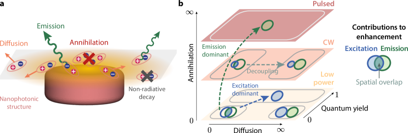
Here, we analyze the interplay of exciton dynamics and nanophotonic enhancement for thin films of excitonic emitters in nanostructured landscapes. We provide analytical results for enhancement under limiting cases of exciton dynamics. We demonstrate that, although diffusion and annihilation typically impede nanophotonic enhancement, it is possible to design nanostructures to overcome the lost efficiency. Diffusion can increase photoluminescence by taking excitons to highly radiative locations when excitation and emission are spatially decoupled. Radiative rate enhancement can ameliorate the loss of efficiency arising from annihilation, while the interplay between annihilation and diffusion can improve performance by redistributing the local exciton density. In summary, a careful balance of the relative strengths and spatial overlap of excitation and emission enhancements is the key to efficient excitonic-nanophotonic systems. Our guidelines for tailoring nanophotonic structures to diffusing and annihilating excitons will aid the design of efficient light-emitting devices.
2 Results
2.1 Exciton dynamics and nanophotonic enhancement
Excitons evolve in nanophotonic environments under the combined influence of incident intensity, radiative enhancement, non-radiative decay, diffusion, and annihilation (Figure 1a). We consider excitonic emitters in ultrathin films on top of nanodisk arrays with a negligible variation of electromagnetic fields across the film thickness. The two-dimensional exciton density evolves according to the exciton dynamics equation 20:
where is the exciton density at point at time , is the nanophotonically enhanced local excitation intensity at , is the absorption coefficient, is the spatially varying radiative decay rate, is the intrinsic non-radiative decay rate, is the diffusion constant, and is the annihilation constant. In the absence of nanophotonic structures, the intrinsic decay rates are and , where is the total decay rate and is the intrinsic quantum yield. The exciton decay time is and the diffusion length is . We assume that the nanostructures do not modify the non-radiative decay rate and the diffusion constant , although our model can incorporate such changes as well. We also neglect saturation of absorption at high power.
To compare systems with different excitonic and nanophotonic properties and extract the universal behavior of nanophotonic systems in the presence of exciton dynamics, we non-dimensionalize Equation (2.1). We identify physically relevant scales of exciton density, incident power, length, and time in the system to scale the variables , , , and with these values:
-
•
, where is the exciton density at which (the intrinsic total decay, which includes radiative and non-radiative rates but not annihilation) equals (the density-dependent annihilation),
-
•
, where is the incident continuous-wave power at which (the exciton generation) equals (the intrinsic decay at ),
-
•
, where is the period of the nanophotonic structures,
-
•
, where is the exciton decay time.
The characteristic scales depend on both excitonic and nanophotonic properties. Note that we perform scaling with respect to intrinsic properties (in the absence of nanostructures), except the length scale, which is the period of the array. Expressing Equation (2.1) in terms of the primed variables, we obtain the non-dimensionalized exciton dynamics equation
where and are the local nanophotonic excitation and radiative rate enhancements, and is the localized total decay rate enhancement. The non-dimensionalized diffusion constant is related to the diffusion length and the period of the nanophotonic structures by . The annihilation rate does not appear explicitly and is part of the characteristic incident power , demonstrating the utility of non-dimensionalization in comparing different systems. Excitonic materials that differ only in the annihilation rate will behave identically in a nanophotonic system except for scaling of incident power. We perform electromagnetic simulations using the surface integral equation (SIE) method and solve the non-dimensionalized exciton dynamics equation (2.1) to demonstrate the impact of exciton diffusion and annihilation on nanophotonic photoluminescence enhancement. We illustrate the diverse behavior and the possible scenarios of exciton dynamics using a variety of nanostructures.
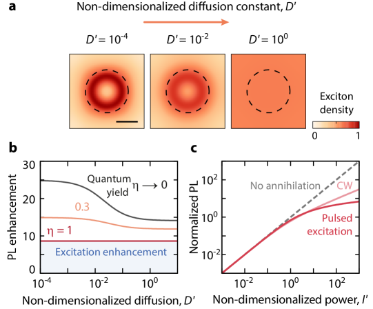
First, we analyze how diffusion affects it by spreading excitons out. We study excitonic emitters consisting of orientationally averaged dipoles above an array of silicon nanodisks. Although exciton density and diffusion are two-dimensional because the exciton film is thin, the exciton dipole moment can have components out of the plane – therefore, we average the orientations in all three dimensions 34. We assume perfect collection efficiency of the emission. We illuminate with a continuous-wave source at low power so that annihilation is initially negligible.
For low diffusion constants, the exciton density concentrates near the edge of the nanodisk, corresponding to the local excitation profile of an electric dipole in the nanodisk (Figure 2a). As the non-dimensionalized diffusion constant increases, the exciton density distribution expands, eventually becoming uniform over the unit cell. In this case, diffusion suppresses the total photoluminescence enhancement by taking excitons from regions of high radiative enhancement to positions of low enhancement (Figure 2b). The total photoluminescence is a combination of excitation and emission enhancements. Immobile emitters with low intrinsic quantum yield benefit from both excitation and emission enhancements, whereas only the increased excitation is relevant for emitters with high quantum yield 35, 36. The Purcell effect can be strongly modified upon diffusion, while the excitation is unaffected by diffusion in the absence of saturation effects. The impact of diffusion is the strongest for emitters with low quantum yield because of their larger contribution from radiative enhancement. For emitters with high intrinsic quantum yield, the Purcell effect enhances only the decay rate and not the photoluminescence. Diffusion reduces this enhancement (Supporting Figure S1a).
In the absence of nanostructures, exciton-exciton annihilation suppresses photoluminescence by opening an additional non-radiative channel at high excitation powers and exciton densities (Figure 2c). Compared to continuous-wave excitation, pulsed excitation creates higher instantaneous exciton densities, thereby reducing emission even further. Nanophotonic structures can ameliorate this deterioration of emission, as we shall discuss later. Additionally, the quick initial decay due to the high exciton density shortens the decay time considerably (Supporting Figure S1b).
2.2 Enhancing emission through diffusion
| Diffusion | Quantum yield | Incident power (with annihilation) | ||
|---|---|---|---|---|
| Continuous | Pulsed | |||
Generally, the deterioration of nanophotonic enhancement with diffusion is due to losing the advantage of spatial overlap between excitation and emission enhancements. To understand the contribution of each process and their overlap, we solve the non-dimensionalized exciton dynamics equation (2.1) analytically for limiting cases of quantum yield, diffusion, and annihilation (Supporting Section S1). We list the photoluminescence enhancement for these extremes in Table 1 and depict the contributions from excitation and emission and their overlap in Figure 1b, where the levels indicate the increasing role of annihilation. When the incident power is much lower than , annihilation is negligible compared to intrinsic decay (bottom level in Figure 1b). In this regime of negligible annihilation () and diffusion length much smaller than the period (), the total enhancement for emitters with poor efficiency () is , which is the spatial average of the product of local enhancements in the unit cell. Hence, in the absence of diffusion, we obtain high total enhancement if the excitation and emission significantly overlap.
In the regime of high diffusion, however, the total enhancement becomes , which is the product of the average values of excitation and emission in the unit cell. The spatial overlap of the enhancement factors is then no longer of benefit. As a result, the photoluminescence enhancement typically worsens with diffusion for low-efficiency emitters (Figure 3a). Although emitters with high quantum yield do not suffer a similar loss of enhancement because their emission efficiency does not change, their decay rate deteriorates with increasing diffusion (Figure 3a). Surprisingly, diffusion can modify the decay rate of emitters even in the limit of zero quantum yield (Supporting Figure S2).
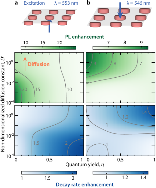
Diffusion can also improve emission by removing the spatial overlap between enhancement contributions. By controlling the excitation conditions such as the angle of incidence, polarization, or wavelength, we can lift the requirement of spatial overlap for maximum photoluminescence. As a first example, we spatially decouple excitation and emission by exploiting the angular pattern of emission in an array with a different geometry (Figure 3b and Supporting Figure S3). The excitation profile shows a strong front-back asymmetry because the high refractive index of silicon causes retardation of electromagnetic fields along its height 5. We illuminate the nanodisks from above to benefit from this asymmetry. The photoluminescence increases with diffusion at low , and so does the decay rate enhancement at high . Nanostructures designed under the assumption of immobile emitters can thus behave differently with diffusing excitons. Whether the impact of diffusion on enhancement is beneficial or detrimental depends on the nanophotonic system. Nanostructures aiming at maximum output from excitonic materials should thus take diffusion into account due to their spatially dependent enhancements 7, 4, 37, 38.
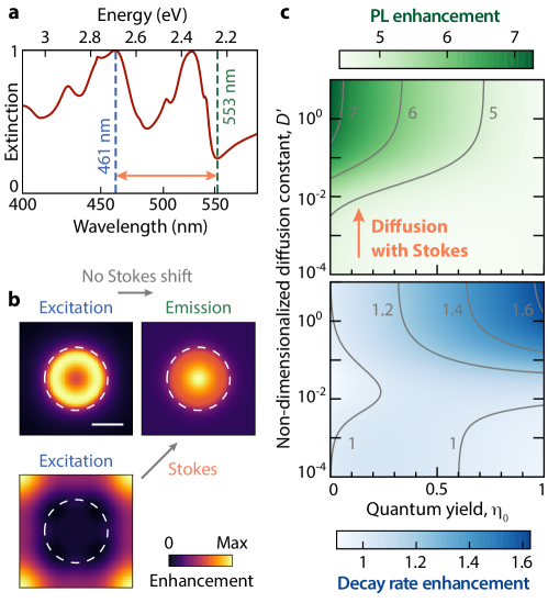
As a second case of enhancement through diffusion, we exploit the Stokes shift between excitation and emission wavelengths to decouple them spatially. We utilize the diversity of resonances supported by arrays of silicon nanodisks. (Figure 4a). For zero detuning with emission and excitation at = 553 nm, the excitation and radiative enhancements are both strongest above the disk (Figure 4b). The exciton density is highest near the edge because of the relatively high excitation enhancement there (Figure 2a). Due to the spatial overlap between enhancements, diffusion decreases photoluminescence as it transports excitons from regions of high excitation to areas of low radiative enhancements (Figure 3a). However, if the excitonic material has a Stokes shift between excitation at = 461 and emission at = 553 nm, the excitation enhancement is almost completely decoupled from the emission enhancement (Figure 4b). Diffusion thus takes the excitons generated at to regions of high radiative enhancement at , improving photoluminescence and decay rate compared to immobile excitons (Figure 4c). Emitters typically have a Stokes shift between excitation and emission, giving us a handle to turn diffusion to our advantage.
2.3 Overcoming annihilation through nanophotonic enhancement
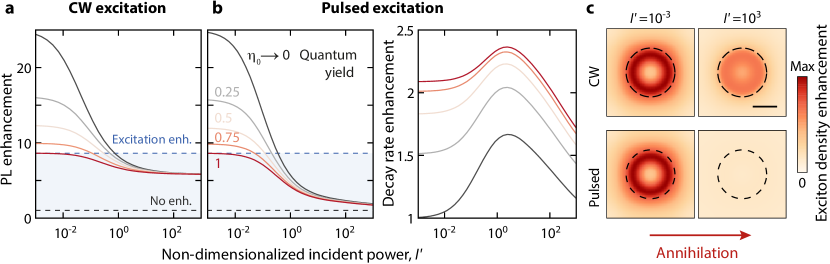
So far, we have only considered the effects of diffusion on nanophotonic enhancement. Next, we add exciton-exciton annihilation, which typically suppresses photoluminescence. As the incident power of a continuous-wave source increases, photoluminescence enhancement usually decreases for all quantum yields in the absence of diffusion (Figure 5a for the array in Figure 3a). At high power, the total nanophotonic enhancement falls even below the excitation enhancement (blue line). Exciton-exciton annihilation increases nonlinearly with power, suppressing the effect of excitation enhancement and reducing the steady-state exciton density enhancement (Figure 5c). At low power, the photoluminescence enhancement is due to for high- emitters, whereas it arises from the product of and for low- emitters. In contrast, at high power, the photoluminescence enhancement is the product of and independent of the quantum yield because exciton-exciton annihilation becomes the dominant non-radiative decay channel (Table 1).
The suppression of photoluminescence is even stronger for pulsed excitation (Figure 5b), where annihilation neutralizes the excitation enhancement completely as manifest in the time-averaged exciton density (Figure 5c). The emission enhancement still results in increased photoluminescence compared to the bare emitters. Exciton density enhancement on the nanostructure modifies the total decay rate via exciton-exciton annihilation, although the effect is neutralized once again at very high incident power (Figure 5b).
Diffusion can alleviate part of the detrimental effects of annihilation by smearing the hotspots of exciton density. Although emitters with high intrinsic quantum yield have diffusion-independent photoluminescence enhancement at low incident power (Figure 4c), the drop in enhancement with increasing power is much slower for highly diffusing excitons (Figure 6a).
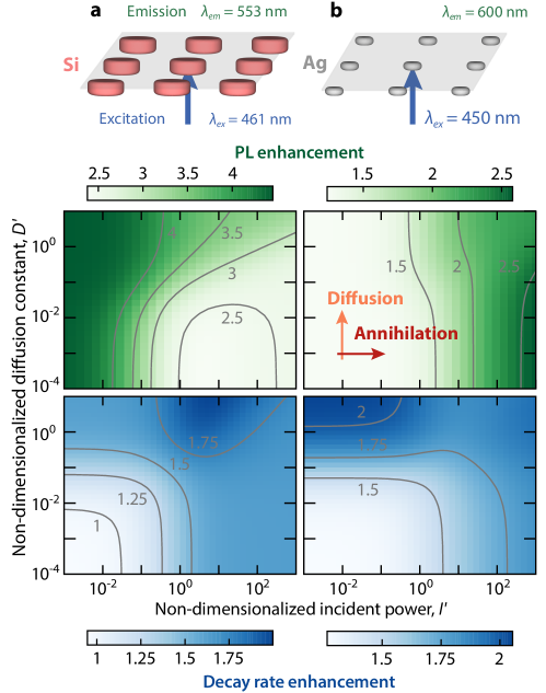
Next, we demonstrate that it is possible to improve performance even as annihilation becomes dominant. At low incident power, high- emitters benefit only from excitation enhancement whereas at high power, the effect of excitation diminishes and emission enhancement becomes dominant (Table 1). Therefore, nanophotonic structures with emission enhancement comparable to or higher than excitation enhancement offer improved photoluminescence enhancement with increasing power. This counter-intuitive behavior arises from the increasing benefit of emission enhancement as a strong non-radiative decay channel opens at high exciton densities. We exemplify such a case with an array of silver nanoparticles which has significantly higher emission enhancement compared to excitation enhancement (Supporting Figure S4). Indeed, as the incident power increases, emitters above the array of silver nanoparticles benefit from increasing photoluminescence enhancement. (Figure 6b). Although we have shown improved performance here for plasmonic nanoparticles, dielectric nanostructures with strong emission enhancements behave similarly (Supporting Figure S5). High- emitters with exciton-exciton annihilation are important for light-emitting devices, which suffer from efficiency loss at high powers. The ability to reduce the impact of annihilation on emission through the combination of nanophotonic design and diffusion is thus of practical interest.
2.4 Nanophotonic enhancement in relevant excitonic materials
Finally, we show that the non-dimensionalized limits of diffusion and annihilation become significant for light emission from realistic excitonic emitters. We tabulate reported excitonic parameters for representative materials and calculate their characteristic exciton density , incident power and the non-dimensionalized diffusion constant (Supporting Table S1). For transition metal dichalcogenide monolayers and two-dimensional perovskites, is of the order of unity. As a result, the excitons spread through the entire unit cell before they decay. Monolayer semiconductors with low quantum yield thus benefit from additional enhancement in nanostructures designed for diffusive excitons (Supporting Figure S6). Emitters with high quantum yield also suffer from strong annihilation . The incident power at which annihilation becomes dominant, , is very low (of the order of nW/m2 – W/m2), especially for transition metal dichalcogenides (Supporting Table S1). As a result, they benefit from additional enhancement in nanophotonic systems designed for materials with high annihilation (Supporting Figure S7).
Although we focused our analysis on excitons in thin films, the general principles also apply to other geometries. Nanowires support one-dimensional diffusion and can be placed along directions of high excitation and emission enhancements to obtain stronger photoluminescence (Supporting Figure S10). In the case of thick excitonic materials around nanophotonic structures, exciton diffusion will be three-dimensional, and the decay of the evanescent near field away from the nanostructure plane will also play a role. In addition to photonic enhancement, material interfaces can modify intrinsic decay, diffusion, and annihilation through doping, dielectric screening, or phonons 33, 39, 40, 41, 42, 43, 29. Our model can accommodate such effects through the use of locally varying excitonic parameters modified by the environment. It is also possible to prevent such environmental modification of excitonic parameters with a thin dielectric spacer. At high exciton densities in transition metal dichalcogenide monolayers, exciton-phonon effects modify diffusion, resulting in halo formation 44, 45, 46. Making the diffusion constant dependent on the exciton density 44 in the exciton dynamics equation can model such behavior. Some materials show superdiffusive behavior where the exciton density spreads faster than the prediction from linear diffusion. A rate equation model can describe such behavior by making the diffusion constant dependent on time or exciton density 47, 48. In materials such as organic semiconductors where there are multiple varieties of excitons, incorporating their interconversion into the rate equation can identify effects such as negative diffusion 49. Additional phenomena could further exploit diffusion to improve performance. Diffusion spreads the excitons away from the nanostructures, where Ohmic losses in the nanophotonic system are stronger. The reduction of absorption losses could therefore further contribute to total enhancement due to diffusion. Analogous to annihilation, saturation effects at higher excitation powers can suppress the enhancement 50 and could be similarly overcome through diffusion On the other hand, designing nanophotonic systems with extremely high emission enhancements can counteract the effect of diffusion by reducing the lifetime and thus the diffusion length (Supporting Figure S9). Last, applying strain on monolayer semiconductors can result in exciton funneling, the directional transport of excitons towards regions of high strain 51, 52, 53, 38, 54. Using nanostructures as sources of both strain and nanophotonic enhancement promises a new direction to control light-matter interaction.
3 Conclusion
We have combined exciton dynamics and nanophotonics to illustrate the range of scenarios beyond the conventional Purcell effect for photoluminescence enhancement in the presence of diffusion and annihilation. Although usually detrimental for light emission, careful nanophotonic design can turn diffusion into an advantage and partly mitigate the detrimental effect of exciton-exciton annihilation. We presented analytical expressions of enhancement for the limiting regimes of diffusion and annihilation to formulate the conditions for improved exciton photoluminescence. Removing the spatial overlap between excitation and emission enhancements can improve emission from diffusive excitons in nanostructured landscapes – for instance, by including a Stokes shift between excitation and emission wavelengths. Similar decoupling is possible through other strategies such as excitation and emission at different angles. It is also possible to alleviate the detrimental effects of exciton-exciton annihilation by tuning the relative strengths of excitation and emission enhancements and by capitalizing on diffusion to reduce the local exciton density. The approach could be extended to electrically generated excitons, which can create highly localized exciton distributions near nanoscale contacts. Additionally, solar cells could benefit from maximizing excitation enhancement near the nanostructures while redistributing the exciton density through diffusion to reduce the loss of excitons through emission and annihilation.
Our results demonstrate the importance of tailoring nanophotonic structures to specific exciton dynamics for maximal performance. As several excitonic materials consist of nano- or microcrystals exhibiting nanophotonic resonances, their photonic properties also have implications for understanding and quantifying exciton dynamics in nanomaterials. The operation principles and limiting regimes that we provide for diffusion and annihilation in nanophotonic landscapes can thus guide the design of efficient and high-power devices. Our findings apply to light-emitting diodes or lasers using relevant families of semiconductors in the form of nanoparticles, nanowires, thin films, or monolayers.
4 Methods
4.1 Electromagnetic simulations
We perform the electromagnetic simulations using the surface integral equation (SIE) method for periodic nanostructures 55, 56. We use the permittivities of silicon and silver from Green 57 and Johnson and Christy 58. We set a homogeneous relative permittivity for the background medium as the geometric mean of air and glass to approximate the effect of a substrate. We apply a realistic rounding radius of 20 nm to the sharp edges of the nanodisks.
We treat the emitters as electric dipole sources lying on a plane 5 nm above the nanodisks. To compute the excitation enhancement , we illuminate the system with a plane wave under normal incidence from above or below depending on optimal excitation conditions and evaluate the electric field on the plane above the nanostructure. The excitation enhancement for dipolar emitters orientationally averaged in three dimensions is , where is the electric field in the absence of the nanostructures.
The emission enhancement is the integral of the power radiated in all directions ), normalized to the same quantity in the absence of nanostructures. We compute the dipole radiation in a given direction using electromagnetic reciprocity 59 by evaluating the field intensity at the location of the emitter under illumination by a plane wave incident from the same direction 60, 61, 62. This method assumes no absorption losses in the nanodisks that might reduce antenna radiation efficiency. The emission enhancement of a dipole depends on its orientation. We compute the average emission enhancements for emitters along all possible orientations in three dimensions, integrating total photoluminescence in all directions.
For emitters such as transition metal dichalcogenides where the dipoles are oriented in the plane, excitation enhancement requires using the in-plane projection of the electric field. Additionally, orientational averaging should then be performed in two dimensions. With these modifications, our treatment applies to two-dimensional excitonic materials as well and does not change the results qualitatively (Supporting Figure S8).
4.2 Numerical solution of exciton dynamics
To solve the non-dimensionalized exciton dynamics equation (2.1) numerically, we discretize the exciton density into a grid with non-dimensionalized coordinates: where for . We choose the value of in each simulation to obtain nm spatial resolution. As a result of periodicity, the exciton densities are equal at opposite edges of the unit cell (indices and ). In the limiting case of low incident power, the quadratic annihilation term vanishes, and we obtain a linear differential equation in . Under continuous-wave illumination, in the steady state, we have where we have dropped the explicit spatial dependence. Taking the spatial Fourier transform,
| (1) |
where the quantities with a tilde (such as ) are Fourier transforms of the real-space quantities, is the circular convolution matrix for , and the matrix is the squared momentum in the Fourier transform of the discrete Laplace operator, with elements . Inverting the matrix on the left-hand side of Equation (1) gives the steady-state exciton density. Its eigenvalues describe the time evolution under pulsed illumination, providing the total decay rate enhancement.
In the presence of annihilation, we can no longer use linear methods. Hence we let the system evolve explicitly according to Equation (2.1) using the forward Euler method until . Under continuous-wave illumination, the system reaches a steady state by this time. We model pulsed excitation using an ultrashort impulse so that the exciton density instantaneously becomes . We ensure that the high initial decay rates do not result in numerical errors by using an adaptive time step that limits the maximum relative change in exciton density at a location within a time step to one percent. The total photoluminescence from the unit cell is then
| (2) |
We can also calculate the decay time as the mean lifetime of emission from the temporal decay of photoluminescence:
| (3) |
The total decay rate enhancement is the ratio of the decay time without the nanostructure to the average decay time in the presence of the nanostructure.
Supporting Information
Supporting Information is available from the Wiley Online Library or from the author.
Acknowledgements
We thank Rasmus H. Godiksen for illuminating discussions. This work was financially supported by the Netherlands Organization for Scientific Research (NWO) through Gravitation grant “Research Centre for Integrated Nanophotonics” (024.002.033), START-UP grant (740.018.009), and Innovational Research Incentives Scheme (VICI Grant nr. 680-47-628). S. Wang was supported by Priority Academic Program Development (PAPD) of Jiangsu Higher Education Institutions. Simulations in this work were carried out on the Dutch national e-infrastructure with the support of SURF Cooperative.
Conflict of interest
The authors declare that they have no conflict of interest.
References
- Bidault et al. 2019 Bidault, S.; Mivelle, M.; Bonod, N. Dielectric nanoantennas to manipulate solid-state light emission. J. Appl. Phys. 2019, 126, 094104
- Tiguntseva et al. 2018 Tiguntseva, E. Y.; Zograf, G. P.; Komissarenko, F. E.; Zuev, D. A.; Zakhidov, A. A.; Makarov, S. V.; Kivshar, Y. S. Light-Emitting Halide Perovskite Nanoantennas. Nano Lett. 2018, 18, 1185–1190
- Rutckaia et al. 2017 Rutckaia, V.; Heyroth, F.; Novikov, A.; Shaleev, M.; Petrov, M.; Schilling, J. Quantum Dot Emission Driven by Mie Resonances in Silicon Nanostructures. Nano Lett. 2017, 17, 6886–6892
- Bucher et al. 2019 Bucher, T.; Vaskin, A.; Mupparapu, R.; Löchner, F. J. F.; George, A.; Chong, K. E.; Fasold, S.; Neumann, C.; Choi, D.-Y.; Eilenberger, F.; Setzpfandt, F.; Kivshar, Y. S.; Pertsch, T.; Turchanin, A.; Staude, I. Tailoring Photoluminescence from MoS2 Monolayers by Mie-Resonant Metasurfaces. ACS Photonics 2019, 6, 1002–1009
- Raziman et al. 2019 Raziman, T. V.; Godiksen, R. H.; Müller, M. A.; Curto, A. G. Conditions for Enhancing Chiral Nanophotonics near Achiral Nanoparticles. ACS Photonics 2019, 6, 2583–2589
- Murai et al. 2020 Murai, S.; Castellanos, G. W.; Raziman, T. V.; Curto, A. G.; Gómez Rivas, J. Enhanced Light Emission by Magnetic and Electric Resonances in Dielectric Metasurfaces. Adv. Opt. Mater. 2020, n/a, 1902024
- Cihan et al. 2018 Cihan, A. F.; Curto, A. G.; Raza, S.; Kik, P. G.; Brongersma, M. L. Silicon Mie resonators for highly directional light emission from monolayer MoS2. Nat. Photon. 2018, 12, 284–290
- Farahani et al. 2005 Farahani, J. N.; Pohl, D. W.; Eisler, H.-J.; Hecht, B. Single Quantum Dot Coupled to a Scanning Optical Antenna: A Tunable Superemitter. Phys. Rev. Lett. 2005, 95, 017402
- Anger et al. 2006 Anger, P.; Bharadwaj, P.; Novotny, L. Enhancement and Quenching of Single-Molecule Fluorescence. Phys. Rev. Lett. 2006, 96, 113002
- Kühn et al. 2006 Kühn, S.; Håkanson, U.; Rogobete, L.; Sandoghdar, V. Enhancement of Single-Molecule Fluorescence Using a Gold Nanoparticle as an Optical Nanoantenna. Phys. Rev. Lett. 2006, 97, 017402
- Vecchi et al. 2009 Vecchi, G.; Giannini, V.; Gómez Rivas, J. Shaping the Fluorescent Emission by Lattice Resonances in Plasmonic Crystals of Nanoantennas. Phys. Rev. Lett. 2009, 102, 146807
- Curto et al. 2010 Curto, A. G.; Volpe, G.; Taminiau, T. H.; Kreuzer, M. P.; Quidant, R.; van Hulst, N. F. Unidirectional Emission of a Quantum Dot Coupled to a Nanoantenna. Science 2010, 329, 930–933
- Huang et al. 2012 Huang, K. C. Y.; Seo, M.-K.; Huo, Y.; Sarmiento, T.; Harris, J. S.; Brongersma, M. L. Antenna electrodes for controlling electroluminescence. Nat. Commun. 2012, 3, 1–6
- Mohammadi et al. 2008 Mohammadi, A.; Sandoghdar, V.; Agio, M. Gold nanorods and nanospheroids for enhancing spontaneous emission. New J. Phys. 2008, 10, 105015
- Novotny and Hecht 2012 Novotny, L.; Hecht, B. Principles of Nano-Optics, 2nd ed.; Cambridge University Press, 2012
- Stranks et al. 2013 Stranks, S. D.; Eperon, G. E.; Grancini, G.; Menelaou, C.; Alcocer, M. J. P.; Leijtens, T.; Herz, L. M.; Petrozza, A.; Snaith, H. J. Electron-Hole Diffusion Lengths Exceeding 1 Micrometer in an Organometal Trihalide Perovskite Absorber. Science 2013, 342, 341–344
- Yao et al. 2019 Yao, E.-P.; Bohn, B. J.; Tong, Y.; Huang, H.; Polavarapu, L.; Feldmann, J. Exciton Diffusion Lengths and Dissociation Rates in CsPbBr3 Nanocrystal–Fullerene Composites: Layer-by-Layer versus Blend Structures. Adv. Opt. Mater. 2019, 7, 1801776
- Deng et al. 2020 Deng, S.; Shi, E.; Yuan, L.; Jin, L.; Dou, L.; Huang, L. Long-range exciton transport and slow annihilation in two-dimensional hybrid perovskites. Nat. Commun. 2020, 11, 1–8
- Kumar et al. 2014 Kumar, N.; Cui, Q.; Ceballos, F.; He, D.; Wang, Y.; Zhao, H. Exciton diffusion in monolayer and bulk MoSe2. Nanoscale 2014, 6, 4915–4919
- Yuan et al. 2017 Yuan, L.; Wang, T.; Zhu, T.; Zhou, M.; Huang, L. Exciton Dynamics, Transport, and Annihilation in Atomically Thin Two-Dimensional Semiconductors. J. Phys. Chem. Lett. 2017, 8, 3371–3379
- Akselrod et al. 2014 Akselrod, G. M.; Prins, F.; Poulikakos, L. V.; Lee, E. M. Y.; Weidman, M. C.; Mork, A. J.; Willard, A. P.; Bulović, V.; Tisdale, W. A. Subdiffusive Exciton Transport in Quantum Dot Solids. Nano Lett. 2014, 14, 3556–3562
- Lee and Tisdale 2015 Lee, E. M. Y.; Tisdale, W. A. Determination of Exciton Diffusion Length by Transient Photoluminescence Quenching and Its Application to Quantum Dot Films. J. Phys. Chem. C 2015, 119, 9005–9015
- Mikhnenko et al. 2015 Mikhnenko, O. V.; Blom, P. W. M.; Nguyen, T.-Q. Exciton diffusion in organic semiconductors. Energy Environ. Sci. 2015, 8, 1867–1888
- Cognet et al. 2007 Cognet, L.; Tsyboulski, D. A.; Rocha, J.-D. R.; Doyle, C. D.; Tour, J. M.; Weisman, R. B. Stepwise Quenching of Exciton Fluorescence in Carbon Nanotubes by Single-Molecule Reactions. Science 2007, 316, 1465–1468
- Amori et al. 2018 Amori, A. R.; Hou, Z.; Krauss, T. D. Excitons in Single-Walled Carbon Nanotubes and Their Dynamics. Annu. Rev. Phys. Chem. 2018, 69, 81–99
- Hertel et al. 2010 Hertel, T.; Himmelein, S.; Ackermann, T.; Stich, D.; Crochet, J. Diffusion Limited Photoluminescence Quantum Yields in 1-D Semiconductors: Single-Wall Carbon Nanotubes. ACS Nano 2010, 4, 7161–7168
- Li et al. 2018 Li, W.; Yadavalli, S. K.; Lizarazo-Ferro, D.; Chen, M.; Zhou, Y.; Padture, N. P.; Zia, R. Subgrain Special Boundaries in Halide Perovskite Thin Films Restrict Carrier Diffusion. ACS Energy Lett. 2018, 3, 2669–2670
- Snaider et al. 2018 Snaider, J. M.; Guo, Z.; Wang, T.; Yang, M.; Yuan, L.; Zhu, K.; Huang, L. Ultrafast Imaging of Carrier Transport across Grain Boundaries in Hybrid Perovskite Thin Films. ACS Energy Lett. 2018, 3, 1402–1408
- Goodman et al. 2020 Goodman, A. J.; Lien, D.-H.; Ahn, G. H.; Spiegel, L. L.; Amani, M.; Willard, A. P.; Javey, A.; Tisdale, W. A. Substrate-Dependent Exciton Diffusion and Annihilation in Chemically Treated MoS2 and WS2. J. Phys. Chem. C 2020,
- Yuan and Huang 2015 Yuan, L.; Huang, L. Exciton dynamics and annihilation in WS2 2D semiconductors. Nanoscale 2015, 7, 7402–7408
- Sun et al. 2014 Sun, D.; Rao, Y.; Reider, G. A.; Chen, G.; You, Y.; Brézin, L.; Harutyunyan, A. R.; Heinz, T. F. Observation of Rapid Exciton–Exciton Annihilation in Monolayer Molybdenum Disulfide. Nano Lett. 2014, 14, 5625–5629
- Mouri et al. 2014 Mouri, S.; Miyauchi, Y.; Toh, M.; Zhao, W.; Eda, G.; Matsuda, K. Nonlinear photoluminescence in atomically thin layered WSe2 arising from diffusion-assisted exciton-exciton annihilation. Phys. Rev. B 2014, 90, 155449
- Yu et al. 2016 Yu, Y.; Yu, Y.; Xu, C.; Barrette, A.; Gundogdu, K.; Cao, L. Fundamental limits of exciton-exciton annihilation for light emission in transition metal dichalcogenide monolayers. Phys. Rev. B 2016, 93, 201111
- Raziman and Martin 2016 Raziman, T. V.; Martin, O. J. F. Orientation Dependence of Plasmonically Enhanced Spontaneous Emission. J. Phys. Chem. C 2016, 120, 21037–21046
- Sun et al. 2009 Sun, G.; Khurgin, J. B.; Soref, R. A. Practical enhancement of photoluminescence by metal nanoparticles. Appl. Phys. Lett. 2009, 94, 101103
- Kinkhabwala et al. 2009 Kinkhabwala, A.; Yu, Z.; Fan, S.; Avlasevich, Y.; Müllen, K.; Moerner, W. E. Large single-molecule fluorescence enhancements produced by a bowtie nanoantenna. Nat. Photonics 2009, 3, 654–657
- Mey et al. 2019 Mey, O.; Wall, F.; Schneider, L. M.; Günder, D.; Walla, F.; Soltani, A.; Roskos, H.; Yao, N.; Qing, P.; Fang, W.; Rahimi-Iman, A. Enhancement of the Monolayer Tungsten Disulfide Exciton Photoluminescence with a Two-Dimensional Material/Air/Gallium Phosphide In-Plane Microcavity. ACS Nano 2019, 13, 5259–5267
- Sortino et al. 2019 Sortino, L.; Zotev, P. G.; Mignuzzi, S.; Cambiasso, J.; Schmidt, D.; Genco, A.; Aßmann, M.; Bayer, M.; Maier, S. A.; Sapienza, R.; Tartakovskii, A. I. Enhanced light-matter interaction in an atomically thin semiconductor coupled with dielectric nano-antennas. Nat. Commun. 2019, 10, 5119
- Hoshi et al. 2017 Hoshi, Y.; Kuroda, T.; Okada, M.; Moriya, R.; Masubuchi, S.; Watanabe, K.; Taniguchi, T.; Kitaura, R.; Machida, T. Suppression of exciton-exciton annihilation in tungsten disulfide monolayers encapsulated by hexagonal boron nitrides. Phys. Rev. B 2017, 95, 241403
- Schneider et al. 2018 Schneider, L. M.; Lippert, S.; Kuhnert, J.; Ajayi, O.; Renaud, D.; Firoozabadi, S.; Ngo, Q.; Guo, R.; Kim, Y. D.; Heimbrodt, W.; Hone, J. C.; Rahimi-Iman, A. The influence of the environment on monolayer tungsten diselenide photoluminescence. Nano-Structures & Nano-Objects 2018, 15, 84–97
- Fu et al. 2019 Fu, Y.; He, D.; He, J.; Bian, A.; Zhang, L.; Liu, S.; Wang, Y.; Zhao, H. Effect of Dielectric Environment on Excitonic Dynamics in Monolayer WS2. Adv. Mater. Interf. 2019, 6, 1901307
- Rhodes et al. 2019 Rhodes, D.; Chae, S. H.; Ribeiro-Palau, R.; Hone, J. Disorder in van der Waals heterostructures of 2D materials. Nat. Mater. 2019, 18, 541–549
- Godiksen et al. 2020 Godiksen, R. H.; Wang, S.; Raziman, T. V.; Guimaraes, M. H. D.; Rivas, J. G.; Curto, A. G. Correlated Exciton Fluctuations in a Two-Dimensional Semiconductor on a Metal. Nano Lett. 2020, 20, 4829–4836
- Kulig et al. 2018 Kulig, M.; Zipfel, J.; Nagler, P.; Blanter, S.; Schüller, C.; Korn, T.; Paradiso, N.; Glazov, M. M.; Chernikov, A. Exciton Diffusion and Halo Effects in Monolayer Semiconductors. Phys. Rev. Lett. 2018, 120, 207401
- Glazov 2019 Glazov, M. M. Phonon wind and drag of excitons in monolayer semiconductors. Phys. Rev. B 2019, 100, 045426
- Perea-Causín et al. 2019 Perea-Causín, R.; Brem, S.; Rosati, R.; Jago, R.; Kulig, M.; Ziegler, J. D.; Zipfel, J.; Chernikov, A.; Malic, E. Exciton Propagation and Halo Formation in Two-Dimensional Materials. Nano Lett. 2019, 19, 7317–7323
- Najafi et al. 2017 Najafi, E.; Ivanov, V.; Zewail, A.; Bernardi, M. Super-diffusion of excited carriers in semiconductors. Nat. Commun. 2017, 8
- Flekkøy et al. 2021 Flekkøy, E. G.; Hansen, A.; Baldelli, B. Hyperballistic Superdiffusion and Explosive Solutions to the Non-Linear Diffusion Equation. Frontiers in Physics 2021, 9
- Berghuis et al. 2021 Berghuis, A. M.; Raziman, T. V.; Halpin, A.; Wang, S.; Curto, A. G.; Rivas, J. G. Effective Negative Diffusion of Singlet Excitons in Organic Semiconductors. J. Phys. Chem. Lett. 2021, 12, 1360–1366
- Kern et al. 2012 Kern, A. M.; Meixner, A. J.; Martin, O. J. F. Molecule-Dependent Plasmonic Enhancement of Fluorescence and Raman Scattering near Realistic Nanostructures. ACS Nano 2012, 6, 9828–9836
- Castellanos-Gomez et al. 2013 Castellanos-Gomez, A.; Roldán, R.; Cappelluti, E.; Buscema, M.; Guinea, F.; van der Zant, H. S. J.; Steele, G. A. Local Strain Engineering in Atomically Thin MoS2. Nano Lett. 2013, 13, 5361–5366
- Liu and Guo 2019 Liu, X.; Guo, W. Shear strain tunable exciton dynamics in two-dimensional semiconductors. Phys. Rev. B 2019, 99, 035401
- Moon et al. 2019 Moon, H.; Grosso, G.; Chakraborty, C.; Peng, C.; Taniguchi, T.; Watanabe, K.; Englund, D. Dynamic exciton funneling by local strain control in a monolayer semiconductor. arXiv:1906.10077 [cond-mat] 2019,
- Sortino et al. 2020 Sortino, L.; Brooks, M.; Zotev, P. G.; Genco, A.; Cambiasso, J.; Mignuzzi, S.; Maier, S. A.; Burkard, G.; Sapienza, R.; Tartakovskii, A. I. Dielectric Nanoantennas for Strain Engineering in Atomically Thin Two-Dimensional Semiconductors. ACS Photonics 2020, 7, 2413–2422
- Gallinet et al. 2010 Gallinet, B.; Kern, A. M.; Martin, O. J. F. Accurate and versatile modeling of electromagnetic scattering on periodic nanostructures with a surface integral approach. J. Opt. Soc. Am. A 2010, 27, 2261–2271
- Raziman et al. 2015 Raziman, T. V.; Somerville, W. R. C.; Martin, O. J. F.; Le Ru, E. C. Accuracy of surface integral equation matrix elements in plasmonic calculations. J. Opt. Soc. Am. B 2015, 32, 485–492
- Green 2008 Green, M. A. Self-consistent optical parameters of intrinsic silicon at 300K including temperature coefficients. Sol. Energy Mater. Sol. Cells 2008, 92, 1305–1310
- Johnson and Christy 1972 Johnson, P. B.; Christy, R. W. Optical Constants of the Noble Metals. Phys. Rev. B 1972, 6, 4370–4379
- Chew 1990 Chew, W. C. Waves and Fields in Inhomogeneous Media; Van Nostrand Reinhold, 1990
- Anttu 2016 Anttu, N. Modifying the emission of light from a semiconductor nanowire array. J. Appl. Phys. 2016, 120, 043108
- Kivisaari et al. 2018 Kivisaari, P.; Chen, Y.; Anttu, N. Emission enhancement, light extraction and carrier dynamics in InGaAs/GaAs nanowire arrays. Nano Futures 2018, 2, 015001
- Vaskin et al. 2018 Vaskin, A.; Bohn, J.; Chong, K. E.; Bucher, T.; Zilk, M.; Choi, D.-Y.; Neshev, D. N.; Kivshar, Y. S.; Pertsch, T.; Staude, I. Directional and Spectral Shaping of Light Emission with Mie-Resonant Silicon Nanoantenna Arrays. ACS Photonics 2018, 5, 1359–1364