Apparent Differences between Single Layer Molybdenum Disulfide Fabricated via Chemical Vapor Deposition and Exfoliation
Abstract
Innovative applications based on two-dimensional solids require cost-effective fabrication processes resulting in large areas of high quality materials. Chemical vapour deposition is among the most promising methods to fulfill these requirements. However, for 2D materials prepared in this way it is generally assumed that they are of inferior quality in comparison to the exfoliated 2D materials commonly used in basic research. In this work we challenge this assumption and aim to quantify the differences in quality for the prototypical transition metal dichalcogenide MoS2. To this end single layers of MoS2 prepared by different techniques (exfoliation, grown by different chemical vapor deposition methods, transfer techniques, and as vertical heterostructure with graphene) are studied by Raman and photoluminescence spectroscopy, complemented by atomic force microscopy. We demonstrate that as-prepared MoS2, directly grown on SiO2, differs from exfoliated MoS2 in terms of higher photoluminescence, lower electron concentration, and increased strain. As soon as a water film is intercalated (e.g., by transfer) underneath the grown MoS2, in particular the (opto-)electronic properties become practically identical to those of exfoliated MoS2. A comparison of the two most common precursors shows that the growth with MoO3 causes greater strain and/or defect density deviations than growth with ammonium heptamolybdate. As part of a heterostructure directly grown MoS2 interacts much stronger with the substrate, and in this case an intercalated water film does not lead to the complete decoupling, which is typical for exfoliation or transfer. Our work shows that the supposedly poorer quality of grown 2D transition metal dichalcogenides is indeed a misconception.
keywords:
Chemical Vapour Deposition, MoS2, 2D Materials, van der Waals Heterostructures, Raman Spectroscopypresent affiliation: Technical Chemistry III – Faculty of Chemistry, University of Duisburg-Essen, Carl-Benz-Straße 199, 47057 Duisburg, Germany \altaffiliationSchool of Material Science and Engineering, University of New South Wales, AUS-2052 Sydney, Australia \abbreviations2D, MoS2, MoO3, AHM, TMDC, CVD, vdW, PL, AFM
1 Introduction
Two-dimensional (2D) materials are in general thin, flexible, and transparent and it is expected that the semiconducting ones among them will soon play an important role in the development of flexible (opto)electronics. In particular, the possibility to stack different 2D materials to design artificial solids with tailored and otherwise inaccessible (opto)electronic properties, has opened the door for a technological breakthrough. However, one of the biggest obstacles that must be overcome before any dreams of real-world application may come true is the manufacturing process: While researchers rely heavily on isolating techniques yielding individual crystallites of 2D materials, industrial implementation requires growth techniques which are scalable, cost-effective, and reliable.
Several hundred 2D materials could be realized so far, but the transition metal dichalcogenides (TMDCs) are the most intensively studied. This is certainly due to their physical properties, such as a large band gap in the visible range, but also to the fact that they are relatively easy to produce. Like graphene, TMDC monolayers can be isolated, e.g., by mechanical exfoliation 1, 2 and can be grown, e.g., via chemical vapour deposition (CVD) 3, 4, 5. Like in the case of graphene, most basic research is still done with exfoliated flakes as it is commonly believed that their quality exceeds that of CVD grown flakes. However, the term quality usually refers to defect densities, and it has already been shown that 2D materials grown by CVD can exhibit defect densities which are comparable to those of exfoliated material 6. Thus, for graphene, being metallic, the common belief could indeed be true, as any crystalline defects are detrimental for its outstanding transport properties. For the optoelectronic properties of a semiconducting 2D material, however, appropriate quality criteria might be quite different. For example, the comparison between CVD grown MoS2 with exfoliated MoS2, both on sapphire 4, or in this study on SiO2 (see Fig. 1 below), shows a much higher photoluminescence (PL) intensity in the case of CVD growth. Not as obvious as the intensity of a PL signal, but equally important, are the changes of the Raman mode positions for MoS2 fabricated from CVD and exfoliation, which can be directly attributed to physical properties such as strain and doping 7, 8, 9, 10, 11, 12, 13, 14, 15.
A pertinent problem in this context is that any comparison between 2D materials from CVD and exfoliated 2D materials requires that the materials be measured under the same or at least similar environmental conditions. Otherwise, if distinct differences are revealed, they can either be attributed to the material’s quality, e.g., preparation-specific inhomogeneities, but they could also originate from preparation conditions or the chosen substrate 16, 17, 18, as 2D materials are extremely sensitive to their immediate surroundings. For van der Waals (vdW) heterostructures this becomes even more critical as a number of interfaces are involved which may involve any combination of exfoliated and CVD grown materials. The lack of spectroscopic data taken on differently prepared samples under the strict condition of similar environmental conditions renders it currently almost impossible to decide, how much of what has been derived from experiments on exfoliated materials, or whether any of the reported proof-of-principle concepts may be transferred to CVD grown material at all.
In this paper we fill this crucial gap and clarify the origin of apparent spectroscopic (PL, Raman) differences found for MoS2 either grown by CVD or isolated by exfoliation. For our comprehensive study we use exfoliated MoS2 as a reference system, grow samples via CVD using two different precursors (molybdenum trioxid (MoO3) and ammonium heptamolybdate (AHM)) and apply transfer techniques to obtain similar environmental conditions for MoS2 fabricated by exfoliation and by CVD, respectively. Our experimental data shows that as prepared, MoS2 directly grown on SiO2 differs from exfoliated MoS2 in terms of higher photoluminescence, lower electron concentration, and increased strain, seemingly supporting the widely shared belief of supposedly superior quality of exfoliated material. However, adding intercalated water turns the picture upside-down: We provide clear evidence by Raman spectroscopy in conjunction with PL spectroscopy and atomic force microscopy (AFM) that the intrinsic properties of exfoliated and CVD grown are, in fact, almost identical. Any spectroscopically observed differences can unambiguously be attributed to the presence or absence of an intercalated water film, respectively. Our findings are further supported with experiments performed on aged samples and extended to a prototypical MoS2-graphene heterostructure. From our results we conclude that MoS2 grown with the right precursor (AHM) may serve as a more-than-adequate substitute for exfoliated material.
2 Results and Discussion
Overview and Key Question
We start by introducing the sample systems studied in this paper. Figure 1 (a) presents the seven different single layer MoS2 systems under investigation: exfoliated MoS2 on SiO2 (blue square), MoS2 grown by CVD with AHM precursor on SiO2 (light blue triangle) and transferred onto SiO2 (light blue square), MoS2 grown by CVD with MoO3 powder source on SiO2 (green triangle) and transferred onto SiO2 (green square), MoS2 directly grown on transferred CVD graphene (orange triangle), and CVD grown MoS2 transferred onto transferred CVD graphene (orange square). The images from the optical microscope are all identical in size – the scalebars correspond to 20 µm. This substantiates one of the well-known advantages of CVD over exfoliation as a fabrication method for 2D materials: a significantly larger flake size.
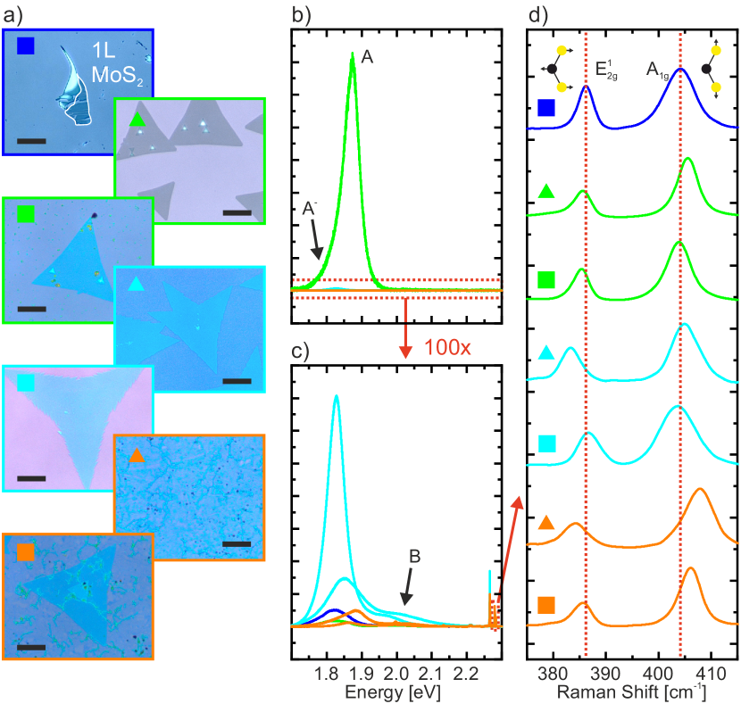
For a first comparison of our sample systems we performed PL and Raman spectroscopy, see Fig. 1 (b)-(d). The obtained PL spectra in Fig. 1 (b) and (c) show the characteristic exciton and trion peaks of MoS2 19, 20, 21. The most prominent peak between 1.8 and 1.9 eV corresponds to the A exciton, the peak around 2.0 eV to the B exciton. The A- trion peak can been found as a shoulder of the A exciton peak around 1.8 eV. Apparently, the spectroscopic signature of single layers of MoS2 prepared differently shows a large variation. Note that, while the variation between sample systems is large, the spectra shown in Fig. 1 are nevertheless typical and thus representative for any given sample system.
Because our analysis is based on a comparison of differently prepared samples we present in Fig. 2 schematic illustrations of our sample systems together with a compilation of our data before discussing the individual samples further below. In Fig. 2 (b) and (c) the PL intensities (total area of all exciton and trion peaks) and the intensity ratio B/(A+A-) for the representative PL spectra from Fig. 1 are shown, respectively. All intensities are normalized to the applied laser power and the integration time, thus to the number of incident photons. The ratio B/(A+A-) refers to the (area) intensity ratio of the peaks of the A exciton, the B exciton, and the A- trion, respectively. Figure 2 (d) shows the position of the E (around 385 cm-1) and the A1g (around 405 cm-1) Raman mode as an average of the acquired Raman spectra. In addition to spectroscopy we performed supportive AFM measurements to determine the thickness of the MoS2 layers, see SI for a selection of AFM images and line scans and Fig. 2 (e) for the resulting thicknesses. Note that the intercalated water layers depicted in Fig. 2 (a) were not added on purpose to our sample system. They are nevertheless present and turn out to be the key factor for some of the properties as will be shown further below.
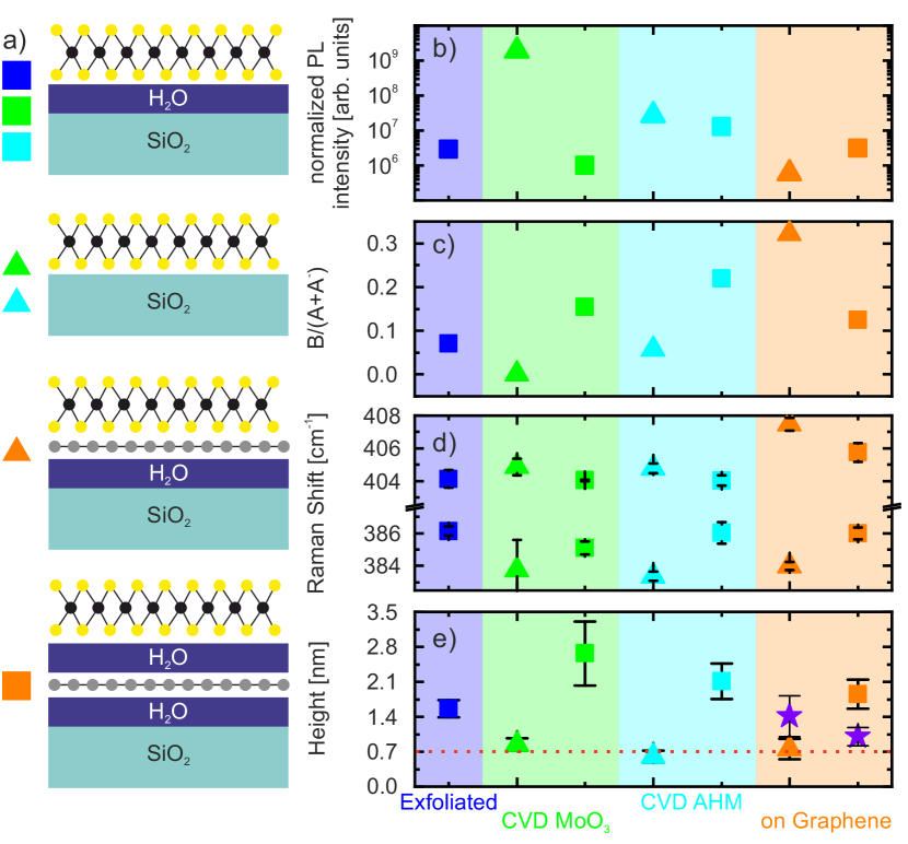
In order to reveal the origin of the systematic variations we will now discuss the individual features in detail by discussing PL, Raman, and AFM results for each sample system. We start by comparing the two most well known single layer MoS2 systems: exfoliated (blue squares) and directly grown CVD MoS2 (green and light blue triangles), both on SiO2. From Fig. 2 (b) it can be seen that the total PL intensity of CVD grown MoS2 is up to three orders of magnitude larger than for the exfoliated counterpart. Therefore, from the PL point of view CVD MoS2 is clearly superior to exfoliated MoS2. The higher intensities make CVD MoS2 the material of choice for optoelectronic applications.
From the PL spectra more information about the MoS2 can be extracted. Mak et al. reported a decreasing A/A- ratio with increasing charge carrier concentration in single layer MoS2 21. Actually, the A exciton intensity is almost exclusively influenced by the charge carrier concentration. Although not discussed by Mak et al., but shown by their data, the B exciton as well as the A- trion intensity remains relatively constant with changing charge carrier concentration. As it can be difficult to seperate the A and the A- peak correctly – they are only a few 10 meV separated from each other – we use the B/(A+A-) ratio instead. From this, it can be qualitatively concluded that a high B/(A+A-) ratio means that the system is n-doped. For our comparison of CVD grown MoS2 (green and light blue triangles) with exfoliated MoS2 (blue square) this means that the latter is more n-doped by charge transfer from the substrate, see Fig. 2 (c). Unfortunately, the exciton peak ratio is not linearly dependent on the carrier concentration and the peaks – both, shifts and intensity ratio change – can be affected due to several other reasons such as defects 22, 23, strain 9, 10, 12, 24, 25, 14, incident laser power 22, 26, 27, 25, and dielectric screening 28, 25. Thus, the PL spectra are not suitable for a quantitative analysis, but will be used supportively in the following.
Next, we will show that the commonly used rule for single layer characterization by Raman spectroscopy has to be adapted for CVD material. The typical approach to interpret Raman spectra of MoS2 is to determine the difference between the position of the E and the A1g mode. The result gives an information about the number of layers: for exfoliated MoS2 a difference of 19 cm-1 corresponds to single layer, while a difference of 22 cm-1 is already attributed to a bilayer 29. Here, we find a difference of 18.0 0.75 cm-1 for exfoliated MoS2 (blue square), 21.1 1.55 cm-1 (green triangle), and 21.4 0.46 cm-1 (light blue triangle) for the MoS2 grown by the two different CVD methods, see Fig. 2 (d). The latter wave numbers are already quite close to the number for a bilayer in the case of exfoliated samples. However, the high PL intensity is a clear indication of the single layer nature of the grown material 20, 19, 30. This is further corroborated by the AFM data from Fig. 2 (e). It shows that the determined thickness of the directly grown MoS2 flakes (triangles) corresponds well with the expected thickness of one layer of MoS2 ( 0.7 nm). This is clear evidence, that the CVD MoS2 is indeed single layer. Exfoliated MoS2 flakes (blue square) are frequently found to be much thicker, but are identified as single layer from the Raman data. The reason for the increased thickness is most likely due to intercalated water between substrate and 2D material, which is often reported for exfoliated 2D materials 2, 31, 32, 33, 34, 35, 36. In contrast, during the CVD process the presence of a water film appears to be highly unlikely because temperatures up to 800 °C are present. As a result, the grown 2D material is in direct contact with the substrate and its true height might be accessed via AFM. The reason for the unusually large difference between the two Raman peaks in CVD grown MoS2 is thus not due to the presence of bilayer. Rather, the Raman mode positions are also affected by strain 7, 8, 9, 10, 11, 12, 13, 14 and the charge carrier concentration 15, 13. The shift of the E mode to higher and of the A1g mode to lower values, respectively, indicate qualitatively that the CVD material is exposed to higher strain and exhibits a lower charge carrier concentration. This will be discussed in more detail below.
So far we have seen that exfoliated and CVD grown MoS2 obviously differ in PL intensity, but also in doping and strain. This leads us to one of the key question of this paper. It is usually assumed that 2D materials grown by CVD directly as single layer have a lower structural quality than exfoliated materials, which are claimed to have a remarkably high quality 1, 2. The defect density and the grain size will of course affect the material’s properties but is this, and therefore the production method, really the reason for the observed differences in the properties of CVD grown MoS2 and exfoliated MoS2?
In order to answer this question we prepare sample systems from CVD grown MoS2 which can be directly compared to exfoliated MoS2. To this end CVD MoS2 flakes were transferred from their original growth substrate SiO2 onto a second, clean SiO2 substrate (green and light blue squares). The analysis of this system shows a decreased PL intensity, an increased B/(A+A-) ratio, a decreased Raman mode difference, and an increased flake thickness, see Fig. 2 (b)-(e). This means, that after the transfer of the CVD grown flake, the properties of the material appear now very similar, even almost identical, to those of exfoliated MoS2 (for this reason this type of samples is represented by a square in all diagrams, just like exfoliated MoS2). This finding is even more intriguing as one would have expected the transfer to rather degrade the overall quality of the material. Based on our results, we can at this point thus formulate two hypotheses: (i) the fabrication method itself has only a very minor influence on the intrinsic properties of single layer MoS2, and (ii) the dominant factor for the actual properties of 2D MoS2 is the presence or absence of an intercalated water film - which is a purely external effect.
Quantification by Transformation Matrix
Next, we will quantify the physical properties to validate our hypotheses. To this end, we present the Raman mode positions (from Fig. 2) for the differently prepared MoS2 systems in a different way: In Fig. 3 (a) the E mode position is plotted vs. the A1g mode position. This diagram makes it easier to identify groups of sample systems with similar behaviour. For the analysis we construct a matrix based on literature data taking into account the mode dependency on strain 7, 8, 9, 10, 11, 12, 13, 14 and doping 15, 13 allowing us to conduct an axis transformation as given by equation 1. All publications that have studied the evolution of Raman mode positions as a function of strain report that strain causes a shift of the E, while the A1g mode position is almost exclusively influenced by doping. Biaxial 11, 12, 13 and uniaxial strain 7, 8, 9, 10, 13, 14, however, differ with respect to the exact number of wave number shift per percentage of strain. Although MoS2 typically deforms in uniaxially strained wrinkels (orders of magnitude larger than the substrate roughness) 10, 37, 38, 39, 40, we assume that on the nanoscale the deformation of a MoS2 layer on a given substrate is a mixture of strained, unstrained, uniaxially and biaxially strained regions averaged by the µm2 laser spot. For the construction of the matrix we use thus the publication of Rice et al. 7 and Chakraborty et al. 15, who have quantified the strain- and doping-dependent Raman shift experimentally and by calculations. Note that Rice et al. only report uniaxial strain, which may cause some deviation in the absolute value.
| (1) |
This matrix can now be used to transform our E vs. A1g plot (or mode positions of a single spectrum with respect to a given reference spectrum) into a strain vs. n-doping plot, see Fig. 3 (b). Because mode position changes are considered with regard to a reference system, only relative strain and doping are shown. The ideal reference system would be a single layer MoS2 system with no strain and the intrinsic doping level. Unfortunately, especially the latter has not been achieved yet. For our discussion here we use exfoliated MoS2 as a reference (i.e. zero point for the axes in Fig. 3 (b)), a choice which can be justified by the following reasons: Exfoliation of single layer MoS2 is based on the detachment of the last layer from a bulk crystal. Even if the scotch tape would induce any strain in bulk MoS2, the multi layered nature of MoS2 in combination with the weak van der Waals forces in between layers ensure that any strain built into the last layer is released upon exfoliation.
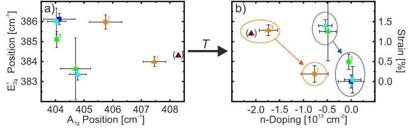
From the resulting diagram (Fig. 3 (b)) the strain and the n-doping can now be quantified with respect to exfoliated MoS2. As stated in our hypothesis and shown qualitatively before, transferred CVD grown MoS2 (green and light blue square) has very similar properties to exfoliated MoS2 (blue square) indeed. However, directly grown MoS2 (green and light blue triangle) is more strained by 1–1.5 % and has a reduced electron concentration by approximately 0.55 1013 cm-2. Both property changes can be explained by the absence of an intercalated water layer in the case of directly grown MoS2 and will be discussed separately in the following.
Doping
Focusing on the x-axis in Fig. 3 (b) we can confirm our hypotheses based on the qualitative analysis (see above) for the property doping. First, we find that the intercalated water film between MoS2 and SiO2 either acts as a donor or efficiently screens the acceptors of the substrate, i.e., it has an n-doping influence on MoS2. This is consistent with previous publications which demonstrate by PL that exfoliated MoS2 on SiO2 is more n-doped compared to MoS2 on other substrates 42 or freestanding MoS2 11. In case of MoS2 on mica Varghese et al. showed, that the intercalated water film plays a crucial role for the doping level 36. In addition to comparable PL measurements they performed Kelvin probe microscopy revealing an increased work function of MoS2 with an intercalated water film in comparison to MoS2 in direct contact with the substrate.
Even more remarkable is how closely the data points in Fig. 3 (b) match with respect to the average doping level. Transferred CVD MoS2 (green and light blue square) deviates from exfoliated MoS2 (blue square) by only 5 1011 charge carriers per cm2. The electron concentration of MoS2 samples from the different CVD variants (green and light blue triangle) differ by less than 6 1011 cm-2. This analysis clearly shows that neither the CVD process (defects or impurity atoms) nor the transfer (PMMA residues) causes an effective doping relative to exfoliated MoS2. As a consequence, we conclude that the various fabrication methods do not influence the intrinsic carrier concentration in MoS2.
Strain
In the following paragraphs we want to discuss the relative strain plotted on the y-axis in Fig. 3 (b). In contrast to directly grown MoS2 (green and light blue triangle), for exfoliated (blue square) or transferred MoS2 (green and light blue square), respectively, we find lower strain values. One possible explanation for these findings is related to the properties of the substrate. The arithmetic average roughness nm measured on SiO2 is rather high with respect to the MoS2 layer thickness (unchanged before and after the MoS2 growth process – see SI). This may lead to a much stronger bending of 2D material sheets in direct contact with the substrate in comparison to 2D material sheets decoupled from the substrate by an intercalated water film. An illustration of this effect is given in Fig. 4 (b) and (c). Both hypotheses are thus confirmed again, but not as strictly as in the case of doping. This has to do with the comparably large variation of strain values, see the large error bar for the green triangle and the large scatter of the squares in Fig. 3.
The large variation of the strain value is only observed when comparing MoS2 flakes from different batches grown with the MoO3 precursor (green triangle), and even if all process parameters are kept constant. However, MoS2 flakes from the same batch have very similar Raman mode positions and thus strain values, see Tab. 1. The large variation of strain values between batches correlates with the poor reproducibility of this growth variant, which may sometimes not even yield single layer MoS2, and might be related to the poor control of the exact amount and the relative position of the MoO3 powder with respect to the substrate. In contrast, the growth process with AHM as precursor (light blue triangle) is in general much more reproducible and always results in single layer MoS2 flakes with rather constant Raman mode positions when comparing different batches. Obviously, the CVD growth does have an influence on the strain dependent E Raman mode of MoS2.
| Batch # | E [cm-1] | A1g [cm-1] | rel. Strain [%] | rel. n-Doping [1013 cm-2] |
|---|---|---|---|---|
| 1 | ||||
| 2 | ||||
| 3 | ||||
| all |
Another cause that exclusively shifts the E mode are sulfur vacancies 43. Because of the very similar change of the Raman signature of MoS2 it is reasonable that strain and sulfur vacancies may be related: the missing atoms cause the other lattice atoms to reorient and thus lead to local strain in the lattice. In our previous study we have shown that MoS2 grown by CVD is indeed MoS2-x 44, i.e. the major defect type are sulfur vacancies, which has also been reported by another comparative study 6. Therefore, it is very likely that the large error bar of the E mode, and the corresponding strain value, respectively, are due to varying sulfur vacancy densities in different MoS2 samples grown with the MoO3 precursor, i.e. due to different stoichiometries of MoS2-x.
Because different MoS2 flakes from one batch of the MoO3 process variant (green triangle) have similar Raman spectra, but can strongly differ from MoS2 flakes of another batch (Tab. 1), it is thus reasonable that the stoichiometry changes due to, e.g., slightly different (and uncontrollable) source material concentrations during the growth process. In the extreme case the process environment is in a state too far away from a stable stoichiometry of MoS2-x, so that no growth takes place or the resulting MoS2-x immediately degrades again. Otherwise, different sulfur vacancy concentrations are possible, thus different E mode positions are found. Because the E mode position may not only depend on the strain but also on the defect density, possibly associated with the strain, we can estimate the maximum variation of defect density of both process variants according to the experimental data of Parkin et al. 43. We find for MoO3 precursor based CVD MoS2 (green triangles) a deviation of sulfur vacancies of about 0.79 %, while for MoS2 from the AHM process (light blue) a value of only 0.15 % is determined. It is quite remarkable, that these different defect concentrations do not seem to have any effect on the doping. This is however in agreement with DFT calculations showing that the sulfur defect states are located to deep in the band gap to cause doping 45.
Note, that transfer can be used for a reduction of strain, see green and light blue squares in Fig. 3 (b). Our data shows that strain in CVD grown MoS2 sheets due to a rough SiO2 substrate is however only partially released when the substrate is removed, see the deviation of the green square (one sample) with respect to the blue and light blue squares and the large error bar of the light blue square in Fig. 3 (b). The polymer – which can introduce additional strain into the MoS2 by forming bubbles and wrinkles within the polymer layer 37 – obviously maintains the in-built strain even if the 2D material is transferred to a new substrate with an intercalated water layer, see schematic in Fig. 4 (c).
In summary, we can basically confirm both hypotheses: we found that the fabrication method has no particular influence on the intrinsic doping level of MoS2. In contrast, the sulfur vacancy density in CVD MoS2, which can be monitored by the strain sensitive E Raman mode, depends on the growth conditions during the process. Nevertheless, the major factor for the apparent difference between CVD grown and exfoliated MoS2 is extrinsic: intercalated water. The following paragraphs provide further insight into the role of intercalated water and confirms that exfoliated MoS2 is indeed a good reference because there is only little strain, if any.
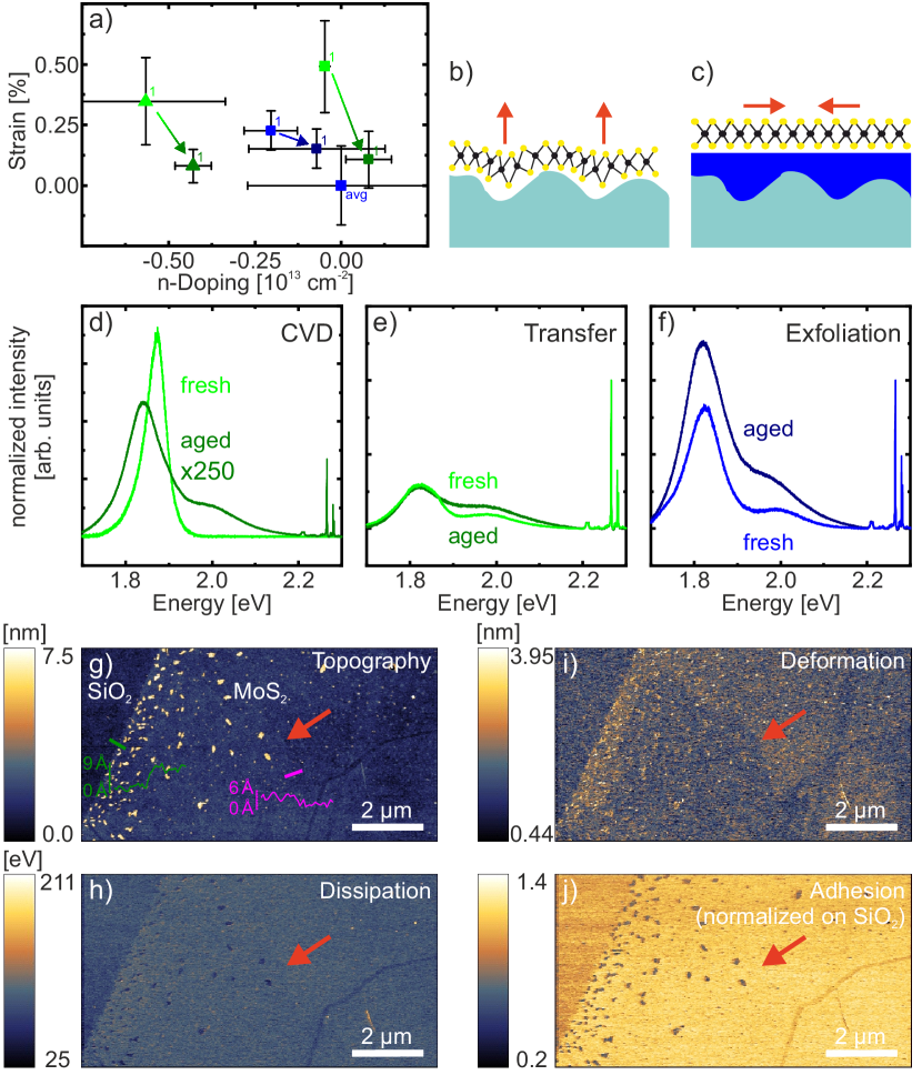
Aging
We start this additional discussion with some observations from a detailed (although non-comprehensive) aging study (Fig. 4). It For this study a CVD grown MoS2 sample with a low defect density (green triangles), a transferred CVD MoS2 sample (green squares), and an exfoliated MoS2 sample (blue squares) were stored for several months under inert nitrogen atmosphere at a humidity of about 20 % to avoid degradation 46. We found that particularly the strain in both CVD based systems was reduced to the level of exfoliated MoS2, while the strain of the exfoliated reference sample remained constant (Fig. 4 (a)). The altered strain in the transferred CVD MoS2 sample towards the strain level of exfoliated MoS2 confirms the hypothesis of strain being introduced by the polymer during the transfer.
A possible explanation is illustrated in Fig. 4 (b) and (c): In transferred MoS2 (Fig. 4 (c)) only in-plane forces are exerted by strain, which let the MoS2 layer relax on its buffer water layer. In contrast, the net forces in CVD MoS2 can be more complex because of the rough substrate (Fig. 4 (b)). When the MoS2 relaxes, channels may form between the MoS2 layer and the substrate, which would be partially filled up with water from the residual humidity. Two additional observations were made in our aging study: (i) The doping level for all sample systems changes only marginally (Fig. 4 (a)), (ii) the PL intensity only changes significantely for CVD MoS2 (green triangles), see Fig. 4 (d)-(f), hence with respect to optoelectronic properties this sample system is most sensitive to storage time. Note: Raman and PL spectra were obtained at different locations and on different flakes of the stored samples, but obviously no spatial variations were detected.
Intercalated Water
To test the hypothesis of the strain reduction mechanism in aged CVD MoS2 we performed AFM measurements shown in Fig. 4 (g)-(j). Here we take advantage of the so-called PeakForce Tapping mode, which allows us to additionally obtain nanomechanical properties such as deformation (Fig. 4 (i)) and adhesion (Fig. 4 (j)). Already when looking at the more common channels topography (Fig. 4 (g)) and dissipation (Fig. 4 (h)) the effect of aging can be clearly seen (red arrow pointing on the same spot in all images). While some parts of the flake are still found to be 0.7 nm thick (green line profile), most areas show a slight increase in height by 2-4 Å (magenta averaged line profile) and exhibit a reduced dissipation (corresponding to a reduction of inelastic deformation by the AFM tip). The nanomechanical data confirms this further because the deformation of MoS2 decreases in those areas. The adhesion force between AFM tip and the MoS2 surface, in contrast, remains constant over the whole sample area. At this point we can exclude the possibility that the contrast changes of the topography, dissipation, and deformation channels are caused by an adsorbate layer on top of the MoS2 layer because adhesion, which is a measure for the force needed to remove the tip from the surface, remains unchanged. Instead, the slightly higher regions are areas of MoS2, underneath which a film of intercalated water already exists. The increase in height by a few Angstroms is in good agreement with the characteristic thickness of a single water molecule layer underneath 2D materials, which was determined to be 0.37 nm 31, 32. The reduced deformation by the AFM tip in this region shows that this water film is incompressible.
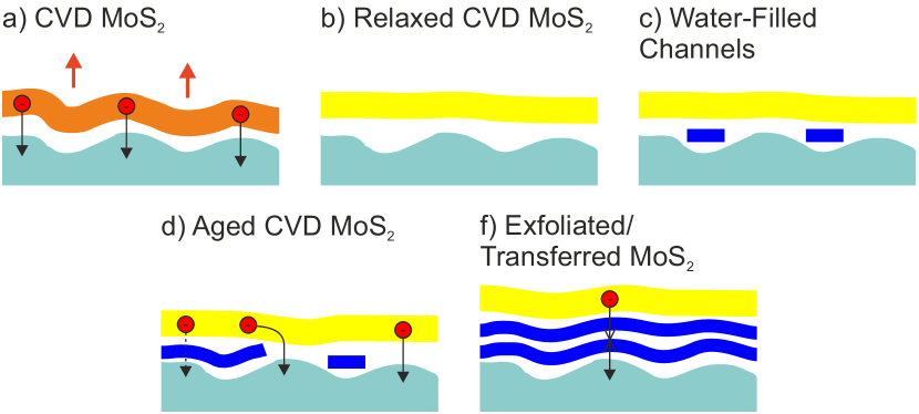
For the water intercalation we propose the following mechanism, which is shown step-by-step in Fig. 5. As grown CVD MoS2 is in direct contact with the rough SiO2 substrate, causing in-plane strain (Fig. 5 (a)). This results in net forces which partially detach the MoS2 layer from the SiO2 substrate and open small channels (Fig. 5 (b)). These channels are subsequently filled with water due to capillary forces (Fig. 5 (c). It is very likely that this filling even supports the channel formation and thus the strain reduction, i.e., step (b) and (c) take place simultaneously. Over time the intercalated water in the channels expands to form water layers underneath the MoS2 (Fig. 5 (d)). The latter stage is observed in the AFM images in Fig. 4 (g)-(j).
If, as with the aged CVD MoS2 sample (green triangle), the water film is non-continuous and/or very thin, charge transfer between MoS2 and substrate may be still present (Fig. 5 (d)). However, if the intercalated water film is continuous and thicker, as in the exfoliated or transferred MoS2-SiO2 system (> 2 water layers of 0.37 nm each, illustration: Fig. 5 (e), AFM data: Fig. 2 (e)), the charge transfer is more efficiently screened resulting in a different doping level in MoS2. A strong PL quenching without a change of the doping level is due to the complex mechanisms which influence the excitons in 2D MoS2. The thin water film, which allows charge transfer between MoS2 and the substrate, may affect the excitons by, e.g., changing the dielectric environment (), which increases the dissociation of excitons 25, probably supported by the exciton diffusion length 47. Nonetheless, PL intensity and doping are obviously not always strictly connected.
MoS2-Graphene Heterostructures
Finally, we have prepared MoS2-graphene heterostructures in order to gain further insight to the screening effect of the intercalated water film underneath transferred single layer MoS2. The heterostructures have been prepared by two different routes, see Fig. 6. Both routes start with CVD graphene (Fig. 6 (a)), which has been transferred from its growth substrate to SiO2 by our recently reported polymer-free transfer technique 48. Afterwards, MoS2 is either transferred onto (Fig. 6 (b)) or grown by CVD on the resulting graphene-SiO2 substrates (Fig. 6 (c) and (d)). In this way, we can compare two different heterostructures: one, where MoS2 is in direct contact with graphene and the second one, where a water film with a comparable thickness to exfoliated or transferred MoS2 on SiO2 is intercalated, see Fig. 2 (a) for illustrations.
The data and resulting properties can be found in Fig.s 1-3 using orange as color and the same convention for the symbol shape as before, i.e. data points for directly grown MoS2 on graphene are represented by the orange triangles and MoS2 transferred on graphene is represented by the orange squares. Note that for both heterostructure types the graphene layer has an increased thickness due to intercalated water (Fig. 2 (e) purple stars), which remains trapped between graphene and SiO2 despite high temperatures during the MoS2 growth process. This is not surprising, as other studies have shown that water intercalated underneath graphene remains trapped after annealing even under UHV conditions 34, 35.
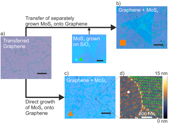
First, we discuss the morpohology of the resulting MoS2-graphene heterostructures. For the transferred heterostructure we obtain large areas (up to a few hundreds of µm2) of optically perfect heterostructures, see Fig. 6 (b). In the case of directly grown MoS2, the whole graphene layer has a more bluish color (Fig. 6 (c)), which is due to MoS2 nanoflakes on the graphene surface as revealed by AFM (Fig. 6 (d)).
These triangular single layer MoS2 nanoflakes grow in a preferred orientation within a given graphene domain (the boundary is marked by the white dotted line). At the domain boundaries a particularly large number of MoS2 flakes is found. It is typical for MoS2 to preferentially grow at imperfections such as step edges as demonstrated for “bulk-graphene” highly oriented pyrolytic graphite (HOPG) substrates 49, 50, 41 and at artificially induced nm-sized defects 51. The oriented growth of MoS2 underlines the cleanliness of the graphene surface after our novel transfer technique 48. It is worth noting, that the MoS2-graphene system based on directly grown MoS2 (orange triangle) has very similar Raman modes in comparison to MoS2 grown on HOPG (brown triangles)41. The similarities of MoS2 grown on HOPG and on graphene (flake size, nucleation at grain boundaries/step edges, orientation, Raman mode positions) confirm the claim that MoS2 on HOPG is a good model system for MoS2 on graphene 49, 41.
Now let us turn to the spectroscopic results. The trend is very similar to the MoS2-SiO2 system, i.e., MoS2-graphene prepared by transfer (orange squares) is more n-doped and less strained than MoS2-graphene grown directly (orange triangles), see Fig. 3. However, there is an offset to the corresponding MoS2-SiO2 systems. It is not surprising that MoS2 in direct contact with graphene has a different doping level than Mos2 in contact with SiO2 because the electronic structures of graphene and SiO2 are very different. Because graphene is reported to be p-doped on SiO2 under ambient conditions 1, 52, it seems likely that graphene affects the doping level MoS2 on top towards p-doping. The fact that MoS2-graphene heterostructure prepared by transfer is less n-doped than MoS2 transferred on SiO2 demonstrates that the intercalated water (due to transfer or exfoliation) may not completely screen the substrate. Some charge transfer is still present i.e. the substrate affects the MoS2 layer despite the intercalated water.
The influence of the substrate (and the role of the intercalated water) can also be seen by the PL intensity of the differently prepared MoS2-graphene heterostructures (Fig. 2 (b)). MoS2 transferred onto graphene (orange triangles) exhibits a PL intensity on the same level of MoS2 transferred or exfoliated onto SiO2 (green, light blue, blue squares), but is doped more like MoS2 grown on SiO2 (green, light blue triangles), see Fig. 3 (b). Obviously the PL intensity of MoS2 is indeed not strictly related to its doping level, but rather to direct environment of the MoS2 layer.
This is even more emphasized in the case of MoS2 directly grown on graphene (orange triangle). Although it is the most p-doped MoS2 system studied in this paper (Fig. 3 (b)) and should thus have an extremely high PL intensity 21, it has the lowest measured PL intensity (Fig. 2 (b)) – even if we take into account that only a fraction of the graphene area is actually covered with single layer MoS2. In this case, the origin of the PL quenching is the dissociation of the excitons by the underlying semimetallic graphene 53, 54, 55. As previously shown for comparable MoSe2-graphene heterostructures, the most efficient charge transfer and thus an even stronger PL quenching is to be expected for a direct coupling between the two van der Waals materials 56. Apparently, the direct growth of MoS2 on graphene via CVD enables such a direct coupling and once more underlines the potential of this fabrication methods also for high quality van der Waals heterostructures.
3 Conclusion
Exfoliated and CVD grown MoS2 monolayers appear extremely different – but this is true only at first glance. The CVD material shows a much more intense PL and the mode positions in its Raman spectra differ significantly from those of the exfoliated material. As a consequence, the usual method for evaluating the number of layers, as described by Lee et al. 29 and established on exfoliated samples is not valid for MoS2 grown by CVD. From our spectroscopic results, conclusions can be drawn about different strain and doping values: CVD grown MoS2 appears to be more strained and less n-doped compared to exfoliated MoS2. However, the actual origin for the apparent differences in PL and Raman is the presence/absence of an intercalated water film. As soon as a water film is present under the CVD grown MoS2, the difference in charge carrier density vanishes. Both, the differences in PL intensity and strain/defect density also become much smaller then. The only difference we could identify is a higher/lower density of non-doping defects in the CVD-grown material. Therefore, we draw the clear conclusion from our data that the intrinsic properties of MoS2 grown by CVD and prepared by exfoliation, respectively, are only marginal.
Our data shows that CVD processes run with MoO3 as precursor typically result in samples with a much larger variation with respect to the strain/defect density values. This indicates the superiority of the AHM precursor for the growth of MoS2 via CVD and leads us to believe that presumably many other 2D TMDCs may be grown with a similarly high quality if the right precursor can be found.
We could show, that MoS2 on graphite is indeed a good model system for the investigation of MoS2-graphene heterostructures. In this case, CVD grown MoS2 interacts much stronger with the substrate. A decoupling by an intercalated water film, as typically occurs after exfoliation or transfer, is not sufficient to ensure that the MoS2 is no longer influenced by the substrate. These findings render heterostructures directly grown via CVD even more promising for energy conversion, sensing, and spintronic devices as one would have expected from proof-of-principle experiments with stacked/transferred van der Waals materials, of which at least one is often exfoliated 57, 58, 59, 60, 61.
4 Methods
4.1 Sample preparation
The single layer MoS2 sheets are either prepared by standard exfoliation technique (scotch tape method) 1, 2 (blue squares in the figures) from a natural bulk MoS2 crystal or by CVD in a three-zone split tube furnace (ThermConcept ROK 70/750/12-3z). Two processes were used: (i) molybdenum trioxide (MoO3) powder as molybdenum source and referred to as MoO3 prcoess in the following (green symbols), and (ii) ammonium heptamolybdate (AHM) as precursor for the molybdenum source in the AHM process (light blue symbols). The used recipes follow:
MoO3 Process
This process is a variation of the classical CVD method developed by Lee et al.3. Two heating zones were used here. A ceramic boat with 50 mg sulfur powder (Sigma Aldrich, 99.98 %) is positioned in the upstream heating zone, a ceramic boat with <1 mg MoO3 powder (Alfa Aesar, 99.95%) and SiO2 susbtrates, which are first cleaned in an ultrasonic bath in ethanol and then treated with perylene-3,4,9,10-tetracarboxylic acid tetrapotassium acid salt (PTAS, 2D semiconductors) as the seeding promoter, is positioned in the adjacent downstream heating zone. After an ambient pressure argon flushing of the tube for 30 minutes at an Ar flow of 50 Ncm3/min, which is maintained for the whole process, the heating zone with the MoO3 powder and the substrates is heated up to a maximum temperature of 750-800 °C with a rate of 1600 °C/h. With a delay of 30 min the sulfur heating zone is heated to 180 °C within 5 min. After a holding time of 25 min at the maximum temperature, the furnace is opened for rapid cooling.
AHM Process
With this process type according to Han et al. 5, the molybdenum source, also in the form of MoO3, is provided in a different way than in the process described above. Instead of adding MoO3 directly into the process system in powder form, it is first produced from water-soluble ammonium heptamolybdate (AHM, Sigma Aldrich) in an additional decomposition step 62, 63. Much less than 1 µL (<< 0.2 mg AHM) is dropleted from a 50:50 mixture of a saturated AHM solution and deionized water onto the previously cleaned substrates and then heated for 30 min at 300 °C to convert AHM to MoO3. In this way, reproducible and smaller quantities of molybdenum can be introduced into the CVD process system. The seeding promoter cholic acid sodium salt (Sigma Aldrich) is then spun on. After positioning the substrate with the molybdenum source in the downstream heating zone and 50 mg sulfur powder in the upstream heating zone the process can be operated as above. However, for the process slightly different optimal parameters were found: Ar flow is hold at 500 Ncm3/min for the whole process (including at least 15 min flushing time, the process and the cooling time). Both heating zones are heated up within 11 minutes to the process temperatures of 150 °C and 750 °C for the heating zone containing the sulfur source and the heating zone containing the the molybdenum source and the substrates respectively. These process temperatures are held for 19 minutes before the furnace is opened for rapid cooling.
Transfer
In order to prepare some of the samples, different transfer techniques are used for the 2D materials MoS2 and graphene (Graphenea). To transfer MoS2, a poly(methyl methacrylate) (PMMA) based wet transfer was used. In detail, a thin PMMA layer (ARP 671.05, Allresist GmbH) was spun on the MoS2 samples and annealed (5 min, 100 °C). In order to remove the PMMA/MoS2 the SiO2 is etched by a KOH solution (0.7 mol/L). After replacing the etching solution with deionized water, the floating PMMA/MoS2 stack is scooped out by another clean SiO2 substrate. The PMMA is removed by an acetone bath. For transferring graphene a polymer free wet transfer is used, which is reported in our previous work 48. In case of growing MoS2 onto the graphene-SiO2 samples, the samples were pre-annealed in activated carbon for 20 min at 100 °C.
4.2 Characterization
Confocal Raman and PL spectroscopy were performed with a Raman microscope (Renishaw InVia) with a laser wavelength of 532 nm and a spot size of 1 µm. Power densities of the laser were typically 0.06 mW/µm2, but had to be reduced by several orders of magnitude for samples with extreme PL intensity to avoid saturation of the detector. Atomic force microscope (AFM) measurements were performed on a Veeco Dimension 3100 AFM in Tapping Mode using Nanosensors PPP-NCHR tips and on a Bruker Dimension Icon in PeakForce Tapping Mode with Bruker ScanAsyst-Air tips. The latter mode is based on the recording of a large number of force-distance curves, thus allowing the simultaneous spatial resolution of mechanical properties (deformation, adhesion, …) in addition to topography.
The authors acknowledge support from the German Research Foundation (DFG) by funding SCHL 384/20-1 (project number 406129719). PeakForce AFM, Raman and PL spectroscopy was performed at the Interdisciplinary Center for Analytics on the Nanoscale (ICAN), a core facility funded by the German Research Foundation (DFG, reference RI_00313).
The following files are available free of charge.
-
•
Supplementary Material - MoS2 CVD vs Exfoliation: More AFM images for exemplary MoS2 thickness and substrate roughness evaluation, additional PeakForce AFM channel
References
- Novoselov et al. 2004 Novoselov, K. S.; Geim, A. K.; Morozov, S. V.; Jiang, D.; Zhang, Y.; Dubonos, S. V.; Grigorieva, I. V.; Frisov, A. A. Electric Field Effect in Atomically Thin Carbon Films. Science 2004, 306, 666–669
- Novoselov et al. 2005 Novoselov, K. S.; Jiang, D.; Schedin, F.; Khotkevich, V. V.; Morozov, S. V.; Geim, A. K. Two-Dimensional Atomic Crystals. Proc. Natl. Acad. Sci. U. S. A. 2005, 102, 10451–10453
- Lee et al. 2012 Lee, Y.-H.; Zhang, X.-Q.; Zhang, W.; Chang, M.-T.; Lin, C.-T.; Chang, K.-D.; Yu, Y.-C.; Wang, J. T.-W.; Chang, C.-S.; Li, L.-J.; Lin, T.-W. Synthesis of Large-Area MoS2 Atomic Layers with Chemical Vapour Depostion. Adv. Mater. 2012, 24, 2320–2325
- Dumcenco et al. 2015 Dumcenco, D.; Ovchinnikov, D.; Marinov, K.; Lazić, P.; Gibertini, M.; Marzari, N.; Lopez Sanchez, O.; Kung, Y.-C.; Krasnozhon, D.; Chen, M.-W.; Bertolazzi, S.; Gillet, P.; Fontcuberta i Morral, A.; Radenovic, A.; Kis, A. Large-Area Epitaxial Monolayer MoS2. ACS Nano 2015, 9, 4611–4620
- Han et al. 2015 Han, G. H.; Kybert, N. J.; Naylor, C. H.; Lee, B. S.; Ping, J.; Park, J. H.; Kang, J.; Lee, S. Y.; Lee, Y. H.; Agarwal, R.; Johnson, A. T. C. Seeded Growth of Highly Crystalline Molybdenum Disulphide Monolayers at Controlled Locations. Nat. Commun. 2015, 6, 6128
- Hong et al. 2015 Hong, J. et al. Exploring Atomic Defects in Molybdenum Disulphide Monolayers. Nat. Commun. 2015, 6, 6293
- Rice et al. 2013 Rice, C.; Young, R. J.; Zan, R.; Bangert, U.; Wolverson, D.; Georgiou, T.; Jalil, R.; Novoselov, K. S. Raman-Scattering Measurements and First-Principles Calculations of Strain-Induced Phonon Shifts in Monolayer MoS2. Phys. Rev. B 2013, 87, 081307
- Wang et al. 2013 Wang, Y.; Cong, C.; Qiu, C.; Yu, T. Raman Spectroscopy Study of Lattice Vibration and Crystallographic Orientation of Monolayer MoS2 under Uniaxial Strain. Small 2013, 9, 2857–2861
- Conley et al. 2013 Conley, H. J.; Wang, B.; Ziegler, J. I.; Haglund, R. F.; Pantelides, S. T.; Bolotin, K. I. Bandgap Engineering of Strained Monolayer and Bilayer MoS2. Nano Lett. 2013, 13, 3626–3630
- Castellanos-Gomez et al. 2013 Castellanos-Gomez, A.; Roldán, R.; Cappelluti, E.; Buscema, M.; Guinea, F.; van der Zant, H. S. J.; Steele, G. A. Local Strain Engineering in Atomically Thin MoS2. Nano Lett. 2013, 13, 5361–5366
- Scheuschner et al. 2014 Scheuschner, N.; Ochedowski, O.; Kaulitz, A.-M.; Gillen, R.; Schleberger, M.; Maultzsch, J. Photoluminescence of Freestanding Single- and Few-Layer MoS2. Phys. Rev. B 2014, 89, 125406
- Lloyd et al. 2016 Lloyd, D.; Liu, X.; Christopher, J. W.; Cantley, L.; Wadehra, A.; Kim, B. L.; Goldberg, B. B.; Swan, A. K.; Bunch, J. S. Band Gap Engineering with Ultralarge Biaxial Strains in Suspended Monolayer MoS2. Nano Lett. 2016, 16, 5836–5841
- Kukucska and Koltai 2017 Kukucska, G.; Koltai, J. Theoretical Investigation of Strain and Doping on the Raman Spectra of Monolayer MoS2. Phys. Status Solidi B 2017, 254, 1700184
- Christopher et al. 2019 Christopher, J. W.; Vutukuru, M.; Lloyd, D.; Bunch, J. S.; Goldberg, B. B.; Bishop, D. J.; Swan, A. K. Monolayer MoS2 Strained to 1.3% With a Microelectromechanical System. J. Microelectromech. Syst. 2019, 28, 254–263
- Chakraborty et al. 2012 Chakraborty, B.; Bera, A.; Muthu, D. V. S.; Bhowmick, S.; Waghmare, U. V.; Sood, A. K. Symmetry-Dependent Phonon Renormalization in Monolayer MoS2 Transistor. Phys. Rev. B 2012, 85, 161403
- Michail et al. 2016 Michail, A.; Delikoukos, N.; Parthenios, J.; Galiotis, C.; Papagelis, K. Optical Detection of Strain and Doping Inhomogeneities in Single Layer MoS2. Appl. Phys. Lett. 2016, 108, 173102
- Chae et al. 2017 Chae, W. H.; Cain, J. D.; Hanson, E. D.; Murthy, A. A.; Dravid, V. P. Substrate-Induced Strain and Charge Doping in CVD-Grown Monolayer MoS2. Appl. Phys. Lett. 2017, 111, 143106
- Dubey et al. 2017 Dubey, S. et al. Weakly Trapped, Charged, and Free Excitons in Single-Layer MoS2 in the Presence of Defects, Strain, and Charged Impurities. ACS Nano 2017, 11, 11206–11216
- Mak et al. 2010 Mak, K. F.; Lee, C.; Hone, J.; Shan, J.; Heinz, T. F. Atomically Thin MoS2: A New Direct-Gap Semiconductor. Phys. Rev. Lett. 2010, 105, 136805
- Splendiani et al. 2010 Splendiani, A.; Sun, L.; Zhang, Y.; Li, T.; Kim, J.; Chim, C.-Y.; Galli, G.; Wang, F. Emerging Photoluminescence in Monolayer MoS2. Nano Lett. 2010, 10, 1271–1275
- Mak et al. 2013 Mak, K. F.; He, K.; Lee, C.; Lee, G. H.; Hone, J.; Heinz, T. F.; Shan, J. Tightly Bound Trions in Monolayer MoS2. Nat. Mater. 2013, 12, 207–211
- Tongay et al. 2013 Tongay, S.; Suh, J.; Ataca, C.; Fan, W.; Luce, A.; Kang, J. S.; Liu, J.; Ko, C.; Raghunathanan, R.; Zhou, J.; Ogletree, F.; Li, J.; Grossman, J. C.; Wu, J. Defects Activated Photoluminescence in Two-dimensional Semiconductors: Interplay between Bound, Charged, and Free Excitons. Sci. Rep. 2013, 3, 2657
- Nan et al. 2014 Nan, H.; Wang, Z.; Wang, W.; Liang, Z.; Lu, Y.; Chen, Q.; He, D.; Tan, P.; Miao, F.; Wang, X.; Wang, J.; Ni, Z. Strong Photoluminescence Enhancement of MoS2 through Defect Engineering and Oxygen Bonding. ACS Nano 2014, 8, 5738–5745
- Frisenda et al. 2017 Frisenda, R.; Drüppel, M.; Schmidt, R.; Michaelis de Vasconcellos, S.; Perez de Lara, D.; Bratschitsch, R.; Rohlfing, M.; Castellanos-Gomez, A. Biaxial Strain Tuning of the Optical Properties of Single-Layer Transition Metal Dichalcogenides. npj 2D Mater. Appl. 2017, 1, 10
- Steinhoff et al. 2017 Steinhoff, A.; Florian, M.; Rösner, M.; Schönhoff, G.; Wehling, T. O.; Jahnke, F. Exciton Fission in Monolayer Transition Metal Dichalcogenide Semiconductors. Nat. Commun. 2017, 8, 1166
- Kaplan et al. 2016 Kaplan, D.; Gong, Y.; Mills, K.; Swaminathan, V.; Ajayan, P. M.; Shirodkar, S.; Kaxiras, E. Excitation Intensity Dependence of Photoluminescence from Monolayers of MoS2 and WS2/MoS2 Heterostructures. 2D Mater. 2016, 3, 015005
- Chen et al. 2017 Chen, F.; Wang, L.; Wang, T.; Ji, X. Enhanced Local Photoluminescence of a Multilayer MoS2 Nanodot Stacked on Monolayer MoS2 Flakes. Opt. Mater. Express 2017, 7, 1365–1373
- Lin et al. 2014 Lin, Y.; Ling, X.; Yu, L.; Huang, S.; Hsu, A. L.; Lee, Y.-H.; Kong, J.; Dresselhaus, M. S.; Palacios, T. Dielectric Screening of Excitons and Trions in Single-Layer MoS2. Nano Lett. 2014, 14, 5569–5576
- Lee et al. 2010 Lee, C.; Yan, H.; Brus, L. E.; Heinz, T. F.; Hone, J.; Ryu, S. Anomalous Lattice Vibrations of Single- and Few-Layer MoS2. ACS Nano 2010, 4, 2695–2700
- Kuc et al. 2011 Kuc, A.; Zibouche, N.; Heine, T. Influence of Quantum Confinement on the Electronic Structure of the Transition Metal Sulfide TS2. Phys. Rev. B 2011, 83, 244059
- Xu et al. 2010 Xu, K.; Peigen, C.; Heath, J. R. Graphene Visualizes the First Water Adlayers on Mica at Ambient Conditions. Science 2010, 329, 1188–1191
- Komurasaki et al. 2012 Komurasaki, H.; Tsukamoto, T.; Yamazaki, K.; Ogino, T. Layered Structures of Interfacial Water and Their Effects on Raman Spectra in Graphene-on-Sapphire Systems. J. Phys. Chem. C 2012, 116, 10084–10089
- Ochedowski et al. 2013 Ochedowski, O.; Kleine Bussmann, B.; Ban d’Etat, B.; Lebius, H.; Schleberger, M. Manipulation of the Graphene Surface Potential by Ion Irradiation. Appl. Phys. Lett. 2013, 102, 153103
- Ochedowski et al. 2014 Ochedowski, O.; Bussmann, B. K.; Schleberger, M. Graphene on Mica - Intercalated Water Trapped for Life. Sci. Rep. 2014, 4, 6003
- Temmen et al. 2014 Temmen, M.; Ochedowski, O.; Schleberger, M.; Reichling, M.; Bollmann, T. R. J. Hydration Layers Trapped between Graphene and a Hydrophilic Substrate. New J. Phys. 2014, 16, 053039
- Varghese et al. 2015 Varghese, J. O.; Agbo, P.; Sutherland, A. M.; Brar, V. W.; Rossman, G. R.; Gray, H. B.; Heath, J. R. The Influence of Water on the Optical Properties of Single-Layer Molybdenum Disulfide. Adv. Mater. 2015, 27, 2734–2740
- Lin et al. 2015 Lin, Z.; Zhao, Y.; Zhou, C.; Zhong, R.; Wang, X.; Tsang, Y. H.; Chai, Y. Controllable Growth of Large-Size Crystalline MoS2 and Resist-Free Transfer Assisted with a Cu Thin Film. Sci. Rep. 2015, 5, 18596
- Deng et al. 2017 Deng, S.; Gao, E.; Xu, Z.; Berry, V. Adhesion Energy of MoS2 Thin Films on Silicon-Based Substrates Determined via the Attributes of a Single MoS2 Wrinkle. ACS Appl. Mater. Interfaces 2017, 9, 7812–7818
- Pollmann et al. 2018 Pollmann, E.; Madauß, L.; Zeuner, V.; Schleberger, M. Strain in Single-Layer MoS2 Flakes Grown by Chemical Vapor Deposition. Wandelt, K., (Ed.) Encyclopedia of Interfacial Chemistry: Surface Science and Electrochemistry 2018, 338–343
- Deng et al. 2019 Deng, S.; Che, S.; Debbarma, R.; Berry, V. Strain in a Single Wrinkle on an MoS2 Flake for In-Plane Realignment of Band Structure for Enhanced Photo-Response. Nanoscale 2019, 11, 504–511
- Pollmann et al. 2020 Pollmann, E.; Morbec, J. M.; Madauß, L.; Bröckers, L.; Kratzer, P.; Schleberger, M. Molybdenum Disulphide Nanoflakes Grown by Chemical Vapour Deposition on Graphite: Nucleation, Orientation, and Charge Transfer. J. Phys. Chem. C 2020, 124, 2689–2697
- Buscema et al. 2014 Buscema, M.; Steele, G. A.; van der Zant, H. S. J.; Castellanos-Gomez, A. The Effect of the Substrate on the Raman and Photoluminescence Emission of Single-Layer MoS2. Nano Res. 2014, 7, 561–571
- Parkin et al. 2016 Parkin, W. M.; Balan, A.; Liang, L.; Das, P. M.; Lamparski, M.; Naylor, C. H.; Rodríguez-Manzo, J. A.; Johnson, A. T. C.; Meunier, V.; Drndić, M. Raman Shifts in Electron-Irradiated Monolayer MoS2. ACS Nano 2016, 10, 4134–4142
- Madauß et al. 2018 Madauß, L. et al. Highly Active Single-Layer MoS2 Catalysts Synthesized by Swift Heavy Ion Irradiation. Nanoscale 2018, 10, 22908–22916
- Komsa and Krasheninnikov 2015 Komsa, H.-P.; Krasheninnikov, A. V. Native Defects in Bulk and Monolayer MoS2 from First Principles. Phys. Rev. B 2015, 91, 125304
- Gao et al. 2016 Gao, J.; Li, B.; Tan, J.; Chow, P.; Lu, T.-M.; Koratkar, N. Aging of Transition Metal Dichalcogenide Monolayers. ACS Nano 2016, 10, 2628–2635
- Wang et al. 2012 Wang, R.; Ruzicka, B. A.; Kumar, N.; Bellus, M. Z.; Chiu, H.-Y.; Zhao, H. Ultrafast and Spatially Resolved Studies of Charge Carriers in Atomically Thin Molybdenum Disulfide. Phys. Rev. B 2012, 86, 045406
- 48 Madauß, L.; Pollmann, E.; Foller, T.; Schumacher, J.; Hagemann, U.; Heckhoff, T.; Herder, M.; Skopinski, L.; Breuer, L.; Hierzenberger, A.; Wittmar, A.; Lebius, H.; Ulbricht, M.; Joshi, R.; Schleberger, M. A Swift Technique to Hydrophobize Graphene and Increase its Mechanical Stability and Charge Carrier Density. npj 2D Mater. Appl. accepted
- Koós et al. 2016 Koós, A. A.; Vancsó, P.; Magda, G. Z.; Osváth, Z.; Kertész, K.; Dobrik, G.; Hwang, C.; Tapasztó, L.; Biró, L. P. STM Study of the MoS2 Flakes Grown on Graphite: A Model System for Atomically Clean 2D Heterostructure Interfaces. Carbon 2016, 105, 408–415
- Lu et al. 2015 Lu, C.-I.; Butler, C. J.; Huang, J.-K.; Hsing, C.-R.; Yang, H.-H.; Chu, Y.-H.; Luo, C.-H.; Sun, Y.-C.; Hsu, S.-H.; Yang, K.-H. O.; Wei, C.-M.; Li, L.-J.; Lin, M.-T. Graphite Edge Controlled Registration of Monolayer MoS2 Crystal Orientation. Appl. Phys. Lett. 2015, 106, 181904
- Pollmann et al. 2018 Pollmann, E.; Ernst, P.; Madauß, L.; Schleberger, M. Ion-Mediated Growth of Ultra Thin Molybdenum Disulfide Layers on Highly Oriented Pyrolytic Graphite. Surf. Coat. Technol. 2018, 349, 783–786
- Ernst et al. 2016 Ernst, P.; Kozubek, R.; Madauß, L.; Sonntag, J.; Lorke, A.; Schleberger, M. Irradiation of Graphene Field Effect Transistors with Highly Charged Ions. Nucl. Instrum. Methods Phys. Res. B 2016, 382, 71–75
- Pierucci et al. 2016 Pierucci, D.; Henck, H.; Naylor, C. H.; Sediri, H.; Lhuillier, E.; Balan, A.; Rault, J. E.; Dappe, Y. J.; Bertran, F.; Le Fèvre, P.; Johnson, A. T. C.; Ouerghi, A. Large Area Molybdenum Disulphide-Epitaxial Graphene Vertical Van der Waals Heterostructures. Sci. Rep. 2016, 6, 26656
- Zhang et al. 2014 Zhang, W.; Chuu, C.-P.; Huang, J.-K.; Chen, C.-H.; Tsai, M.-L.; Chang, Y.-H.; Liang, C.-T.; Chen, Y.-Z.; Chueh, Y.-L.; He, J.-H.; Chou, M.-Y.; Li, L.-J. Ultrahigh-Gain Photodetectors Based on Atomically Thin Graphene-MoS2 Heterostructures. Sci. Rep. 2014, 4, 3826
- Huo et al. 2015 Huo, N.; Wei, Z.; Meng, X.; Kang, J.; Wu, F.; Li, S.-S.; Wei, S.-H.; Li, J. Interlayer Coupling and Optoelectronic Properties of Ultrathin Two-Dimensional Heterostructures Based on Graphene, MoS2 and WS2. J. Mater. Chem. C 2015, 3, 5467–5473
- Froehlicher et al. 2018 Froehlicher, G.; Lorchat, E.; Berciaud, S. Charge Versus Energy Transfer in Atomically Thin Graphene-Transition Metal Dichalcogenide van der Waals Heterostructures. Phys. Rev. X 2018, 8, 011007
- Dankert and Dash 2017 Dankert, A.; Dash, S. P. Electrical Gate Control of Spin Current in van der Waals Heterostructures at Room Temperature. Nat. Commun. 2017, 8, 16093
- Roy et al. 2013 Roy, K.; Padmanabhan, M.; Goswami, S.; Sai, T. P.; Kaushal, S.; Ghosh, A. Optically Active Heterostructures of Graphene and Ultrathin MoS2. Solid State Commun. 2013, 175-176, 35–42
- Yu et al. 2013 Yu, W. J.; Liu, Y.; Zhou, H.; Yin, A.; Li, Z.; Huang, Y.; Duan, X. Highly Efficient Gate-Tunable Photocurrent Generation in Vertical Heterostructures of Layered Materials. Nat. Nanotechnol. 2013, 8, 952–958
- Cho et al. 2015 Cho, B.; Yoon, J.; Lim, S. K.; Kim, A. R.; Kim, D.-H.; Park, S.-G.; Kwon, J.-D.; Lee, Y.-J.; Lee, K.-H.; Lee, B. H.; Ko, H. C.; Hahm, M. G. Chemical Sensing of 2D Graphene/MoS2 Heterostructure Device. ACS Appl. Mater. Interfaces 2015, 7, 16775–16780
- Zhao et al. 2018 Zhao, M.; Song, P.; Teng, J. Electrically and Optically Tunable Responses in Graphene/Transition-Metal-Dichalcogenide Heterostructures. ACS Appl. Mater. Interfaces 2018, 10, 44102–44108
- Hanafi et al. 1981 Hanafi, Z. M.; Khilla, M. A.; Askar, M. H. The Thermal Decomposition of Ammonium Heptamolybdate. Thermochim. Acta 1981, 45, 221–232
- Wienold et al. 2003 Wienold, J.; Jentoft, R. E.; Ressler, T. Structural Investigation of the Thermal Decomposition of Ammonium Heptamolybdate by in situ XAFS and XRD. Eur. J. Inorg. Chem. 2003, 6, 1058–1071
TOC Graphic
![[Uncaptioned image]](/html/2006.05789/assets/x7.png)