Decoupling Molybdenum Disulfide from its Substrate by Cesium Intercalation
Abstract
Intercalation of alkali atoms within the lamellar transition metal dichalcogenides is a possible route toward a new generation of batteries. It is also a way to induce structural phase transitions authorizing the realization of optical and electrical switches in this class of materials. The process of intercalation has been mostly studied in three-dimensional dichalcogenide films. Here, we address the case of a single-layer of molybdenum disulfide (MoS2), deposited on a gold substrate, and intercalated with cesium (Cs) in ultra-clean conditions (ultrahigh vacuum). We show that intercalation decouples MoS2 from its substrate. We reveal electron transfer from Cs to MoS2, relative changes in the energy of the valence band maxima, and electronic disorder induced by structural disorder in the intercalated Cs layer. Besides, we find an abnormal lattice expansion of MoS2, which we relate to immediate vicinity of Cs. Intercalation is thermally activated, and so is the reverse process of de-intercalation. Our work opens the route to a microscopic understanding of a process of relevance in several possible future technologies, and shows a way to manipulate the properties of two-dimensional dichalcogenides by "under-cover" functionalization.
keywords:
Molybdenum Disulfide, Intercalation, Scanning Tunneling Microscopy, Surface X-ray Diffraction, Density functional theoryUniv. Grenoble Alpes, CNRS, Grenoble INP, Institut NEEL, 38000 Grenoble, France \alsoaffiliationESRF, The European Synchrotron, 38043 Grenoble, France
1 Introduction
The interest for transition metal dichalcogenide single-layers, initially spurred by the bright light emission found in molybdenum disulfide (MoS2) 1, 2 and the achievement of electrostatic switching of electrical conduction in MoS2,3 has revived activities devoted to the synthesis of these materials. Efforts to elaborate them with a structural quality similar to the one obtained in mechanically exfoliated samples with bottom-up approaches – chemical vapour deposition, 4, 5, 6, 7 chalcogenation of metal surfaces,8, 9, 10 or molecular beam epitaxy, standard11 or reactive under H2S atmosphere12, 13, 14 – are ongoing. Both chalcogenation and reactive molecular beam epitaxy usually require a metallic substrate. As-prepared samples are hence not suited to the study of some of the key properties of the material, e.g. those related to excitons which become very short-lived due to the immediate vicinity of a metallic (substrate) charge reservoir, and electrical transport properties which are shunt by the conductive substrate. Besides, in the prototypical case of Au(111) as a substrate, MoS2 does not retain the properties of the isolated material. Significant interaction between the electronic bands of MoS2 and Au(111) was indeed detected15 and the existence of a moiré pattern was found to induce a nanometer-scale modulation of this interaction.16
One way to alter this interaction is to "lift" MoS2 from its surface. Actually, such lifting occurs spontaneously, across regions spanning typically a nanometer, when MoS2 overhangs on Ångström-deep vacancy islands of the substrate.17 Effective lifting may be achieved using an alternative strategy, namely by intercalating a layer of a species decoupling MoS2 from its substrate. This strategy, which allowed to obtain quasi-free-standing graphene18, 19 (another two-dimensional material), has been explored recently with single-layer WS2,20 but not with single-layer MoS2 so far, to our knowledge.
On the contrary, intercalation of thicker transition metal dichalcogenides has been thoroughly investigated. Much like with graphite, a rich variety of systems with modulated structure in the direction perpendicular to the basal plane can be formed this way.21 Using layers of alkali atoms, molecules, or transition metals as intercalants, unique properties including superconductivity and (anti)ferromagnetism have been found.21 The ability to store (release) alkali atoms by intercalation (de-intercalation) also makes transition metal dichalcogenides possible electrode materials, both as cathode22 and anode,23, 24, 25 for Li-ion batteries. Electro-donor intercalants promote a structural phase transition from a semiconducting phase to a metallic one,26, 27, 28, 29, 30, 31, 32, 33, 34, 35 with potential applications in data storage and reconfigurable electrical circuitry.
Here, we report on the intercalation and de-intercalation of the alkali cesium (Cs) atoms. Unlike all works addressing in-solution intercalation of bulk-like transition metal dichalcogenide layers, the focus of our work is on single-layer MoS2 flakes, prepared on Au(111), and (de)intercalated under ultrahigh vacuum conditions. We find that the process of intercalation is thermally activated, being completed after few tens of minutes at a temperature of 550 K. Above 850 K, deintercalation is efficient and completed within a few tens of minutes. Intercalated cesium forms a a Cs monolayer with an ill-ordered structure compatible with a reconstruction with respect to Au(111). We reveal electron transfer from Cs to MoS2, modifications of the relative positions of the valence band maxima in MoS2, and electronic disorder induced by structural disorder in the intercalated layer. Upon intercalation, MoS2 is lifted, and adopts an unusually large lattice parameter. Our analysis combines scanning tunneling microscopy (STM), reflection high-energy electron diffraction (RHEED), grazing incidence X-ray diffraction (GIXRD), reflectivity (XRR), X-ray photoelectron spectroscopy (XPS), and angle-resolved photoemission spectroscopy (ARPES) all performed under ultrahigh vacuum, in some cases in operando during intercalation. Further insights are brought by density functional theory (DFT) calculations.
2 Methods
Three ultrahigh vacuum systems were used for our experiments. A first one is coupled to the X-ray synchrotron beam delivered at the BM32 beamline of the ESRF. It has a base pressure of 310-10 mbar and is equipped with a quartz micro-balance and a RHEED apparatus. The second one, at Institut Néel (Grenoble), with a base pressure of 210-10 mbar, is part of a larger ultrahigh vacuum system comprising a STM, a RHEED apparatus, and a quartz microbalance. The samples were prepared in each system before being investigated by RHEED, STM, GIXRD, and XRR. Temperatures were measured with a pyrometer in both systems. Note that the pyrometers and the chamber configurations are different in the two systems, which implies a plausible variability (50 K) in the measurements, and suggests caution when comparing these measurements. The third ultrahigh vacuum system is installed at the SGM-3 endstation36 of the ASTRID2 synchrotron radiation source (Aarhus); it includes one chamber (base pressure 10-10 mbar) devoted to ARPES and XPS measurements, and two other chambers (base pressures, 410-10 mbar) comprising a STM. All three ultrahigh vacuum systems are equipped with a Cs evaporator. MoS2/Au(111) was prepared in Grenoble and transported in atmospheric conditions to Aarhus where it was degassed in ultrahigh vacuum at 500 K. There, temperatures were measured using a K type thermocouple fixed on the rear side of the Au (111) crystal. The cleanliness of the surface was confirmed with STM and photoelectron spectroscopy.
Single-crystals bought from Surface Preparation Laboratory and Mateck were prepared under ultrahigh vacuum by repeated cycles of room temperature sputtering with 0.8-1 keV Ar+ ions and annealing to 900 K. Surface cleanliness was checked with STM imaging and RHEED, both revealing a well-developped herringbone reconstruction. Molybdenum was evaporated using a high-purity rod heated by electron-beam bombardment, at a rate of 0.02 monolayer/min in the ultrahigh vacuum chamber coupled to the X-ray beam and in the ultrahigh vacuum chamber coupled to the STM, respectively (one monolayer referring to the surface coverage of a single-layer MoS2 on Au(111)). This rate was determined with both a quartz microbalance and STM. For introduction of H2S in the ultrahigh vacuum chambers, we used an automatic injection system by VEGATEC that supplies H2S via pneumatic valves (chamber coupled to the X-ray beam), and a leak-valve (chamber coupled to the STM). The latter system comprises large copper parts. Their surface was saturated by maintaining a pressure of 10-6 mbar of H2S for 30 min. Without this treatment, residual gas analysis revealed that H2S was prominently decomposed before even reaching the sample surface, which prevented MoS2 growth.
Cesium was deposited under ultrahigh vacuum by resistive heating of a high purity Cs dispenser (SAES Getter). Assessing the deposited Cs dose is not a straightforward task. Cesium dose measurements, using a quartz microbalance for instance, are seldom reported. Exceptions include low temperature measurements;37 in contrast, our room temperature measurements were inconclusive. Alternative calibration methods were hence needed. In the ultrahigh vacuum system where STM imaging was performed, graphene growth on Ir(111) is operative. Cesium deposition in this system leads to its intercalation between graphene and Ir(111) in a sequence of well-crystallized phases readily detected with electron diffraction.38 At fixed current flowing the Cs dispenser (6.5 A) we hence determined the deposition time required for the onset of a Cs reconstruction relative to the graphene lattice, which corresponds to a well-defined Cs density. Using this calibration, we deposited Cs in two steps, each at room temperature followed by a 500 K annealing, with a total nominal Cs quantity equivalent to 0.7 Cs atoms per Au atom on the surface. In the ultrahigh vacuum system were XPS and ARPES data were acquired, a second calibration method was used. Cesium was deposited (5.7 A current) for a given time at room temperature onto Au(111), and the Cs density was assessed by comparing the area under the Cs peaks and Au surface 4 components in XPS, assuming that Cs is in the form of a flat sub-monolayer deposit. With this calibration at hand, we then deposited Cs in two steps, each at room temperature followed by 550 K annealing, corresponding nominally to 0.3 and 0.6 Cs atoms per Au atom on the surface. In the third ultrahigh vacuum system, installed at the BM32 beamline, we could not use any of these two methods. We hence decided to deposit a large excess of Cs, using a high current flowing the Cs dispenser (7.2 A) and large deposition times, each of 30 min. There also we deposited Cs sequentially, in three steps, each at room temperature followed by a 500 K annealing.
Diffraction measurements were performed at European Synchrotron Radiation Facility using a -axis diffractometer installed at the BM32 CRG/IF beamline and optimized for grazing incidence surface X-ray diffraction. The experimental energy was set at 11.8 keV, below the Au absorption edge. The incident angle was set to 0.24∘, slightly below the critical angle for total external reflection, to enhance the signal from MoS2 while minimizing the background. The diffraction signal was acquired with a Maxipix two-dimensional detector (2561288 pixels, each of size 55 m).
The XRR spectra were processed with PyRod (home-made software for surface diffraction 2D data treatment). Data were integrated in reciprocal space and the profiles were extracted as a function of the modulus of the scattering vector perpendicular to the surface (). Corrections to this integrated intensity were applied for beam polarization, surface active area and gaussian beam profile. Correction for beam refraction at interfaces were used to calculate inside the sample. The ANA-ROD software39 was used for modeling the surface structure of the samples and fitting the XRR data.
The STM data we show were acquired in Grenoble with an Omicron STM-1 apparatus, at room temperature under ultrahigh vacuum, in a dedicated chamber with a base pressure of 510-11 mbar. At the SGM-3 endstation, an Aarhus STM was used to check the sample quality after Cs deposition, which gave consistent results with those obtained in Grenoble.
ARPES and XPS measurements were performed at the SGM-3 end station of the ASTRID2 synchrotron radiation source.36 The ARPES and XPS data were collected at room temperature at photon energies of 49 eV and 130 eV respectively. The energy and angular resolutions were better than 20 meV and 0.2∘ respectively.
Structural relaxations as well as electronic structure determination have been performed using DFT. The DFT localized-orbital molecular-dynamics code as implemented in Fireball40, 41, 42 has been used to optimize the MoS2/Au(111) and the MoS2/Cs/Au(111) structures or to determine their corresponding electronic properties. Standard previously used basis sets have been considered for Mo, S and Au,43 and an basis set with cut-off radii of 6.8 (in atomic units), has been considered for Cs. A hexagonal slab of 77 Au atoms with five layers in the plane, and a topmost 66 MoS2 have been used to model the MoS2/Au(111) interface. This configuration has been optimized until the forces become less than 0.1 eV/Å. The bottom two Au layers were fixed to simulate the Au bulk for the MoS2/Au(111) interface. The MoS2/Cs/Au(111) system, with a Cs reconstruction on Au(111) requires a large supercell to be treated. In this systems, the atomic positions were fixed to the average values derived from the analysis of the XRR data. We have used a set of 32 -points in the plane for self-consistency and density of states calculations.
3 Results and Discussion
Single-layer MoS2 flakes were grown following the procedure described by Grønborg et al.44 In short, the clean Au(111) surface was exposed to a partial pressure of H2S () introduced in the ultrahigh vacuum systems, then molybdenum was deposited on the surface in presence of H2S, and the sample was annealed to 900 K without the Mo atomic beam but still in presence of H2S. This sequence was repeated several times to adjust the surface coverage with MoS2. In the two ultrahigh vacuum chambers where MoS2 was grown, we used = 10-5 and 10-6 mbar respectively. Figure 1a-d shows the typical diffraction patterns and morphology of the surface after growth. The MoS2 flakes exhibit straight edges,45 have an extension of the order of several 10 nm; in between the flakes the herringbone reconstruction of the bare Au(111) is visible. The fraction of the surface covered with MoS2 was 7015%, 285%, and 2515% (as determined from the nominal amount of Mo deposited on the surface, or with STM whenever possible) for the samples studied with GIXRD/XRR, STM, and XPS/ARPES, respectively. Our STM observations are consistent with those in previous reports.13, 44
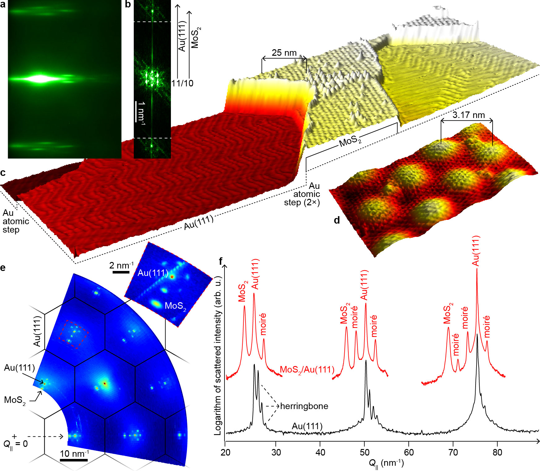
Structure of MoS2 single-layer islands on Au(111). A pronounced pattern, with 3.170.01 nm periodicity, is visible on the MoS2 flakes presented in Figure 1c,d. This pattern arises from the lattice mismatch between MoS2 and the substrate, and is described with an analogy to the optical moiré effect.13 Careful analysis of atomically-resolved STM images and their Fourier transform (Figure 1b) allows to determine the size of the moiré unit cell. For the example shown in Figure 1, we find that the highest symmetry Au(111) and MoS2 crystallographic directions are precisely aligned, and that the unit cell corresponds to the coincidence of 10 MoS2 unit cells onto 11 Au(111) unit cells (1011), consistent with a recent report.14
This moiré unit cell is varying from one MoS2 island to another. The average reciprocal space lattice vector associated to the moiré is directly inferred from RHEED (Figure 1a) and GIXRD (Figure 1e,f) data by measuring the relative positions of the moiré or MoS2 peaks with respect to the Au(111) peaks, to be 1.884 0.001 nm-1.
The full-width at half maximum of the MoS2 peaks in a radial direction (Figure 1f) increases from 0.32 0.05 nm-1 to 0.51 0.05 nm-1 from first to third order. This corresponds to a domain size of about 20 nm and a distribution of in-plane lattice parameter of typically 0.6%.46 Strikingly, the domain size is here smaller than the value of several 10 nm corresponding to the flake size that we determined by visual inspection of STM images. This difference simply shows that the flakes are not single-crystal, and actually consist each of (smaller) single-crystal grains. As discussed in the Supporting Information (SI), we indeed frequently observe linear defects within the flakes, at the boundary between laterally-shifted domains within the flake (see Figure S1). Our interpretation is that at each of the several steps of the MoS2 cyclic preparation, new MoS2 islands nucleate, grow, and coalesce with pre-existing ones – no lattice re-organisation occurs that would eliminate the linear defect (so-called out-of-phase grain boundaries) to yield large single-crystal flakes.
To model the structure of MoS2 and learn more about the out-of-plane structure of the material, we use DFT calculations taking van der Waals interactions into account. For that purpose, we choose an unsheared moiré unit cell with 6 MoS2 units matching 7 Au(111) surface units. This (67) coincidence lattice is not the (1011) observed experimentally. Our choice is however legitimate since in our DFT calculations, the lattice structure optimization are performed at 0 K (while the measurements are performed at 300 K), a temperature at which the lattice parameters of bulk Au(111) (0.2883 nm) and MoS2 (0.3293 nm) are in a different ratio (1.14, i.e. close to 7/6) than those measured for bulk compounds at room temperature (0.2884 nm and 0.3167 nm, ratio = 1.10 = 11/10, see Ref. 47). The DFT commensurate structure is a realistic approximant of the experimental unit cell and we expect to capture the physics of interaction. This structure is also computationally more demanding than the (11) and commensurate approximants used so far.15
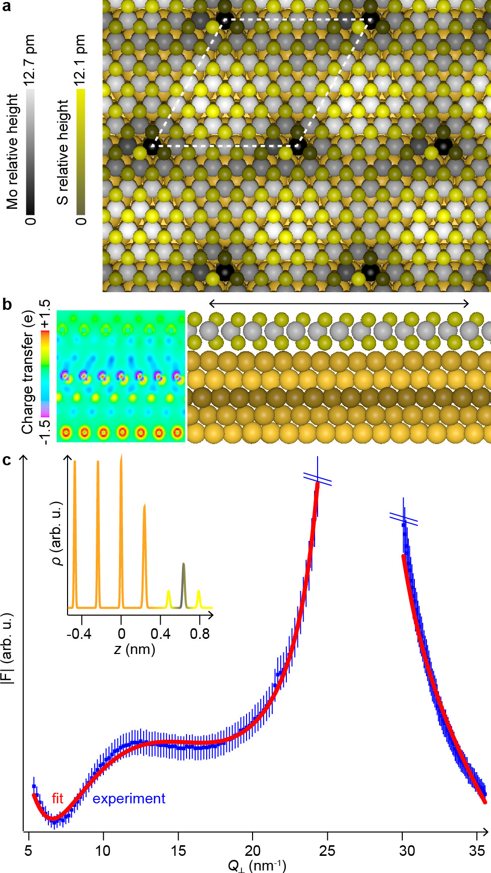
Figure 2a shows a top-view sof the minimum-energy structure of MoS2 on Au(111) that has been optimised with the DFT calculations. Periodic lattice distorsions are found in both MoS2 and Au(111). The in-plane projection of the distorsions of the topmost Au(111) layer and of the Mo layer are better visualised in Figure S2, where they have been amplified. They range from typically 1 to 8 pm (Au), and 1 to 4 pm (Mo). In another epitaxial two-dimensional material, graphene, smaller (1 pm) and larger (20 pm) distorsions have been reported on Ir(111) (Ref. 48) and Ru(0001) (Ref. 49) substrates. In the former system no or very weak moiré peaks were observed while they were clearly observed in the latter.50 Our observation of intense moiré diffraction peaks in MoS2/Au(111), and the fact that among these peaks, those located closer to the Au(111) diffraction peaks are those with higher intensity (Figure 1f), are consistent with significant distorsions in the Au lattice.
Regarding the out-of-plane structure (Figure 2b), according to the DFT calculations the average distance between the topmost Au plane and the closest S plane, , amounts 0.252 nm, while the average distance between the Mo and top (bottom) S planes is = 0.153 nm (0.156 nm). The interlayer value is smaller than the 0.312 nm interlayer distance value found in our DFT calculations for an infinite multilayer of 2H-MoS2, where the interplanar interactions are of van der Waals type. We note that the values, on the contrary, are very similar to the one obtained with multilayer of 2H-MoS2. The values of and are modulated along the moiré pattern, by only few 10 pm and few 1 pm respectively. This suggests that the apparent height modulations of typically 100 pm observed with STM in relation with the moiré pattern, are essentially of electronic nature.
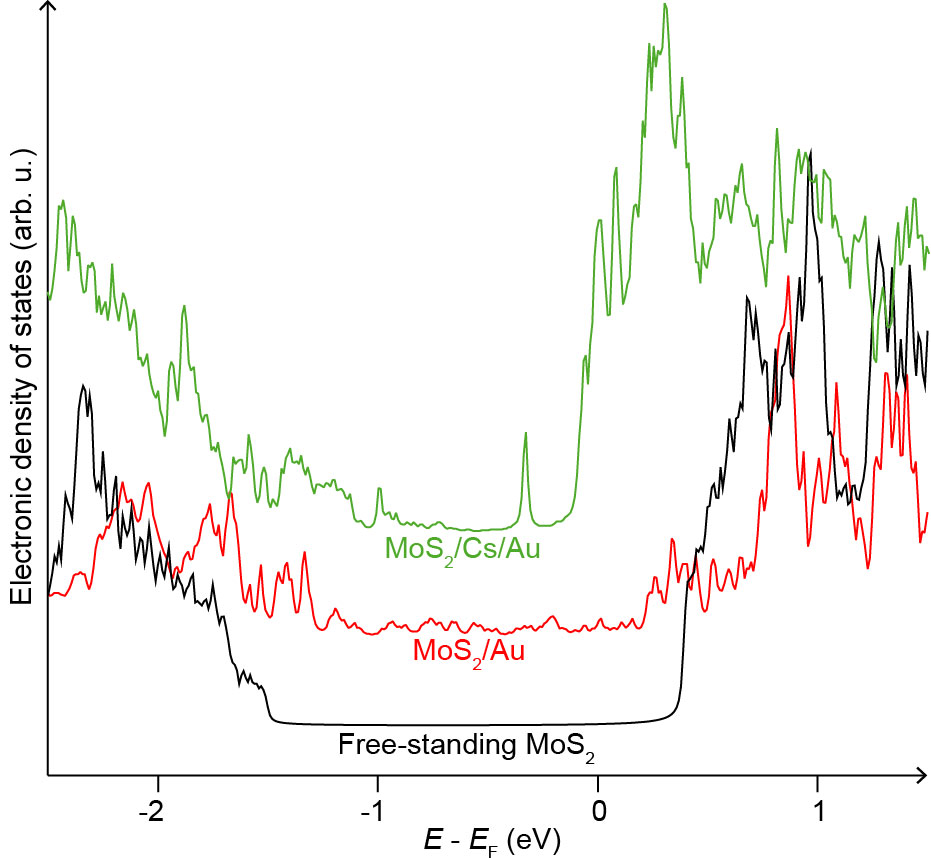
The short values shows that strong Au-S bonds exist in the system, and this is confirmed by the DFT analysis of the charge transfer at the interface between MoS2 and Au(111) (Figure 2b). Within the unit cell, a spatial modulation of the charge held by the S atoms in the bottom layer and by the Au top layers is observed. This is a signature of a spatially varying interaction between MoS2 and Au(111), which is expected when hybridization between the electronic orbitals of MoS2 and Au(111) occurs locally within the moiré, where the atoms belonging to each material are positioned properly. The bottom S layers has a deficit of electrons (blue shades in Figure 2b), while the Mo and top S layers rather have an excess of electrons (green to light-green shades in Figure 2b). This is consistent with the electronic density of states, also calculated with DFT, which shows that the bottom of the conduction band is down-shifted by about 160 meV compared to the case of free-standing MoS2 (Figure 3, see also discussion in the SI and Figure S3). Overall the DFT analysis indicates that the MoS2 single layer on Au(111) is slight electron-doped.
We now confront the DFT analysis to the experimental analysis of the out-of-plane structure via XRR. The modulus of the Fourier transform of the total electronic density of the system along the out-of-plane direction (Figure 2c) is obtained by taking the square root of the XRR data. In between the (000) and (111) crystallographic reflections of Au(111) (modulus of the out-of-plane scattering vector , 0 nm-1 and 26.68 nm-1), we observe a bump in the reflectivity. Qualitatively, the local reflectivity minima correspond to destructive interferences between the X-ray waves scattered by the Au(111) lattice and by the MoS2 layer, perpendicular to the surface. The distance between the minima is related to the distances between the layers (it decreases when the interlayer distance increases, and vice versa).
We performed a more quantitative analysis by calculating the structure factor of an atomic model of MoS2/Au(111), and refining the values of the free structural parameters to fit the calculation to the experimental data, using the ANA-ROD code.39 In short (see Figure S4a and Table S1 for details), we assume two regions that scatter incoherently, one with the bare Au(111) surface, the other with MoS2/Au(111), consistent with the partial coverage of the surface with MoS2. We disregard the above-discussed (weak) periodic distorsion, to limit the number of free parameters and thus to ensure a reliable fit. The topmost Au (111) atomic plane is let free to move in the direction, to account for surface relaxation. The above-defined and distances are also free parameters for the fit. Finally, the roughness of the surface is modeled within the so-called model,51 with as another free parameter. We obtain a very good fit to the experimental data (Figure 2c) for the electronic density profile shown in the inset of Figure 2c, that yields refined values of = 0.243 0.025 nm and = 0.153 0.022 nm. These values are in very good agreement with the outcome of the DFT calculations.
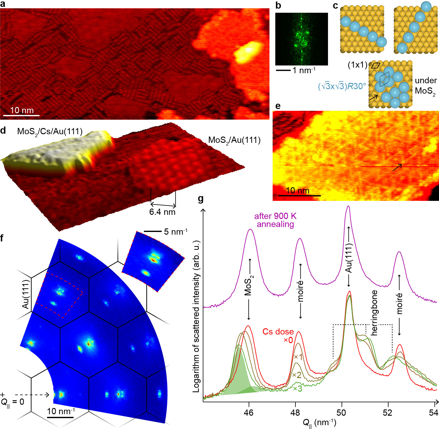
Cesium deposition and intercalation of Cs underneath MoS2. STM was performed after the nominal deposition of 0.7 Cs per Au surface atom and 500 K annealing. On MoS2-free regions Cs atoms form a pattern of 5 nm-long nanosticks, some bunching across several 1 nm to several 10 nm, and having different orientations on the surface, also detected in the Fourier transform of the images (Figure 4a,b). The strong structural disorder evident on the STM image explains the absence of a Cs-related diffraction signature at room temperature in RHEED and GIXRD. Considering the observed local periodicity, we propose two possible atomic structures for the Cs nanosticks (Figure 4c).
We observe two kinds of MoS2-covered regions (Figure 4a,d,e). Part of the MoS2 has a similar height as the Cs-covered Au(111) surface, and exhibits a moiré pattern. The majority (85%) of MoS2 islands however has a higher apparent height and exhibits no moiré pattern. A reasonable interpretation is that the latter islands are intercalated with a Cs layer, while the former islands are not. This intercalated layer is not directly accessible to STM measurements. We observe a nanoscale pattern of lines oriented along the three highest-symmetry directions of Au(111) and MoS2 (120∘ orientations). This pattern may be related to that observed in another intercalated two-dimensional-material-on-metal system, graphene/Bi/Ir(111).52 There, the pattern was interpreted as a network of dislocations in the intercalant’s lattice, the lines corresponding to the boundaries between intercalated domains being shifted by a fraction of the lattice vector(s) of the intercalant’s lattice (Figure 4c).
The disappearance of the moiré pattern observed in STM is corroborated by GIXRD measurements. After three cycles of deposition of a large Cs excess followed by 550 K annealing, the reciprocal space lattice of the sample shows no discernable moiré signals (compare Figures 4f,1e). In fact, the reduction of the moiré signals rather occurs after than before each 550 K annealing (Figure 4g). The process is hence thermally-activated, indicative of kinetically limitations.
Concomitantly to the vanishing of the moiré signal, the GIXRD data reveal that the diffraction signal associated to MoS2 progressively shows two components, the one at lower scattering vector modulus corresponding to an expansion of the lattice (Figure 4g). The latter component may be assigned to intercalated islands, while the other corresponds to pristine, still-unintercalated MoS2 islands on Au. This suggests that intercalation proceeds sequentially, island by island. In other words, the limiting kinetic step in the intercalation process corresponds to the opening of an intercalation channel, for instance a point defect or the unbinding of (part of) the flake edges from the substrate. Once this channel is opened, mass transport underneath the flake is presumably very efficient at the several-10 nm-scale considered here. At the end of the three deposition+annealing cycles, close to 100% of the islands are intercalated (note that the intensity scale in Figure 4g is logarithmic).
The GIXRD data show a decrease in intensity and an angular broadening of the diffraction peaks as the Cs dose increases (compare Figures 4f,1e), which both point to increased disorder in the form of in-plane strains and mosaic spread. Conversely, we observe a resurgence of the diffraction signals of the Au reconstruction (Figure 4g), suggesting that the Au-MoS2 interaction has been suppressed.
Strain induced by intercalation. In the absence of a significant hybridization between MoS2 and Au orbitals, the MoS2 is no more strongly pinned on the substrate lattice. Consistent with this view, the in-plane lattice parameter of MoS2 is found to change (the MoS2 diffraction peak is shifted to lower momentum transfer values, Figure 4g), i.e. the MoS2 lattice is no longer strained by its substrate. More precisely, a 0.9% lattice expansion is observed at 300 K compared to the value found in bulk MoS2.47
Several effects may explain this expansion. First, MoS2 is grown at 900 K, a temperature at which the ratio of lattice parameters for MoS2 and Au(111) is expected to be precisely 1.10,47, 53, 54 i.e. precisely the 11/10 ratio determined experimentally after the sample is cooled down to room temperature. This is yet another indication that prior to intercalation MoS2 is strongly bond on its substrate, with an epitaxial relationship that is unchanged between growth temperature and room temperature. In the opposite extreme case, if during cool down MoS2 were free to compress according to its own natural thermal compression (and not that of the Au(111) substrate, which is slightly larger), the lattice parameter of MoS2 would be slightly larger, by 0.2%.47, 53, 54 This is the maximum expansion we expect due to the suppression of the strong bonding between MoS2 and Au upon intercalation. This effect hence only accounts for a small fraction of the observed 0.9% expansion.
What is the origin of the remaining 0.7% expansion? A structural phase transition (1H to 1T or 1T’) is expected upon electron doping,55 and Cs, a well-known electro-donor species, might indeed donate the required amount of charges to MoS2. The 1T phase is not expected to have a significantly different lattice constant (a marginally shorter lattice constant has even been predicted56) while the 1T’ phase should.57 However our diffraction measurements do not detect a doubling of the MoS2 unit cell that would be expected for this phase. There is another reason why an increasing amount of alkali atoms in the vicinity of MoS2 could actually lead to an increased lattice constant. In the related system of potassium inserted in between MoS2 layers, DFT calculations predicted a significant lattice expansion. There, the role of the increased charge density within the Mo-S bonds was invoked.58 Our own DFT calculations with free-standing MoS2 (this is a rough, yet reasonable description of MoS2 decoupled from Au(111) by intercalation) predict that adding about 0.1 electrons per MoS2 unit cell (to mimik the charge transfer associated to intercalation) yields a lattice expansion by typically several 0.1%.
We again examine the structure of the sample perpendicular to the surface. While for pristine MoS2/Au(111), the XRR spectrum exhibited essentially one intensity rebound (Figure 2c), after Cs deposition and annealing at least four rebounds ( 8, 16, 22, 35 nm-1) are observed (Figure 5a). The distance between the extrema decreasing with increasing interplanar distances, this new observation is consistent with an increased distance, compared to the case of MoS2/Au(111). This is precisely what is expected if a Cs layer is intercalated between MoS2 and Au(111). To test this interpretation, we have adjusted (and the distance between the Cs layer and the Au topmost plane; see SI for further details). Given the large atomic radius of Cs, we expect a low-density Cs phase. Our STM analysis directly confirms that on MoS2-free regions (Figure 4a-c), the shortest Cs-Cs distances are indeed large, matching the second nearest neighbour Au-Au distance on the surface, i.e. 0.499 nm. Two-dimensional materials tend to alter the organisation of intercalant as shown in the case of graphene,59 hence an even lower density in the intercalated Cs layer, as e.g. in a phase, cannot be excluded a priori. However our simulations agree less with the XRR data in the case of such a low-density phase, suggesting that a denser phase, for instance a reconstruction, provides a more realistic description of the system. The best match of our model to the experimental data is obtained for = 0.551 nm and = 0.389 nm (see Table S2 for details). The value is increased by about 0.308 nm compared to the case without intercalated Cs. The increase is close, but 0.07 nm less than that observed in Cs-intercalated multilayer MoS2.60
Figure 5a obviously shows that this model is too simple to faithfully reproduce all the features in the experimental XRR data. In particular, between 15 nm-1 and 25 nm-1, the model only accounts for the baseline of the experimental spectrum, and does not produce the two marked intensity rebounds. As discussed more into details in the SI (see Figure S5 and Table S3 for another simulation with a more advanced model), what is not captured by our simple model is the multilayer thickness of the Cs layer on bare Au(111) (unlike under MoS2, where it is intercalated as a single-layer). Multilayer Cs is expected there because we chose to deposit a large excess of Cs on the surface for the samples characterized with XRR (and GIXRD), due to the lack of reliable calibration of the Cs deposition rate in the corresponding ultrahigh vacuum chamber (see Methods). On MoS2, long-ranged Cs surface diffusion and Cs desorption are instead expected already at room temperature to result in (i) low-surface-density Cs clusters, and (ii) mass transport of Cs out of the MoS2 surface, towards MoS2-free regions and vacuum. 550 K annealing will further promote this tendency, and strongly reduce the Cs cluster density on MoS2.
Thermal de-intercalation. As already mentionned, increasing the temperature promotes intercalation of Cs underneath the MoS2 flakes, which points to a kinetic barrier to intercalation (e.g. for passing through defects and/or for creating defects later acting as intercalation pathways). To further improve the efficiency of intercalation it is tempting to further increase temperature. Above about 800 K however, another key process is activated: the moiré signal re-appears in GIXRD, the MoS2 peak shifts back to its initial position (Figure 4g), and the XRR spectrum strongly resembles that of as-deposited MoS2/Au(111). In fact, after 900 K annealing, the reciprocal lattice of the sample is very similar to that of the pristine sample, i.e. Cs has been de-intercalated. How is this occurring? An XPS analysis (see SI) reveals that a fraction of Cs adatoms penetrates the Au crystal already at room temperature, even more so at 550 K (Figure S6) and at 850 K. In addition to this process, at 850 K Cs atoms may have a non-negligible probability to cross the energy barrier for diffusing outside the MoS2 islands, and to subsequently desorb to vacuum.
Electronic effects of Cs intercalation. We expect that intercalation of Cs has strong influence on the electronic properties of MoS2. We start with experimental measurements, with ARPES, of energy-momentum cuts in the electronic band structure along KKM in reciprocal space, first with the case of as-grown MoS2/Au(111). The valence band of MoS2 (whose maxima are highlighted with horizontal lines in Figure 6), with a characteristic 130 meV spin-orbit splitting at K point, is clearly seen (Figure 6a). Its maxima at and K points lie 1.67 eV and 1.35 eV respectively below the Fermi level, while the conduction band minimum is above the Fermi level, consistent with a previous report.15
After the deposition of nominally 0.3 Cs atom per surface Au atom, and thermally-induced intercalation the ARPES energy-momentum cuts (Figure 6b) and energy distribution curves (EDCs, Figure S7) show that the MoS2 valence band maximum at the and K points shift down, by 20 meV. No additional electronic band is observed that would correspond to Cs. Tripling the Cs dose yields stronger changes in the electronic band structure of MoS2 (Figures 6c,S7): the MoS2 valence band maximum at point further shifts down, by as much as 280 meV. The photoemission signal corresponding to the MoS2 valence band at the vicinity of the K point becomes weaker and broader.Inspection of the EDCs (Figure S7) is required to detect a down-shift, of about 100 meV.
The Au(111) surface state at the point, close to the Fermi level, is observed before and all along the Cs deposition/annealing procedure (Figure 6). The signature of this surface state is naturally related to the occurence of the Au(111) herringbone reconstruction observed in STM in between MoS2 islands (Figure 1c) and with GIXRD after Cs deposition/annealing (Figure 4g). This indicates that Cs is weakly adsorbed on Au, hence not altering the sensitive Au(111) reconstruction/surface state. We note that as the Cs dose increases, the surface state shifts down in binding energy (Figure 6a-c). Shifts of this kind have been observed for Na adsorbed on Cu(111),61 and have been explained by a polarization-induced filling of the surface state.62
These observations are reminiscent of a previous study that explored charge transfers induced by potassium (K) atoms in MoS2/Au(111).63 In the two studies, the most prominent effects seem to be a non-rigid down-shift of the electronic band structure, with different magnitude at and K points. The shifts are of the same order of magnitude with potassium and cesium, suggesting charge transfers (the Fermi level is changed) in the same range. The origin of the shifts can be qualitatively rationalised by inspecting the projection of the electronic states on the different orbitals in the system, which has been calculated by DFT for a (11) approximate model for MoS2 on Au(111).15 The spin-orbit-split MoS2 valence band close to K point is expected to be primarily of Mo character and the fact that it is not significantly shifted upon intercalation suggests that it is not related to a possible hybridization with the substrate’s electronic band (the hybridization would be strongly affected by intercalation), which seems reasonable for these in-plane MoS2 orbitals. In the energy range explored in Figure 6, at point the stronger contribution to the valence band stems from Mo out-of-plane orbitals, and these bands are indeed expected to be involved in the hybridization and charge transfers with the substrate or the alkali atoms, consistent with our observations (Figure 6).
The broadening of the valence band at K point after Cs intercalation points to a significant disorder in the system. This is consistent with our STM observations of a disordered nanoscaled pattern for Cs in this case (Figure 4c,e). Strikingly, annealing the sample to 850 K allows to recover a well-defined valence band at K point (compare Figure 6a,d), consistent with the deintercalation process also evident in GIXRD (Figure 4g) and XRR, which we interpret as a consequence of Cs diffusion into bulk Au or Cs desorption from the surface. This is also an indication that the source of electronic disorder was indeed extrinsic to the MoS2, i.e. due to the intercalant, and not intrinsic to MoS2, i.e. due to the creation of defects in the dichalcogenide single-layer.
Our ARPES observation can be rationalised in the framework of a simplified DFT calculation scheme. Minimising the structure of the MoS2/Cs/Au(111) system would require to consider a large commensurate calculation supercell comprising about 1,100 atoms (in a , and not a (11), moiré unit cell), among which high- number ones. This is computationally prohibitive, and we prefer, instead, to analyse the electronic density of states for the values of = 0.389 nm and = 0.551 nm (see structural model represented in Figures 5b,c) which we derived from the analysis of the XRR data. Keeping in mind the limitations of the latter analysis, we also considered another set of and values, for which the Cs layer is further from (closer to) the MoS2 layer (Au(111) surface), see SI for details.
Figure 3 compares the electronic density of states in the presence of the intercalated layer ( = 0.389 nm, = 0.551 nm) to the case of MoS/Au(111) and the case of isolated MoS2. The bottom of the conduction band is further down-shifted, by about 320 meV, relative to the case of MoS2/Au(111), which is indicative of a strong electron doping of MoS2, consistent with our ARPES observations. This tendency is robust and is also predicted for different and values (Figure S3). The level of electronic doping seems comparable to the one that we expect for an isolated MoS2 layer, with three Cs atoms adsorbed per MoS2 unit cells (Figure S3).
Except for one marked peak (-330 meV) that we ascribe to an interfacial Au/Cs state, within about 600 meV below the bottom of the conduction band, the DFT calculations predict few in-gap states than for MoS2/Au(111). Below this energy range more in-gap states are predicted, at least for = 0.389 nm and = 0.551 nm. Their occurrence is however highly dependent on the distance between the bottom S layer and the Cs layer, as shown for a calculation performed with another set of and values (Figure S3).
4 Conclusions
We showed that starting from MoS2 flakes strongly coupled to the Au(111) substrate, with a short spacing and a substantial nanorippling, Cs intercalation lifts the flakes and flatens them. The process is thermally activated. De-intercalation is also thermally activated, but at higher temperatures. We found that Cs, which is intercalated in the form of a atomic layer whose density is consistent with a reconstruction on Au(111), substantially dopes MoS2 with electrons, and that this doping is a possible origin for a 1% expansion of the atomic lattice of MoS2 parallel to the surface. The interaction with the Cs layer is associated with relative changes in the energy of the valence band maxima and to electronic disorder presumably related to the structural disorder in Cs.
Our work opens new perspectives towards the manipulation of two-dimensional transition metal dichalcogenides. Similarly to in-solution strategies,29 intercalation could be exploited on MoS2/Au(111) to facilitate the exfoliation of nanoscale flakes12 or full layers.14 Demonstrating further control on electronic or hole doping of MoS2 with intercalated electro-donor or electro-acceptor species is another exciting goal. A number of species, to be intercalated with varying doses, are relevant here, among the vast catalog of alkali atoms, transition metals, and molecules. Finally, as extensively demonstrated with bulk compounds in the past, intercalation opens new doors to achieve a variety of two-dimensional phases, structural ones, magnetic ones, and even superconducting ones.
R.S. acknowledges financial support by Nanosciences Foundation. This work was supported by the 2DTransformers project under the OH-RISQUE program (ANR-14-OHRI-0004), J2D (ANR-15-CE24-0017) and ORGANI’SO (ANR-15-CE09-0017) projects of Agence Nationale de la Recherche (ANR), by the French state funds Equipex ANR-11-EQPX-0010, ANR-10-LABX-51-01 (Labex LANEF of "Programme d’Investissements d’Avenir"), ANR-15-IDEX-02, and by the Région Rhône Alpes (ARC6 program) and the Labex LANEF. The was also supported by VILLUM FONDEN via the Centre of Excellence for Dirac Materials (Grant No. 11744). We thank Tao Zhou for his kind support.
Supporting information comprises additional STM data showing defects in MoS2, the results of DFT calculations on deformations in MoS2 and its substrate, energy distribution ARPES curves, and a DFT analysis of the the influence of an intercalated AuCs alloy on the electronic properties of MoS2.
References
- Splendiani et al. 2010 Splendiani, A.; Sun, L.; Zhang, Y.; Li, T.; Kim, J.; Chim, C.-Y.; Galli, G.; Wang, F. Emerging Photoluminescence in Monolayer MoS2. Nano Lett. 2010, 10, 1271–1275
- Mak et al. 2010 Mak, K. F.; Lee, C.; Hone, J.; Shan, J.; Heinz, T. F. Atomically Thin MoS2: A New Direct-Gap Semiconductor. Phys. Rev. Lett. 2010, 105, 136805
- Radisavljevic et al. 2011 Radisavljevic, B.; Radenovic, A.; Brivio, J.; Giacometti, i. V.; Kis, A. Single-Layer MoS2 Transistors. Nat. Nanotech. 2011, 6, 147
- Zhan et al. 2012 Zhan, Y.; Liu, Z.; Najmaei, S.; Ajayan, P. M.; Lou, J. Large-Area Vapor-Phase Growth and Characterization of MoS2 Atomic Layers on a SiO2 Substrate. Small 2012, 8, 966–971
- Liu et al. 2012 Liu, K.-K.; Zhang, W.; Lee, Y.-H.; Lin, Y.-C.; Chang, M.-T.; Su, C.-Y.; Chang, C.-S.; Li, H.; Shi, Y.; Zhang, H. et al. Growth of Large-Area and Highly Crystalline MoS2 Thin Layers on Insulating substrates. Nano Lett. 2012, 12, 1538–1544
- Lee et al. 2012 Lee, Y.-H.; Zhang, X.-Q.; Zhang, W.; Chang, M.-T.; Lin, C.-T.; Chang, K.-D.; Yu, Y.-C.; Wang, J. T.-W.; Chang, C.-S.; Li, L.-J. et al. Synthesis of Large-Area MoS2 Atomic Layers with Chemical Vapor Deposition. Adv. Mater. 2012, 24, 2320–2325
- Eichfeld et al. 2015 Eichfeld, S. M.; Hossain, L.; Lin, Y.-C.; Piasecki, A. F.; Kupp, B.; Birdwell, A. G.; Burke, R. A.; Lu, N.; Peng, X.; Li, J. et al. Highly Scalable, Atomically Thin WSe2 Grown via Metal-Organic Chemical Vapor Deposition. ACS Nano 2015, 9, 2080–2087
- Kim et al. 2011 Kim, D.; Sun, D.; Lu, W.; Cheng, Z.; Zhu, Y.; Le, D.; Rahman, T. S.; Bartels, L. Toward the Growth of an Aligned Single-Layer MoS2 Film. Langmuir 2011, 27, 11650–11653
- Orofeo et al. 2014 Orofeo, C. M.; Suzuki, S.; Sekine, Y.; Hibino, H. Scalable Synthesis of Layer-Controlled WS2 and MoS2 Sheets by Sulfurization of Thin Metal Films. Appl. Phys. Lett. 2014, 105, 083112
- Wang et al. 2015 Wang, Y.; Li, L.; Yao, W.; Song, S.; Sun, J.; Pan, J.; Ren, X.; Li, C.; Okunishi, E.; Wang, Y.-Q. et al. Monolayer PtSe2, a New Semiconducting Transition-Metal-Dichalcogenide, Epitaxially Grown by Direct Selenization of Pt. Nano Lett. 2015, 15, 4013–4018
- Ugeda et al. 2014 Ugeda, M. M.; Bradley, A. J.; Shi, S.-F.; Felipe, H.; Zhang, Y.; Qiu, D. Y.; Ruan, W.; Mo, S.-K.; Hussain, Z.; Shen, Z.-X. et al. Giant Bandgap Renormalization and Excitonic Effects in a Monolayer Transition Metal Dichalcogenide Semiconductor. Nat. Mater. 2014, 13, 1091–1095
- Helveg et al. 2000 Helveg, S.; Lauritsen, J. V.; Lægsgaard, E.; Stensgaard, I.; Nørskov, J. K.; Clausen, B.; Topsøe, H.; Besenbacher, F. Atomic-Scale Structure of Single-Layer MoS2 Nanoclusters. Phys. Rev. Lett. 2000, 84, 951
- Sørensen et al. 2014 Sørensen, S. G.; Füchtbauer, H. G.; Tuxen, A. K.; Walton, A. S.; Lauritsen, J. V. Structure and Electronic Properties of In Situ Synthesized Single-Layer MoS2 on a Gold Surface. ACS Nano 2014, 8, 6788–6796
- Bana et al. 2018 Bana, H.; Travaglia, E.; Bignardi, L.; Lacovig, P.; Sanders, C. E.; Dendzik, M.; Michiardi, M.; Bianchi, M.; Lizzit, D.; Presel, F. et al. Epitaxial Growth of Single-Orientation High-Quality MoS2 Monolayers. 2D Mater. 2018, 5, 035012
- Bruix et al. 2016 Bruix, A.; Miwa, J. A.; Hauptmann, N.; Wegner, D.; Ulstrup, S.; Grønborg, S. S.; Sanders, C. E.; Dendzik, M.; Čabo, A. G.; Bianchi, M. et al. Single-Layer MoS2 on Au(111): Band Gap Renormalization and Substrate Interaction. Phys. Rev. B 2016, 93, 165422
- Krane et al. 2018 Krane, N.; Lotze, C.; Franke, K. J. Moiré Structure of MoS2 on Au(111): Local Structural and Electronic Properties. Surf. Sci. 2018, 678, 136–142
- Krane et al. 2016 Krane, N.; Lotze, C.; Läger, J. M.; Reecht, G.; Franke, K. J. Electronic Structure and Luminescence of Quasi-Freestanding MoS2 Nanopatches on Au(111). Nano Lett. 2016, 16, 5163–5168
- Varykhalov et al. 2008 Varykhalov, A.; Sánchez-Barriga, J.; Shikin, A.; Biswas, C.; Vescovo, E.; Rybkin, A.; Marchenko, D.; Rader, O. Electronic and Magnetic Properties of Quasifreestanding Graphene on Ni. Phys. Rev. Lett. 2008, 101, 157601
- Riedl et al. 2009 Riedl, C.; Coletti, C.; Iwasaki, T.; Zakharov, A.; Starke, U. Quasi-Free-Standing Epitaxial Graphene on SiC Obtained by Hydrogen Intercalation. Phys. Rev. Lett. 2009, 103, 246804
- Mahatha et al. 2018 Mahatha, S. K.; Dendzik, M.; Sanders, C. E.; Michiardi, M.; Bianchi, M.; Miwa, J. A.; Hofmann, P. Quasi-Free-Standing Single-Layer WS2 Achieved by Intercalation. Phys. Rev. Materials 2018, 2, 124001
- Friend and Yoffe 1987 Friend, R.; Yoffe, A. Electronic Properties of Intercalation Complexes of the Transition Metal Dichalcogenides. Adv. Phys. 1987, 36, 1–94
- Murugan et al. 2006 Murugan, A. V.; Quintin, M.; Delville, M.-H.; Campet, G.; Gopinath, C. S.; Vijayamohanan, K. Exfoliation-Induced Nanoribbon Formation of Poly(3,4-Ethylene Dioxythiophene) PEDOT Between MoS2 Layers as Cathode Material for Lithium Batteries. J. Power Sources 2006, 156, 615–619
- Whittingham 1976 Whittingham, M. S. Electrical Energy Storage and Intercalation Chemistry. Science 1976, 192, 1126–1127
- Feng et al. 2009 Feng, C.; Ma, J.; Li, H.; Zeng, R.; Guo, Z.; Liu, H. Synthesis of Molybdenum Disulfide (MoS2) for Lithium Ion Battery Applications. Mater. Res. Bull. 2009, 44, 1811–1815
- Li et al. 2019 Li, Z.; Jiang, K.; Khan, F.; Goswami, A.; Liu, J.; Passian, A.; Thundat, T. Anomalous Interfacial Stress Generation During Sodium Intercalation/Extraction in MoS2 Thin-Film Anodes. Sci. Adv. 2019, 5, eaav2820
- Py and Haering 1983 Py, M.; Haering, R. Structural Destabilization Induced by Lithium Intercalation in MoS2 and Related Compounds. Canadian J. Phys. 1983, 61, 76–84
- Wypych and Schöllhorn 1992 Wypych, F.; Schöllhorn, R. 1T-MoS2, a New Metallic Modification of Molybdenum Disulfide. J. Chem. Soc. Chem. Comm. 1992, 1386–1388
- Heising and Kanatzidis 1999 Heising, J.; Kanatzidis, M. G. Structure of Restacked MoS2 and WS2 Elucidated by Electron Crystallography. J. Am. Chem. Soc. 1999, 121, 638–643
- Eda et al. 2011 Eda, G.; Yamaguchi, H.; Voiry, D.; Fujita, T.; Chen, M.; Chhowalla, M. Photoluminescence from Chemically Exfoliated MoS2. Nano Lett. 2011, 11, 5111–5116
- Wang et al. 2013 Wang, Y.; Ou, J. Z.; Balendhran, S.; Chrimes, A. F.; Mortazavi, M.; Yao, D. D.; Field, M. R.; Latham, K.; Bansal, V.; Friend, J. R. et al. Electrochemical Control of Photoluminescence in Two-Dimensional MoS2 Nanoflakes. ACS Nano 2013, 7, 10083–10093
- Wang et al. 2014 Wang, X.; Shen, X.; Wang, Z.; Yu, R.; Chen, L. Atomic-Scale Clarification of Structural Transition of MoS2 Upon Sodium Intercalation. ACS Nano 2014, 8, 11394–11400
- Fan et al. 2015 Fan, X.; Xu, P.; Zhou, D.; Sun, Y.; Li, Y. C.; Nguyen, M. A. T.; Terrones, M.; Mallouk, T. E. Fast and Efficient Preparation of Exfoliated 2H-MoS2 Nanosheets by Sonication-Assisted Lithium Intercalation and Infrared Laser-Induced 1T to 2H Phase Reversion. Nano Lett. 2015, 15, 5956–5960
- Guo et al. 2015 Guo, Y.; Sun, D.; Ouyang, B.; Raja, A.; Song, J.; Heinz, T. F.; Brus, L. E. Probing the Dynamics of the Metallic-to-Semiconducting Structural Phase Transformation in MoS2 Crystals. Nano Lett. 2015, 15, 5081–5088
- Xiong et al. 2015 Xiong, F.; Wang, H.; Liu, X.; Sun, J.; Brongersma, M.; Pop, E.; Cui, Y. Li Intercalation in MoS2: In Situ Observation of its Dynamics and Tuning Optical and Electrical Properties. Nano Lett. 2015, 15, 6777–6784
- Ahmad et al. 2017 Ahmad, M.; Müller, E.; Habenicht, C.; Schuster, R.; Knupfer, M.; Büchner, B. Semiconductor-to-Metal Transition in the Bulk of WSe2 Upon Potassium Intercalation. J Physics: Condens. Matter. 2017, 29, 165502
- Hoffmann et al. 2004 Hoffmann, S.; Søndergaard, C.; Schultz, C.; Li, Z.; Hofmann, P. An Undulator-Based Spherical Grating Monochromator Beamline for Angle-Resolved Photoemission Spectroscopy. Nucl. Instrum. Methods Phys. Res. Sect. A 2004, 523, 441–453
- Taborek and Rutledge 1992 Taborek, P.; Rutledge, J. Novel Wetting Behavior of 4He on Cesium. Phys. Rev. Lett. 1992, 68, 2184
- Petrović et al. 2013 Petrović, M.; Rakić, I. Š.; Runte, S.; Busse, C.; Sadowski, J.; Lazić, P.; Pletikosić, I.; Pan, Z.-H.; Milun, M.; Pervan, P. et al. The Mechanism of Caesium Intercalation of Graphene. Nat. Commun. 2013, 4, 1–8
- Vlieg 2000 Vlieg, E. ROD: a Program for Surface X-Ray Crystallography. J. Appl. Cryst. 2000, 33, 401–405
- Lewis et al. 2011 Lewis, J. P.; Jelínek, P.; Ortega, J.; Demkov, A. A.; Trabada, D. G.; Haycock, B.; Wang, H.; Adams, G.; Tomfohr, J. K.; Abad, E. et al. Advances and Applications in the FIREBALL Ab Initio Tight-Binding Molecular-Dynamics Formalism. Phys. Stat. Sol. b 2011, 248, 1989–2007
- Jelínek et al. 2005 Jelínek, P.; Wang, H.; Lewis, J. P.; Sankey, O. F.; Ortega, J. Multicenter Approach to the Exchange-Correlation Interactions in Ab Initio Tight-Binding Methods. Phys. Rev. B 2005, 71, 235101
- Sankey and Niklewski 1989 Sankey, O. F.; Niklewski, D. J. Ab Initio Multicenter Tight-Binding Model for Molecular-Dynamics Simulations and Other Applications in Covalent Systems. Phys. Rev. B 1989, 40, 3979
- González et al. 2016 González, C.; Biel, B.; Dappe, Y. J. Theoretical Characterisation of Point Defects on a MoS2 Monolayer by Scanning Tunnelling Microscopy. Nanotechnology 2016, 27, 105702
- Grønborg et al. 2015 Grønborg, S. S.; Ulstrup, S.; Bianchi, M.; Dendzik, M.; Sanders, C. E.; Lauritsen, J. V.; Hofmann, P.; Miwa, J. A. Synthesis of Epitaxial Single-Layer MoS2 on Au(111). Langmuir 2015, 31, 9700–9706
- Bollinger et al. 2001 Bollinger, M.; Lauritsen, J.; Jacobsen, K. W.; Nørskov, J. K.; Helveg, S.; Besenbacher, F. One-Dimensional Metallic Edge States in MoS2. Phys. Rev. Lett. 2001, 87, 196803
- Guinier 1994 Guinier, A. X-ray diffraction in crystals, imperfect crystals, and amorphous bodies; Dover Publications, 1994
- El-Mahalawy and Evans 1976 El-Mahalawy, S.; Evans, B. The Thermal Expansion of 2H-MoS2, 2H-MoSe2 and 2H-WSe2 between 20 and 800∘C. J. Appl. Cryst. 1976, 9, 403–406
- Blanc et al. 2012 Blanc, N.; Coraux, J.; Vo-Van, C.; N’Diaye, A. T.; Geaymond, O.; Renaud, G. Local Deformations and Incommensurability of High-Quality Epitaxial Graphene on a Weakly Interacting Transition Metal. Phys. Rev. B 2012, 86, 235439
- Martoccia et al. 2010 Martoccia, D.; Björck, M.; Schlepütz, C.; Brugger, T.; Pauli, S.; Patterson, B.; Greber, T.; Willmott, P. Graphene on Ru(0001): a Corrugated and Chiral Structure. New J. Phys. 2010, 12, 043028
- Martoccia et al. 2008 Martoccia, D.; Willmott, P.; Brugger, T.; Björck, M.; Günther, S.; Schlepütz, C.; Cervellino, A.; Pauli, S.; Patterson, B.; Marchini, S. et al. Graphene on Ru (0001): a 25 25 Supercell. Phys. Rev. Lett. 2008, 101, 126102
- Robinson 1986 Robinson, I. K. Crystal Truncation Rods and Surface Roughness. Phys. Rev. B 1986, 33, 3830
- Warmuth et al. 2016 Warmuth, J.; Bruix, A.; Michiardi, M.; Hänke, T.; Bianchi, M.; Wiebe, J.; Wiesendanger, R.; Hammer, B.; Hofmann, P.; Khajetoorians, A. A. Band-Gap Engineering by Bi Intercalation of Graphene on Ir(111). Phys. Rev. B 2016, 93, 165437
- Huang et al. 2014 Huang, L. F.; Gong, P. L.; Zeng, Z. Correlation between Structure, Phonon Spectra, Thermal Expansion, and Thermomechanics of Single-Layer MoS2. Phys. Rev. B 2014, 90, 045409
- Nix and MacNair 1941 Nix, F.; MacNair, D. The Thermal Expansion of Pure Metals: Copper, Gold, Aluminum, Nickel, and Iron. Phys. Rev. 1941, 60, 597
- Brumme et al. 2015 Brumme, T.; Calandra, M.; Mauri, F. First-Principles Theory of Field-Effect Doping in Transition-Metal Dichalcogenides: Structural Properties, Electronic Structure, Hall Coefficient, and Electrical Conductivity. Phys. Rev. B 2015, 91, 155436
- Duerloo et al. 2014 Duerloo, K.-A. N.; Li, Y.; Reed, E. J. Structural Phase Transitions in Two-Dimensional Mo-and W-Dichalcogenide Monolayers. Nat. Commun. 2014, 5, 4214
- Tan et al. 2018 Tan, S. J. R.; Sarkar, S.; Zhao, X.; Luo, X.; Luo, Y. Z.; Poh, S. M.; Abdelwahab, I.; Zhou, W.; Venkatesan, T.; Chen, W. et al. Temperature- and Phase-Dependent Phonon Renormalization in 1T’-MoS2. ACS Nano 2018, 12, 5051–5058
- Andersen et al. 2012 Andersen, A.; Kathmann, S. M.; Lilga, M. A.; Albrecht, K. O.; Hallen, R. T.; Mei, D. First-Principles Characterization of Potassium Intercalation in Hexagonal 2H-MoS2. J. Phys. Chem. C 2012, 116, 1826–1832
- Martínez-Galera et al. 2016 Martínez-Galera, A. J.; Schröder, U.; Huttmann, F.; Jolie, W.; Craes, F.; Busse, C.; Caciuc, V.; Atodiresei, N.; Blügel, S.; Michely, T. Oxygen Orders Differently Under Graphene: New Superstructures on Ir (111). Nanoscale 2016, 8, 1932–1943
- Somoano et al. 1973 Somoano, R.; Hadek, V.; Rembaum, A. Alkali Metal Intercalates of Molybdenum Disulfide. J. Chem. Phys. 1973, 58, 697–701
- Lindgren and Walldén 1980 Lindgren, S.; Walldén, L. Photoemission of Electrons at the Cu(111)/Na Interface. Solid State Commun. 1980, 34, 671–673
- Forster et al. 2006 Forster, F.; Bendounan, A.; Ziroff, J.; Reinert, F. Systematic Studies on Surface Modifications by ARUPS on Shockley-Type Surface States. Surf. Sci. 2006, 600, 3870–3874
- Miwa et al. 2015 Miwa, J. A.; Ulstrup, S.; Sørensen, S. G.; Dendzik, M.; Čabo, A. G.; Bianchi, M.; Lauritsen, J. V.; Hofmann, P. Electronic Structure of Epitaxial Single-Layer MoS2. Phys. Rev. Lett. 2015, 114, 046802