Supporting Informations: Compact SQUID realized in a double layer graphene heterostructure
keywords:
Supporting Informations: Double layer graphene, SQUID, van der Waals heterostructure, helical states, supercurrent LaTeXSwiss Nanoscience institute, University of Basel, Klingelbergstrasse 82, CH-4056 Basel, Switzerland \alsoaffiliationSwiss Nanoscience institute, University of Basel, Klingelbergstrasse 82, CH-4056 Basel, Switzerland
0.1 Device fabrication
The fabrication of the van der Waals heterostructure (vdWh), superconducting contacts, and gates is described in the following section. In a first step all the 2D materials, i.e. graphite and hBN, were exfoliated on a silicon wafer with an oxide thickness of 295 nm using the low adhesion tape ELP BT-150P-LC supplied by Nitto. We identified the graphene by the optical contrast difference of 4 in the green channel with respect to the substrate 1. The thickness of the middle hBN and its plateaus were measured by an atomic force microscope (AFM) using a Bruker Dimension 3100 in tapping mode at ambient conditions.
The stacking of the different crystals was done by a well established technique, which uses a polycarbonate (PC) film on a polydimethylsiloxane (PDMS) pillow 2. Here, the such fabricated vdWh consists from bottom to top out of thick graphite, a bottom hBN, a bottom graphene, a middle hBN, a top graphene, and a top hBN flake. Important to mention is that only the top surface of the top hBN flake is in contact with the PC, such that the entire stacking process is fully assisted by the van der Waals forces and it can be considered dry and polymer free. Further the encapsulation protects the graphene layers from contaminations during the device fabrication. In the end the stack was placed at 170 ∘C on a intrinsic silicon wafer with an oxide thickness of 285 nm. At these temperature the PC detaches fully from the PDMS pillow. The PC residues on top of the stack can be dissolved in dichlormethane for 1 h at room temperature. To clean the top hBN’s surface, the stack was annealed at a temperature of 300 ∘C for 3 h in forming gas (H2 8/N2 92) at a background pressure of 20 mbar. This removes remaining PC residues.
During the stacking process it is possible that impurities are trapped between two layers, which manifest themselves in the appearance of bubbles. Using an AFM we can map the clean areas, i.e. the areas without bubbles, which are used for the device fabrication. Further we can determine the thickness of the different hBN, which is important to determine the exact etching times and for the calculation of the electrostatics.
The two layers of graphene have been connected by several common superconducting edge contacts forming several Josephson junctions (JJs) in series. To fabricate the contacts we used standard electron beam lithography (EBL). A e-beam resist of PMMA 950k, which is dissolved in anisole (concentration of 5.5), was spin coated with 4000 rpm for 40 s on the sample, resulting in a film thickness of 380 nm. The EBL was performed with an acceleration voltage of 20 kV and a dose of 400 C/cm2. The resist was developed for 1 min in a IPA/deionized water mixture (7/3) cooled to 5∘C and was then blow dried with nitrogen. To fabricate the superconducting edge contacts the stack was etched by a reactive ion etching using a CHF3/O2 plasma with 40 sccm/4 sccm at a background pressure of 60 mTorr and a power of 60 W. The rate of the etching recipe was calibrated in advance to have a very precise control of the amount of etched hBN. This is crucial, since one has to stop the etching process in the bottom hBN layer, such that the bottom gate is electrically insulated from the MoRe electrodes, but both graphene layers can be contacted simultaneously. After the etching, the MoRe was sputtered in a AJA ATC Orion using still the same PMMA mask. For the sputtering we used a target of Mo/Re 1:1, a power of 100 W, a background pressure of 2 mTorr, and a constant Argon flow of 30 sccm. The contacts have a thickness of 80 nm. The lift-off was done in acetone at 50 ∘C. In a next step the MoRe was contacted by Cr/Au (5 nm/125 nm) using another EBL defined mask and electron beam evaporation at a pressure of 5e-7mbar. After the lift-off, an etching mask was prepared by EBL to shape the mesa. To insulate the structure from the topgate it was overgrown by an uniform Al2O3 layer of 30 nm using atomic layer deposition (ALD), which involved trimethylaluminium (TMA) and water. We observed that for a homogeneous growth of the Al2O3 on the vdWh a short O2 plasma (flow 16 sccm, pressure 250 mTorr, power 30 W, time 20 s) is needed. This removes remaining polymer residues from the fabrication and leads to a homogeneous wetting of the surfaces. In last step we deposited the metallic topgate.
0.2 Normal state resitance
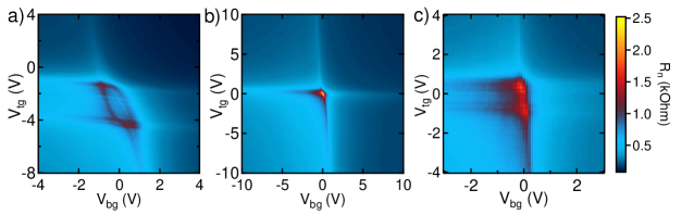
The normal state resistance () was measured for three different junctions with different inter layer distances () by applying a bias voltage of 4 mV, which is larger then twice meV 3. For the junctions with =12 nm and 50 nm we observed two Dirac points (DP) as a function of the top gate voltage () (see Fig.S1 a and c). We attribute this behavior to a inhomogeneous lateral residual doping in the top graphene layer. The splitting of the DP as a function of the back gate voltage () around charge neutrality (see Fig.S1 a) can then be explained by the density of states (DOS) dependent screening of the top gate by the different top graphene regions. For the junction with a thickness of 25 nm, this behavior is less pronounced, but the DP of the top graphene is broadened in charge carrier density compared to the bottom one, which can may be attributed to the same effect.
The Fabry-Pérot cavity length (), i.e. the size of the p doped region, at large and is extracted from the location of neighbouring resistance maxima in charge carrier density using Eq.1 4.
| (1) |
where is the position in carrier density of the i-th peak in resistance. We obtain a length of around 550 nm. The comparison to =650 nm of J2 indicates that the n doped region at each contact is of the order of 50 nm for large densities.
To extract the mobility and contact resistance of J2 we fit the conductivities, which are plotted in the article in Fig.1 d, by:
| (2) |
where is the residual conductivity at the DP, and is the contact resistivity. From the fit we obtain an electron mobility of around 53’000 cm2/Vs (33’000 cm2/Vs) and a hole mobility of around 27’000 cm2/Vs (14’000 cm2/Vs) for the bottom (top) graphene. An of 170 (190 ) and 440 (490 ) is extracted for the bottom (top) graphene for the n-doping and the p-doping, respectively.
0.3 Electrostatic model
The charge carrier density in the top () and the bottom () graphene were calculated from and using the electrostatic model described in the following section. The structure, which we consider is a DLG (see Fig.S2), consisting of the following layers listed from bottom to top: 1) graphite bottom gate 2) bottom hBN 3) bottom graphene layer 4) middle hBN 5) top graphene layer 6) top hBN 7) aluminium oxide 8) metal top gate.
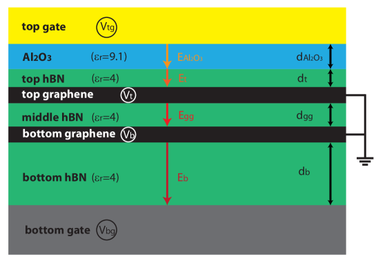
The top gate is electrically separated from the top graphene by an aluminium oxide layer with a thickness of and a dielectric constant and the top hBN with a thickness of and . A hBN with a thickness of between the two graphene sheets electrically disconnects the two layers, which are shorted at two common 1D edge contacts. hBN was also used as a dielectric material between the bottom graphene plus electrodes and the bottom gate. The thickness of the bottom hBN layer is given by . Since the two graphene layers are electrically shorted, they are at the same electro-chemical potential, which is chosen to be equal to zero, i.e. ground, for the following calculation. From this follows that,
| (3) |
where , are the chemical potential and , are the electrostatic potential of the top, respectively the bottom graphene and is the elementary charge. For graphene the chemical potential is given as,
| (4) |
where the charge carrier density in the -th graphene layer. The function is such that it is positive for electron doped and negative for hole doped graphene.
To describe the electrostatic situation we look carefully at the electric fields , where the index denotes the different dielectrics, which are a consequence of applied gate voltages, quantum capacitance and charge carrier density on either graphene. The electric fields are defined as shown in Fig.S2. In a first step we express in terms of . If we consider the interface between the two dielectric materials to be charge free, it follows directly from the Maxwell equations that normal components of the two electric fields times their dielectric constant have to be the same at the interface. In this case is given by,
| (5) |
Using Gauss law we can write down and as a function of the electric fields.
| (6) |
| (7) |
where the vacuum permittivity is given as . Further the electric fields are given by the voltage differences between the layers and leads to the following sets of equations:
| (8) |
| (9) |
| (10) |
| (11) |
From Eq.8 we obtain that , while can be expressed as a function of and using Eq.7. Therefore it follows that is given as,
| (12) |
The same can be done for starting from Eq.10. By using the relation between the two electric fields one obtains that,
| (13) |
For simplification we define . Again we can replace with Eq.6 and in the and we obtain the result,
| (14) |
Measurement of
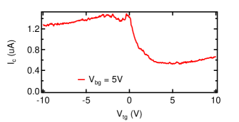
was measured using a FCA3000 counter. The appearance of a finite voltage () over the junction was triggered, while sweeping the bias current. The value of was set to 6V to be able to measure in the entire gate range, e.g. small at the DP, since the smallest detectable value is given by nA. This small trigger voltage makes the measurement sensitive to voltage noise, which can lead to a trigger error and results in a reduced value for . Due to this, the maximum value of hundred measurements of the stochastic switching current is taken, which deviates not more then 10 from the mean value, since the mean value also contains the trigger errors.
of
The product of and in a JJ in the long regime, namely that the junction length is larger than the superconducting coherence length (), is proportional to the Thouless energy () 5, 6. This energy is inversely proportional to the time () that a charge carrier spends in the junction, i.e. the graphene. For a ballistic junction , where the junction length.
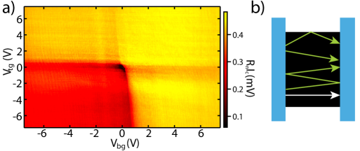
for J2 is shown in Fig.S3 a. We observe a constant value in each quadrant apart the DPs, i.e. nn, np, pn, and pp, for the product, which indicates a constant value of . Nevertheless, the value never reaches the expected one of 1 mV given by m/s for graphene and the junction length nm. This points into the direction, that the superconducting path decohere stronger than expected. Further, varies between the different quadrants. While it is equal to 0.4 mV, if both layers are n doped, it decreases to 0.25 mV in the pp regime. This points into the direction that the imperfect contacts are leading to a suppression of . This can be seen as the charge carrier are spending an effectively longer time than in the junction, which can be due to reflection at the contacts or the physical graphene edges (see Fig.S3 b).
Suppressed resistance in moderate out-of-plane magnetic fields
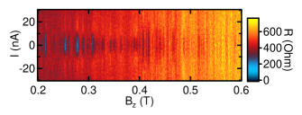
At magnetic fields large enough to suppress the supercurrent in the JJ but smaller than the field needed to be in the quantum Hall (QH) regime, irregular oscillations of the resistance around zero dc-current bias are observed (see Fig.S4). The gate voltages were set to =-1.5 V and =1.5 V, while the resistance as a function of out-of-plane magnetic field () was measured with a standard lockin technique. The ac-current amplitude was set to 50 pA. The appearance of these random oscillations were already observed by Ben Shalom et al.7 and are attributed to the ballistic transport nature of the junction, which leads to billiard like trajectories at the edges of the sample. These trajectories are suspected to form irregularly Andreev states, while the ones in the bulk are fully suppressed by the magnetic field. Therefore, it is another indication of the ballistic transport nature of J2. Nevertheless, the observation of this superconducting pockets disappears at fields larger than 440 mT and were not observed in the QH regime within our resolution of 50 pA as shown in Ref.8.
Calibration and alignment of the in-plane magnetic field
To measure the in-plane magnetic field dependence of such a DLG SQUID device, one has to carefully calibrate and adjust the direction of the magnetic field. Due to the large ratio between the JJs area and the area of the SQUID loop, e.g. 1:35 for J2, the of each JJ is more sensitive to an out-of-plane magnetic field than of the SQUID to an in-plane field. If the alignment is imperfect, which results in a finite out-of-plane component, the SQUID interference pattern decays due to the interference of the supercurrent in the individual junctions. Further we will show that also a component x-direction (see Fig.S5 c) leads to a reduction in as well.
The calibration was performed using a 3D vector magnet with the magnetic fields , , and , which are perpendicular to each other. While the graphene plane was roughly lying in the plane of the first and second magnet with and , the magnetic field of the third one is pointing out-of-plane. In a first step we had to measure three different points, which are in the xy-plane of the sample. This was done by setting the values of the first and second magnet to the values given in the inset of Fig.S5 a. At each point the out-of-plane magnetic field () was swept and a Fraunhofer like interference pattern was measured. The point in , where is maximal reflects the best compensation of the out-of-plane magnetic field, i.e. correspond to a magnetic field in the plane of the JJs. With these three point we defined two vectors, which have to lie in-plane of the graphene layers. To define now a coordinate system we took the cross product of these two vectors to obtain the normal vector of the plane. Then one of the original vectors was normalized and defined as the temporally x-axis (). By taking now the cross product of and we obtain the unit vector in y-direction (). The two unit vectors and span now the plane of the graphene layers and allows us to sweep the magnetic field in this plane. Notice, that the direction of the defined vectors are arbitrary and not related to any alignment with the device, e.g. contacts, yet. To find calibrate the magnetic field direction with respect to the device structure, we rotated the magnetic field from -360∘ to 360∘ for two different magnitudes (see Fig.S5 b). Curves with a periodicity of 180∘ were observed as expected, but the origin of their shape was not fully clear in the beginning. Therefore the magnetic field direction was fixed at an angle of a maxima of either curve shown in Fig.S5 b. By sweeping the magnitude of the magnetic field in these two direction we observed the interference pattern plotted in Fig.S5 c and d, from which we could determine the in-plane field direction perpendicular to the SQUID (). Notice, that also strongly depends on the magnitude of the magnetic field which is applied parallel to the SQUID’s cross section, i.e. in supercurrent direction. This suppression by is attributed to the Meissner effect, which expels the magnetic field out of the superconducting contact leading to a finite and inhomogeneous out-of-plane magnetic field through the graphene planes. In the direction of we find the modulation of typical for a SQUID. A small decay of the maximal value is observed at higher fields 9. This can either come from a magnetic field component in x or z-direction due to an imperfect alignment or due to out-of-plane corrugations of the individual graphene layers 10, 11.
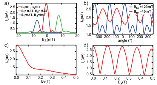
To obtain the CPR, we subtracted the average of over one period for every value of and , which corresponds to the switching current of the reference junction. This leaves us with the CPR.
Minima of as a function of
For a symmetric SQUID () with a sinusoidal CPR, one expects a like interference pattern of vs magnetic field. Therefore one would observe that fully vanishes at a magnetic flux equal to /2. If the SQUID is not symmetric, the supercurrent flowing in the two JJs will not fully compensate each other at /2, leaving us with a finite . But this observation is also possible if the CPR is not sinusoidal, even if the JJs are symmetric. To show that the non vanishing in the interference pattern in Fig.3 d of the article, is not only due to an asymmetry of the JJ, but rather given by a non sinusoidal CPR, we measured as a function of , while was fixed at 5 V and the in-plane magnetic field at -181.6 mT, which corresponds to a minimum of the interference pattern (see Fig.S5). When is tuned mainly the critical current carried by the top graphene layer changes. Like this it is possible to change between a symmetric and an asymmetric SQUID configuration. At the DP of the top layer ( V) the supercurrent is carried only by the bottom layer and the critical current is therefore only given by . When the gate voltage is increased, also increases. Since there is a phase difference of roughly /2 between the JJs due to the magnetic flux, the supercurrent flows in the opposite direction, which leads to a decrease of SQUID’s . This trend continues until , where will reach its minimum before it starts to increase again due to opposite asymmetry (). The non zero in the symmetric SQUID is attributed to the non sinusoidal CPR observed and discussed in the main text. This can be seen by taking a look how as a function of is calculated. First, the total supercurrent is given by , where () is the phase difference over the top (bottom) JJ and . For a given magnetic field is fixed but not the value of . To obtain now one has to maximize over . Therefore, to obtain a of zero, has to be zero for all . This is the case for the sum of two sinus curves shifted by /2 but is never the case if the CPRs are skewed sinusoidal functions. Therefore, the non vanishing supercurrent can be attributed to a non sinusoidal CPR.
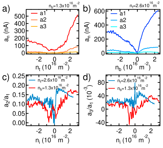
Gate dependence of
To fit the CPR we used Eq.3 in the article, which contains up to the fifth harmonic in frequency. If the CPR is sinusoidal to are all zero and only the first harmonic exists. The non-vanishing of the higher harmonic amplitudes indicates, that the CPR will be skewed and can be used as an alternative measurement quantity to the skewness (see main text) to define the deviation of the CPR from the sinusoidal behavior. For completion, we plot the to and the ratio between and , as well as the ratio between and in Fig.S7. The amplitudes and are much smaller then the the others and their contribution to skewness of the CPR can be neglected. For n (p) doped graphene a skewness of 0.25 (0.15) was extracted. This value corresponds to a ratio of / of around 0.15 (0.1).
Calculation of the interference pattern
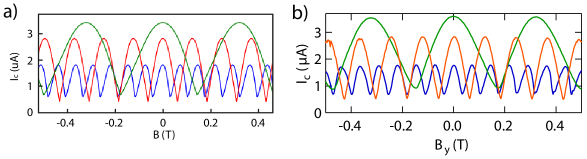
To get an idea of the asymmetry of the measurement shown in Fig.3 d of the main article, we calculated the in-plane magnetic field dependence of the . The CPRs were chosen to be equal and with skewness of =0.18, which is given by the choice of the prefactors , , and in Eq. 3 of the main text. The blue curve is the result of A and A, the red one for A and A and the green for A and A. For the blue result we took the dimension (junction length and middle hBN thickness) of J1, for the red the dimension of J2, and for the green curve the dimension of J3. The result reproduces qualitatively the measurements in Fig.S8 b. Therefore, we conclude that the in-plane magnetic field dependence of J2 was in a rather symmetric state of the SQUID, while for J1 and J3 the SQUID was slightly asymmetric. The calculations also reproduce the shape of the different curves.
Estimation of the loop inductance
The loop inductance () can lead to screening of the external magnetic field, which modifies the actual flux () inside the SQUID. Further it makes the relation between and the external flux () non linear. When the magnetic field axis is converted to a phase axis, this non linearity has to be taken into account, if or is large. In the case of a symmetric dc-SQUID, as a function of can be expressed by
| (15) |
Further, and defining the limit, at which the phase biasing by a magnetic field gets hysteretic. This limit is given by . To estimate the loop inductance, we calculated the kinetic inductance () of the MoRe leads and the geometric inductance () of the SQUID loop. The sum of these inductances results in .
was measured by the temperature dependence of the resonance frequency () of a /4-resonator.
| (16) |
where is the length of the resonator and is the kinetic inductance per unit length in the zero temperature limit. The geometric inductance of the resonator () as well as the geometric capacitance of the resonator () were calculated as described in Ref.12. We obtain a sheet inductance of =4.26 pH for a resonator thickness of 70 nm. is obtained by multiplying the sheet inductance with the interlayer distance, here =25 nm, and divide it by the the contacts width of 550 nm. By doing so =0.19 pH. Note, that this is an upper bound of the kinetic inductance, since the was determined using a 70 nm thick resonator. Here, due the supercurrent direction the thickness would correspond to the length of the contact region, which is about 850 nm. Therefore, we expect the kinetic inductance to be even smaller.
To estimate we calculate the inductance of a rectangular loop as derived in Ref.13. Here we take the following values: =, , =0.3 nm (thickness of graphene) and =1 nm the width of the of the loop. By taking equal to only 1 nm instead of the entire junction width, we get an upper limit of the geometrical inductance of =1.2 H. This has to be done since the used formula does not hold if is much larger then the product of and .
We calculate now the difference between and at , where the effect of the screening is the strongest. For a critical current of 3 A, the difference is not more then 0.3. Further, the maximal current, which can be passed through the SQUID before it starts to behave hysteretic is mA. For these reasons screening effects can be neglected in our measurements, since the measured critical currents are way smaller and the non linearity is not present.
References
- Ni et al. 2007 Ni, Z. H.; Wang, H. M.; Kasim, J.; Fan, H. M.; Yu, T.; Wu, Y. H.; Feng, Y. P.; Shen, Z. X. Graphene thickness determination using reflection and contrast spectroscopy. Nano Letters 2007, 7, 2758–2763
- Zomer et al. 2014 Zomer, P. J.; Guimaraes, M. H. D.; Brant, J. C.; Tombros, N.; Van Wees, B. J. Fast pick up technique for high quality heterostructures of bilayer graphene and hexagonal boron nitride. Applied Physics Letters 2014, 105, 1–4
- Indolese et al. 2018 Indolese, D. I.; Delagrange, R.; Makk, P.; Wallbank, J. R.; Watanabe, K.; Taniguchi, T.; Schönenberger, C. Signatures of van Hove Singularities Probed by the Supercurrent in a Graphene-hBN Superlattice. Physical Review Letters 2018, 121, 137701
- Handschin et al. 2017 Handschin, C.; Makk, P.; Rickhaus, P.; Liu, M. H.; Watanabe, K.; Taniguchi, T.; Richter, K.; Schönenberger, C. Fabry-Pérot resonances in a graphene/hBN Moiré superlattice. Nano Letters 2017, 17, 328–333
- Borzenets et al. 2016 Borzenets, I. V.; Amet, F.; Ke, C. T.; Draelos, A. W.; Wei, M. T.; Seredinski, A.; Watanabe, K.; Taniguchi, T.; Bomze, Y.; Yamamoto, M.; Tarucha, S.; Finkelstein, G. Ballistic Graphene Josephson Junctions from the Short to the Long Junction Regimes. Physical Review Letters 2016, 117, 1–5
- Dubos et al. 2001 Dubos, P.; Courtois, H.; Pannetier, B.; Wilhelm, F. K.; Zaikin, A. D.; Schön, G. Josephson critical current in a long mesoscopic S-N-S junction. Physical Review B 2001, 63, 1–5
- Ben Shalom et al. 2016 Ben Shalom, M.; Zhu, M. J.; Fal’ko, V. I.; Mishchenko, A.; Kretinin, A. V.; Novoselov, K. S.; Woods, C. R.; Watanabe, K.; Taniguchi, T.; Geim, A. K.; Prance, J. R. Quantum oscillations of the critical current and high-field superconducting proximity in ballistic graphene. Nature Physics 2016, 12, 318–322
- Amet et al. 2016 Amet, F.; Ke, C. T.; Borzenets, I. V.; Wang, Y.-M.; Watanabe, K.; Taniguchi, T.; Deacon, R. S.; Yamamoto, M.; Bomze, Y.; Tarucha, S.; Finkelstein, G. Supercurrent in the quantum Hall regime. Science 2016, 352, 966–969
- Steinigeweg et al. 2017 Steinigeweg, R.; Jin, F.; Schmidtke, D.; De Raedt, H.; Michielsen, K.; Gemmer, J. Real-time broadening of nonequilibrium density profiles and the role of the specific initial-state realization. Physical Review B 2017, 95, 1–6
- Couto et al. 2014 Couto, N. J.; Costanzo, D.; Engels, S.; Ki, D. K.; Watanabe, K.; Taniguchi, T.; Stampfer, C.; Guinea, F.; Morpurgo, A. F. Random strain fluctuations as dominant disorder source for high-quality on-substrate graphene devices. Physical Review X 2014, 4, 1–13
- Kim et al. 2019 Kim, Y.; Herlinger, P.; Taniguchi, T.; Watanabe, K.; Smet, J. H. Reliable Postprocessing Improvement of van der Waals Heterostructures. ACS Nano 2019, 13, 14182–14190
- Gevorgian 1994 Gevorgian, S. Basic characteristics of two layered substrate coplanar waveguides. Electronics Letters 1994, 30, 1236–1237
- Shatz and Christensen 2014 Shatz, L. F.; Christensen, C. W. Numerical Inductance Calculations Based on First Principles. PLoS ONE 2014, 9