A Direct Mapped Method for Accurate Modeling and Real-Time Simulation of High Switching Frequency Resonant Converters
Abstract
This paper presents a Direct Mapped Method (DMM) for real-time simulation of high switching frequency resonant converters. The DMM links state variables to diode statuses and provides an exact and noniterative solution to network equations. The proposed method is implemented on FPGA to simulate an LLC converter with switching frequencies ranging up to 500 kHz. The best reported implementations of DMM achieve a 25 ns simulation time-step for a wide range of clock frequencies, ranging from 40 MHz to 320 MHz.
Index Terms:
Real-time simulation, FPGA, high switching frequency converters, resonant converters, power electronic converter modeling.I Introduction
AAdvances in semiconductor technology allow the increase of the efficiency and power density of modern power electronic converters (PECs) by operating them at higher switching frequencies (50 kHz). Resonant converters are particularly of interest and renowned for their higher power density with typically small L/C components [1, 2]. These converters are typically operated using soft switching techniques to preclude switching losses, reduce filtering requirements, and to mitigate electromagnetic interference (EMI) [3, 4]. Among various resonant topologies [5], the LLC converter has drawn attention for its unique characteristics such as low voltage stress on the secondary rectifier and high efficiency at high input voltages [6, 7].
These technology advancements are however very challenging for the realm of FPGA-based Hardware-In-the-Loop (HIL) real-time simulation (RTS). HIL simulation is a prototyping technique used to assess the performance of control/protection systems in the design or installation stages. FPGAs are programmable devices that have played a pivotal role during the last decade in the RTS of PECs for HIL applications [8, 9, 10]. The main challenges faced by the FPGA-based HIL of high switching frequency (HSF) converters come from the limited memory resources and the heavy processing requirements given the small calculation time-step.
Two main modeling approaches are typically employed in FPGA-based RTS to model switching devices: i) The Associate Discrete Circuit (ADC); and ii) The Resistive Switch Model (RSM). The ADC switch model was introduced in the 90s [11] and has been since extensively utilized for RTS applications, provided that the simulation time-step () is sufficiently small[8, 9, 10]. However, ADC is prone to fictitious oscillations that can alter the behavior of a PEC model in particular when dealing with HSF. Various techniques exist to alleviate these drawbacks [12, 13, 14, 15], but are unpractical for resonant converters because the adopted switch model affects the resonant tank behaviour. The RSM on the other hand uses a two-valued resistance for the switch ( and ) [16, 17, 18, 19, 20]. RSM produces more accurate results compared to ADC when modeling PECs, but has the drawbacks of a variable admittance matrix and heavier computations in real-time.
To circumvent the heavy computational burden of RSM, the inverse of the nodal matrix for all possible switch combinations can be precomputed. This approach, however, considerably limits the number of switches due to FPGA memory requirement limitations. The Sherman-Morrison-Woodbury formula has been utilized to compute the updated inverse matrix on the fly [18], but the method is unpractical for HSF PECs, and neglects the iterations needed to determine the state of natural commutation devices such as diodes. Methods for handling the RTS of diodes can be found in [16, 17, 20, 19]. In [16], unrealistic parasitic elements are augmented in parallel with switches that may alter the behavior of the converter, more so when resonant converters are considered. The method proposed in [17] results in large time-steps and as such is inadequate for the simulation of HSF PECs. A predictor-corrector algorithm has been used in [19] to decouple the switches from the circuit elements and to simulate them simultaneously. However, due to the stability concerns, very short time-steps should be selected which results in increased hardware resources when dealing with large circuits. More recently, the RSM has been used to simulate low-frequency PECs [20]. This method, however, uses an iterative solver to deal with switches, which makes it unpractical for the simulation of HSF PECs.
The RTS of HSF converters is more challenging since it requires very small time-steps which can be restrictive for the iterative solver. To obviate the iterative procedure while adopting the RSM, some specific simplifications are often made for the determination of switch states. In [21], a commercial RTS method has been used to simulate an LLC, with the switching frequency of 20 kHz which is relatively low. The simulation of an LLC converter with a switching frequency of 60 kHz has been presented in [22], where the LLC model is built by breaking down the converter into interconnected modules. This approach relies on intra-module delays which can cause erroneous results. In [23], an LLC converter with a resonance frequency of 160 kHz has been simulated using FPGA. The simulations have been done by making use of Forward Euler (FE) method where a time-step of 15 ns has been achieved. The FE is not however a generic approach and might not work for certain LLC parameters. This will be discussed for the first time in this paper.
This paper proposes a Direct Mapped Method (DMM) for accurate RSM-based simulation of HSF resonant converters. The method offers higher computational performance while providing the same level of accuracy compared to iterative solutions. The DMM proceeds by constructing a mapping function that relates the state variables of the circuit to switch states. The mapping function is then used to directly determine switch states during the simulation. In this paper, the DMM is used to implement an FPGA-based LLC simulator with parameters taken from the literature. It is demonstrated that the method is successful in the accurate simulation of LLC converters with switching frequencies ranging up to 500 kHz.
The remainder of this paper is organized as follows. The theoretical background of resonant and LLC converters are briefly presented in Section II. In Section III, the DMM is elaborately presented while its application for an LLC converter is discussed. Section IV presents the FPGA implementation of the DMM and discusses experimental results.
II DC-DC Resonant Converter
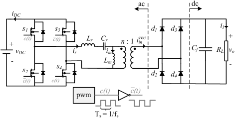
A typical DC-DC resonant converter is comprised of three stages: an inverter, a 2- or 3-element resonant tank, and a rectifier. The inverter consists of a MOSFET half-bridge or full-bridge, operated with a fixed 50% duty cycle. The power flow of the converter is controlled by modulating the frequency of the square wave with respect to the tank’s resonant frequency. The rectifier stage converts its AC input to a DC output voltage which is filtered by a capacitor. A transformer is often used in the rectification stage for scaling and isolation purposes.
The resonant tank modulates the voltage using L-C elements such as series LC, parallel LC, LLC, etc. These resonant tanks are selected depending on the converter application [24]. In this work, we will focus on the LLC converter topology which is comprised of a full-bridge inverter and a full-bridge rectifier, see Fig. 1. The LLC converter is used in many applications such as power electronic-based distributed generation, electric vehicles, computer and communication systems [25, 26, 27, 28]. The proposed DMM is, however, applicable to other resonant topologies as well.
II-A Overview of the LLC Resonant Converter
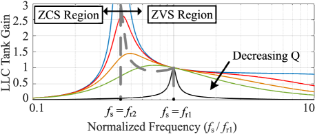
The LLC converter is a multi-resonant converter with resonant frequencies and . With reference to Fig. 1, is embodied in the magnetizing inductance of the transformer which helps to reduce the size and the cost of the the converter[26]. LLC resonant tank gain, , is defined as the magnitude of its input–output voltage transfer function. Typical voltage gains of the LLC tank for different normalized switching frequencies , ( being the switching frequency) are obtained from [29]:
| (1) |
where is the quality factor, and is the inductance ratio:
| (2) |
denotes the reflected load resistance , seen from the resonant tank side, and is the turn ratio of the isolation transformer.
II-B LLC Operation
Fig. 2 depicts the LLC voltage gain for different values of quality factor , which are used for the analysis and design of the resonant converter. delimits the capacitive and the inductive regions of the resonant tank, which are associated with the Zero Current Switching (ZCS) and Zero Voltage Switching (ZVS) regions, respectively. The MOSFET-based LLC converters are preferably operated in the ZVS region, i.e. , since it significantly mitigates the switching losses[5]. When LLC is working with , at the end of one half resonant cycle, during a certain time interval no power is delivered to the load and the whole resonant current passes through the magnetizing inductance. During this time interval, the rectifier is said to be in blocking mode (). The region where refers to an operational mode of the LLC where a resonant half cycle is not completed and interrupted by the switching of other MOSFET.
II-C LLC Simulation
In this paper, the LLC converter of Fig. 1 is considered for which two sets of parameters are chosen from the literature as listed in Table I. In this table, LLC with Parameter Set #1 [23] and Parameter Set #2 [30] has the resonant frequency of 160 kHz, 500 kHz, respectively. We will show in this section why an iterative solution is needed to accurately simulate the LLC converter.
As proposed in [19] and [23], an explicit integration method such as FE can be used to avoid the iterative process. This however necessitates adopting a sufficiently small simulation time-step. For the sake of clarity, let us recall that FE offers a recursive solution to in the following form:
| (3) |
By applying Eq. (3) to the resonant inductors of the resonant tank of the LLC, an explicit expression for the rectifier’s input current is obtained (see Fig. 1):
| (4) |
It is proposed in [23] to use Eq. (4) to determine the mode of the full-bridge rectifier; positive mode when , , and negative mode otherwise — . However, such an approach may lead to either inaccurate results or instability, even for very small time-steps. This behavior is partly due to the fact that this method completely ignores the blocking mode of the converter.

| Parameter | Parameter Set #1[23] | Parameter Set #2 [30] |
| (kHz) | 160 | 500 |
| (kHz) | 60 | 210 |
| :1 | 1.5:1 | 33:1 |
| (V) | 600 | 400 |
| (V) | 400 | 12 |
| (H) | 25 | 4.5 |
| (H) | 150 | 21.6 |
| (nF) | 40 | 22 |
| (F) | 1000 | 3000 |
| P(kW) | 5.3 | 1 |
| () | 30 | 0.144 |
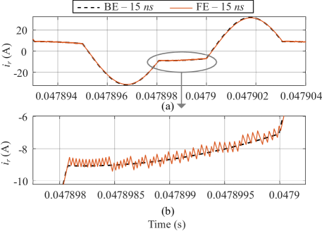
Fig. 3.a gives the resonant current, , for LLC with Parameter Set #1 (see Table I), calculated by either making use of FE or backward Euler (BE) methods, and assuming a time-step of 15 ns. It is noted that BE method is applied through an iterative solution. The zoomed view of resonant current during the blocking mode is shown in Fig. 3.b. It is seen from this figure that in contrast with BE method, the current calculated by the method proposed in [23] is oscillatory during the blocking mode period. The blocking mode is in fact disregarded during the simulation i.e., only positive and negative modes are considered, and the model alternates between the two modes during the blocking period.
The effects of ignoring the blocking mode for LLC with Parameter Set #2 (see Table I) are observed in Fig. 4. Similar to the previous case, is calculated by either BE or FE with the same 15 ns time-step. It is seen from Fig. 4 that calculated by FE is oscillatory during the blocking mode. It is also seen from Fig. 4 that, as opposed to LLC with Parameter Set #1, the results of FE and BE are quite different for LLC with Parameter Set #2. This indicates that the accuracy of the method proposed in [23] can be affected by circuit parameters.
During our simulations, it was also observed that the resonant current calculated by FE method becomes unstable for ns. It is also worth noting that another possible mode of the rectifier stage of the LLC circuit of Fig. 1 is the short circuit mode, i.e. which is also disregarded by explicit methods such as[23, 19].
III Direct Mapped Method
III-A DMM Analysis of the LLC
Without losing any generality, we consider the circuit of Fig. 5, which represents the rectifying stage of the LLC. Both AC and DC side circuits are replaced by a Norton equivalent circuit comprised of a conductance in parallel with a time-dependent current source. The Norton equivalents result from the BE discretizition.
The following systems of equations associate network equations of the circuit of Fig. 5 using a classical nodal analysis:
| (5) |
|
, |
(6) |
| (7) |

where is the admittance matrix, refers to the 16 diodes status combinations, is the unknown nodes voltages and is the current injection vector. , are the conductances associated with the diodes ( or , with respect to the diode status combination ).
Eq. (5) can be rewritten as:
| (8) |
| (9) |
| (10) |
In addition, diodes voltages can be defined using a connectivity matrix, , as:
| (11) |
| (12) |
| (13) |
The RSM requires the correct state of each diode (ON/OFF) at each time-point. This is done by checking whether the sign of the diode’s voltage or its current () is positive or negative. However, from (13), one can find that diode conducts whenever , :
| (14) |
| (15) |
| (16) |
| (17) |
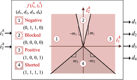
Hence, for each combination , a system of inequalities combining (14)-(17) is obtained, and the Fourier-Motzkin elimination [31] is used to evaluate its feasibility.
The feasibility check reveals that only 4 feasible diode combinations exist, those for which and . A mapping function linking the state variables to diode states, , can be obtained. Fig. 6 demonstrates this mapping function in the -plane with four half lines dividing the plane into four feasible regions: (0, 0, 0, 0) = Blocked, (1, 0, 0, 1) = Positive, (0, 1, 1, 0) = Negative and (1, 1, 1, 1) = Shorted. The half lines start at the origin and have slopes of and , as illustrated in Fig. 6. The slopes and are given by:
| (18) |
| (19) |
| (20) |
| (21) |
Assuming , slope is approximated by:
| (22) |
From (22), one can observe that the slope (which delimits the Blocked from the Positive and Negative states) is approximately independent of diode conductances and is a function of both AC and DC side parameters. It also appears from Eq. (22) that explicit solvers such as those used in [19, 23] — which substitute the Norton equivalent of the AC side by a pure current source () — discard the Blocked mode of the rectifier because they force to infinity. Such an approximation is not problematic if the slope is very large such as for Parameter Set #1, but can considerably degrade the simulation results for other parameters, such as those of Parameter Set #2.
III-B Simulation Algorithm
The aim of this section is to develop a simulation algorithm for the LLC converter of Fig. 1. The inverter is operated in controlled mode, and DMM is used to determine the diode states. Network equations for the LLC converter of Fig. 1 are formulated using the Modified Augmented Nodal Analysis (MANA) [32] after discretizing all elements using BE rule:
| (23) |
where is the MANA matrix for switch combination , is the incidence matrix, is the vector of unknown variables. is the input DC voltage, , and are ac and dc side history vectors, respectively. is comprised of node voltages (), the current entering the DC voltage source () and the current entering the secondary port of the transformer (): . The history vectors are comprised of the history currents that result from the backward discretization of the L/C components in the circuits: , and . More on the use of MANA for the simulation of power electronic circuits can be found in [17, 33].
To reduce the computational burden of solving Eq. (23) at each time-point of the simulation, the following formulation is used:
| (24) |
where are precomputed matrices obtained from simple algebraic manipulations of and inverse of . is a vector comprised of desired output variables, . Similar rewritings are used to determine the history currents associated with the Norton equivalents of the ac and dc sides:
| (25) |
where is the switch combination associated with the inverter’s state, which is defined as a function of the gating signal driving and (see Fig. 1), given the controlled operation of the inverter:
| (26) |
The DMM function is used to determine and :
| (27) |
| (28) |
DMM consists mainly in solving the following (see Fig. 6):
| (29) |
where is the sign function. The DMM function reads henceforth as follows:
| (30) |
From the mathematical formulation given above, the following algorithm is used at each time-point to simulate the LLC:
- 1.
- 2.
-
3.
Compute the output vector as well as the history vectors and for the next time-point using Eq. (24).
This algorithm is referred to as the Two-Stage Algorithm because it involves two Matrix-Vector Multiplications (MVMs): Step 1) is performed by combining Eqs. (25), (29) into a single MVM following which Eq. (30) is used to determine . Step 2) is a simple binary word concatenation and is therefore instantaneous. Step 3) constitutes the second stage MVM of the algorithm.
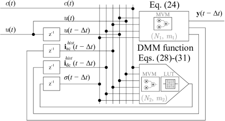
III-C Low-latency Implementation of the DMM

Fig. 7.a illustrates a dataflow diagram for the Two-Stage Algorithm, and shows the data dependency of the two stages (through ) that forces their serial execution. Moreover, each stage involves matrix vector multiplications (MVMs) that hinders reaching to a small time-step.
It is possible to reduce the time-step if one rewrites Eqs. (25) in the following form:
| (31) |
Hence, knowing , , , , , and would suffice to determine . Fig. 7.b illustrates how this rewriting yields a Single-Stage Algorithm version of the DMM by breaking the data dependency. The only limitation of this approach is that two consecutive simulation steps are needed to produce the output vector . Section IV will demonstrate that the hardware implementation of the Single-Stage results in an input-output latency of two time-steps, but that it is legitimate since the simulation time-step is halved compared to the Two-Stage version of the algorithm.
IV FPGA Implementation

IV-A Hardware Implementation
A hardware implementation of the Single-Stage DMM algorithm datapath is shown in Fig. 8. The architecture is almost a one to one map of the dataflow diagram of Fig. 7.b, and consists of two main computing units: a) The first unit is devoted to updating history terms and computing outputs of interest, i.e. Eq. (24); b) The second unit evaluates the DMM function, i.e. Eqs. (28)-(31). Eq. (24) is implemented by a dedicated MVM module; Eqs. (29) and (31) are combined and implemented by a dedicated MVM module as well. Eqs. (30) is a simple lookup table. Eq. (28) consists of a bit string concatenation and comes at no hardware cost.
IV-B Number Format
An FPGA can handle real arithmetic using either fixed-point (FXP) or floating-point (FP) format. The FXP format uses less hardware and yields a datapath of lower latency, but has a limited dynamic range. The FP number format allows for a larger dynamic range, but its hardware arithmetic operators are costly in terms of FPGA resource consumption, and require deeper pipelines than their FXP counterparts. Due to latency considerations, this paper considers solely the FXP number format. The limited dynamic range issue of the FXP format is addressed by normalizing matrix entries using a per-unit scale.
The targeted FPGA, a Kintex K325T from Xilinx, uses an asymmetric multiplication block ( signed). Hence, the selected number format used by the LLC simulator will be different whether we are dealing with a vector (FXP 25.23) or a matrix (FXP 35.29) in order to offer a good precision to the precomputed matrices and good computation accuracy, while reducing the area footprint of the simulator. A similar idea was presented in [16] and is adopted here.
| Item | 40 MHz | 200 MHz | 320 MHz | |
|---|---|---|---|---|
| FPI | Min. Time-Step | 25 ns | 25 ns | 25 ns |
| In-Out Latency | 50 ns | 50 ns | 50 ns | |
| Registers | 1,224 (0.3%) | 1,697 (0.4%) | 2,373 (0.6%) | |
| LUTs | 1,090 (0.5%) | 1,095 (0.5%) | 1,223 (0.6%) | |
| DSP Blocks | 88 (10.5%) | 88 (10.5%) | 88 (10.5%) | |
| BRAM | 22 (4.9%) | 22 (4.9%) | 22 (4.9%) | |
| HRT | Min. Time-Step | 100 ns | 40 ns | 34.375 ns |
| In-Out Latency | 200 ns | 80 ns | 68.750 ns | |
| Registers | 211 (0.1%) | 350 (0.1%) | 498 (0.1%) | |
| LUTs | 277 (0.1%) | 329 (0.2%) | 311 (0.2%) | |
| DSP Blocks | 22 (2.6%) | 22 (2.6%) | 22 (2.6%) | |
| BRAM | 5.5 (1.2%) | 5.5 (1.2%) | 5.5 (1.2%) |
IV-C Design Space Exploration
This section presents a design space exploration whose purpose is to evaluate the impact of parameters and on area occupation, and simulation time-step. Two implementations are considered in this design exploration, the first approach consists in a Fully Parallel Implementation (FPI) that sets , and ; whereas the second approach will resort to a Hardware Reuse Technique (HRT) that consists in setting and , thus time-multiplexing the computations. In this paper, the adopter HRT approach sets and .
Also considered is the effect of the FPGA clock frequency on the timing performance and simulation time-step. Various clock frequencies are investigated, namely 40 MHz, 200 MHz and 320 MHz. The timing closure is met by varying the pipelining depth of the DP Unit accordingly. When the 40 MHz clock frequency is targeted, the DP Unit is purely combinational.
Table II presents the design exploration results for the Kintex K325T for each design approach and each target frequency. It shows that the smallest simulation time-steps (25 ns) are obtained when a FPI approach is adopted. FPI is however the most expensive approach in terms of hardware consumption. The HRT trades simulation time-step for area footprint. Hence, this approach allows considerable saving in hardware utilization (up to 4 folds), with a very acceptable impact on the simulation time-steps, which are less or equal to 100 ns. For HRT, smaller time-steps are achieved by increasing the clock frequency, with the smallest time-step (34.375 ns) obtained for the highest clock frequency (320 MHz). The 200 MHz implementations are the most balanced options for both FPI and HRT approaches.
That being said, all reported implementations are characterized by a very low hardware utilization, a small simulation time-step ( 100 ns), and an input-output (In-Out) latency of two time-steps. These notable results are more obvious from Table III, which lists from the literature works dealing with the real-time simulation of high-frequency converters, i.e. 50 kHz. As one can see from Table III, where the 200 MHz FPI and HRT results have been reproduced, the proposed implementations have indeed a very small footprint and offer one of the smallest time-steps ever reported in the literature. It is noteworthy that, thanks to the proposed DMM, these outcomes are obtained using an implicit solver, without decoupling any part of the circuit, and while using a simultaneous and exact switch state solution.
Power Electronic Circuit FPGA Resource Consumption (ns) Solver Application Sw. Frq. (kHz) FPGA Clk (MHz) Number Format LUTs Registers BRAM DSP48 FPI 25 BE LLC 500 K7-3251 320 FXP 32.29/25.22 1,095 (0.5%) 1,697 (0.4%) 22 (4.9%) 88 (1.05%) HRT 40 BE LLC 500 K7-3251 320 FXP 32.29/25.22 329 (0.2%) 350 (0.1%) 5.5 (1.2%) 22 (2.6%) [23] 15 FE Batt. Charger 160 K7-4102 66.67 FXP 25.23 45,560 (17.9%) 44,277 (8.7%) 106 (13.3%) 43 (2.8%) [18] 36 BE AC-DC-AC 50 V7-4853 200 SFP4 116,670 (38%) 68,920 (11%) 1,202 kb (3%) 762 (27%) [22] 100 FE LLC 60 NR6 NR NR NR NR NR NR [34] 40 PC5: FE-BE NPC NR K7-4102 25 32 47,028 (25.8%) 42,642 (11.2%) 91 (11.6%) 120 (17.7%) [35] 40 Sw. fct + FE Batt. charger 100 ZYNQ 200 FXP 32.20 NR NR NR NR [16] 80 BE 3- inverter 200 V5-507 200 FXP 35.30/25.16 229 (7%) 3,531 (10.8%) 44 (33.3%) 176 (61.1%) [36] 50 Sw. fct + FE 3- inverter 100 V7-4853 200 FXP 72.43 3,943 (1.3%) 893 (0.1%) NR 170 (6.1%) 1K7-325: Kintex XC7K325T. 2K7-410: Kintex XC7K410T. 3V7-485: Virtex XC7VX485T 4SFP: Single precision FP. 5PC: Predictor-Corrector. 6NR: Not Reported. . 7V5-50: Virtex VC5VSX50T.
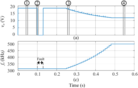
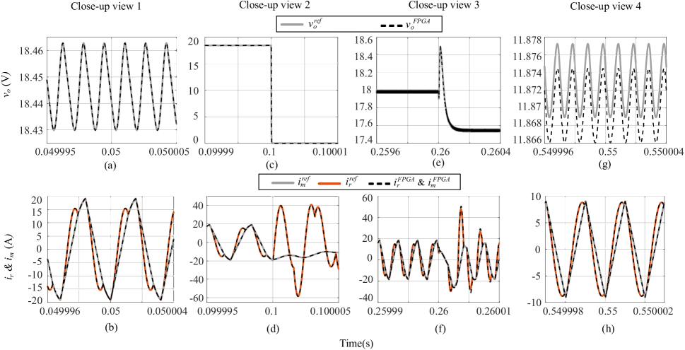
IV-D Computational Accuracy
The computational accuracy of the hardware LLC simulator (200 MHz FPI) is assessed through a test sequence lasting 0.6s. Parameter Set #2 in Table I is considered. During the test sequence, the input voltage is kept constant at 400 V. The FPGA simulation results are validated against an offline iterative solution, as shown in Fig. 10, where the output voltage () and the switching frequency are shown. The test sequence comprises the following steps:
-
1.
s-s: Operation of the inverter at kHz.
-
2.
s-s: Load is shorted (fault); kHz.
-
3.
s-s: Fault cleared; kHz.
-
4.
s-s: The switching frequency is increased from kHz to kHz.
-
5.
s-s: Operation at kHz.
From Fig. 10, one can see that the gradually decreases and finally settles at 12 V as is increased from kHz to kHz. Fig. 11 offers close-up views of four instants, as identified in Fig. 10. The FPGA results are overlapped in the same figure and show very good agreements with the reference. At 500 kHz, the output voltage shows a slight dc offset (Fig. 11.g) that is not larger that 0.2%.
| Sequence | |||
|---|---|---|---|
| 0.00s-0.10s | 0.024% | 0.383% | 0.120% |
| 0.10s-0.13s | 0.001% | 0.001% | 0.016% |
| 0.13s-0.25s | 0.021% | 0.338% | 0.131% |
| 0.25s-0.48s | 0.006% | 0.391% | 0.131% |
| 0.48s-0.60s | 0.023% | 0.499% | 0.048% |
| 0.00s-0.60s | 0.018% | 0.336% | 0.124% |
To further assess the accuracy of the FPGA result, each signal is compared to its offline reference. The 2-norm relative error is used as a measure of accuracy [37]:
| (32) |
where and are FPGA results and offline reference, respectively. Table IV reports the 2-norm errors for the FPGA results for each sub-sequence as well as for the entire test sequence. All the reported errors are below 0.5% and show the very good performance of the FPGA implementation in different operating mode and condition of the LLC.
V Conclusion
This paper presented a direct mapped method for the accurate real-time simulation of high switching frequency resonant converters. The method obviates the need for iterations while providing accurate simulation results. The benefits of the proposed method was demonstrated through the implementation of an FPGA-based LLC real-time simulator capable of achieving a time-step of 25 ns while offering a very small hardware footprint. A design space exploration was proposed to discuss the opportunity of further reducing the area occupation by reusing parts of the computational datapath. It was shown that such an approach can result in considerable savings for higher clock frequencies. The LLC simulator performance has been evaluated for the case of a 500 kHz LLC converter. It has been shown that the DMM real-time results are in excellent agreement with those obtained by offline iterative solution. A 2-norm relative error of less than 0.5% for various operating modes has been reported, which was also shown to hold true in the presence of a fault.
References
- [1] R. C. N. Pilawa-Podgurski, A. D. Sagneri, J. M. Rivas, D. I. Anderson, and D. J. Perreault, “Very-high-frequency resonant boost converters,” IEEE Trans. Power Electron., vol. 24, no. 6, pp. 1654–1665, 2009.
- [2] N. C. D. Pont, D. G. Bandeira, T. B. Lazzarin, and I. Barbi, “A ZVS APWM half-bridge parallel resonant DC–DC converter with capacitive output,” IEEE Trans. Ind. Electron., vol. 66, no. 7, pp. 5231–5241, Jul. 2019.
- [3] M. D. Bellar, T. S. Wu, A. Tchamdjou, J. Mahdavi, and M. Ehsani, “A review of soft-switched DC-AC converters,” IEEE Trans. Ind. Appl., vol. 34, no. 4, pp. 847–860, 1998.
- [4] X. Fang, H. B. Hu, F. Chen, U. Somani, E. Auadisian, J. Shen, and I. Batarseh, “Efficiency-oriented optimal design of the LLC resonant converter based on peak gain placement,” IEEE Trans. Power Electron., vol. 28, no. 5, pp. 2285–2296, 2013.
- [5] R. W. Erickson and D. Maksimovic, Fundamentals of Power Electronics, 2nd ed. Springer US, 2001.
- [6] Bo Yang, F. C. Lee, A. J. Zhang, and Guisong Huang, “LLC resonant converter for front end DC/DC conversion,” in Appl. Power Electron. Conf. Expo. (APEC), pp. 1108–1112, Mar. 2002.
- [7] X. Xie, J. Zhang, C. Zhao, Z. Zhao, and Z. Qian, “Analysis and optimization of LLC resonant converter with a novel over-current protection circuit,” IEEE Trans. Power Electron., vol. 22, no. 2, pp. 435–443, 2007.
- [8] M. Matar and R. Iravani, “FPGA implementation of the power electronic converter model for real-time simulation of electromagnetic transients,” IEEE Trans. Power Del., vol. 25, no. 2, pp. 852–860, 2010.
- [9] T. Ould-Bachir, C. Dufour, J. Bélanger, J. Mahseredjian, and J. David, “A fully automated reconfigurable calculation engine dedicated to the real-time simulation of high switching frequency power electronic circuits,” Mathematics and Computers in Simulation, vol. 91, pp. 167–177, 2013.
- [10] M. Dagbagi, A. Hemdani, L. Idkhajine, M. W. Naouar, E. Monmasson, and I. Slama-Belkhodja, “ADC-based embedded real-time simulator of a power converter implemented in a low-cost FPGA: Application to a fault-tolerant control of a grid-connected voltage-source rectifier,” IEEE Trans. Ind. Electron., vol. 63, no. 2, pp. 1179–1190, Feb. 2016.
- [11] P. Pejovic and D. Maksimovic, “A method for fast time-domain simulation of networks with switches,” IEEE Trans. Power Electron., vol. 9, no. 4, pp. 449–456, 1994.
- [12] R. Razzaghi, C. Foti, M. Paolone, and F. Rachidi, “A method for the assessment of the optimal parameter of discrete-time switch model,” Electric Power Systems Research, vol. 115, pp. 80–86, 2014.
- [13] K. Wang, J. Xu, G. Li, N. Tai, A. Tong, and J. Hou, “A generalized associated discrete circuit model of power converters in real-time simulation,” IEEE Trans. Power Electron., vol. 34, no. 3, pp. 2220–2233, Mar. 2019.
- [14] Q. Mu, J. Liang, X. Zhou, Y. Li, and X. Zhang, “Improved ADC model of voltage-source converters in dc grids,” IEEE Trans. Power Electron., vol. 29, no. 11, pp. 5738–5748, Nov. 2014.
- [15] C. Dufour, “Method and system for reducing power losses and state-overshoots in simulators for switched power electronic circuit,” U.S. Patent 9,665,672, May 30, 2017.
- [16] H. F..-Blanchette, T. Ould-Bachir, and J. P. David, “A state-space modeling approach for the FPGA-based real-time simulation of high switching frequency power converters,” IEEE Trans. Ind. Electron., vol. 59, no. 12, pp. 4555–4567, 2012.
- [17] T. Ould-Bachir, H. F.-Blanchette, and K. Al-Haddad, “A network tearing technique for FPGA-based real-time simulation of power converters,” IEEE Trans. Ind. Electron., vol. 62, no. 6, pp. 3409–3418, 2015.
- [18] A. Hadizadeh, M. Hashemi, M. Labbaf, and M. Parniani, “A matrix-inversion technique for FPGA-based real-time emt simulation of power converters,” IEEE Trans. Ind. Electron., vol. 66, no. 2, pp. 1224–1234, Feb. 2019.
- [19] C. Liu, H. Bai, S. Zhuo, X. Zhang, R. Ma, and F. Gao, “Real-time simulation of power electronic systems based on predictive behavior,” IEEE Trans. Ind. Electron., pp. 1–1, 2019.
- [20] R. Mirzahosseini and R. Iravani, “Small time-step FPGA-based real-time simulation of power systems including multiple converters,” IEEE Trans. Power Del., vol. 34, no. 6, pp. 2089–2099, Dec. 2019.
- [21] D. Siemaszko, L. de Mallac, S. Pittet, and D. Aguglia, “Modular resonant converter for 25kV-8A power supply: Design, implementation and real time simulation,” in European Conference on Power Electronics and Applications (EPE), pp. 1–10, Aug. 2014.
- [22] Fan Ji, Hongtao Fan, and Yaojie Sun, “Modelling a FPGA-based LLC converter for real-time hardware-in-the-loop (HIL) simulation,” in International Power Electronics and Motion Control Conference (IPEMC), pp. 1016–1019, May. 2016.
- [23] H. Bai, H. Luo, C. Liu, D. Paire, and F. Gao, “Real-time modeling and simulation of electric vehicle battery charger on FPGA,” in International Symposium on Industrial Electronics (ISIE), pp. 1536–1541, Jun. 2019.
- [24] D. Huang, F. C. Lee, and D. Fu, “Classification and selection methodology for multi-element resonant converters,” in Appl. Power Electron. Conf. Expo. (APEC), pp. 558–565, Mar. 2011.
- [25] X. Sun, Y. Shen, Y. Zhu, and X. Guo, “Interleaved boost-integrated LLC resonant converter with fixed-frequency PWM control for renewable energy generation applications,” IEEE Trans. Power Electron., vol. 30, no. 8, pp. 4312–4326, 2015.
- [26] L. E. Zubieta and P. W. Lehn, “A high efficiency unidirectional dc/dc converter for integrating distributed resources into DC microgrids,” pp. 280–284, 2015.
- [27] W. Haoyu, S. Dusmez, and A. Khaligh, “Design and analysis of a full-bridge LLC-based PEV charger optimized for wide battery voltage range,” IEEE Trans. Veh. Technol., vol. 63, no. 4, pp. 1603–1613, 2014.
- [28] H. Li, Z. Zhang, S. Wang, J. Tang, X. Ren, and Q. Chen, “A 300-khz 6.6-kw SiC bidirectional LLC on-board charger,” IEEE Trans. Ind. Electron., vol. 67, no. 2, pp. 1435–1445, Feb. 2020.
- [29] S. Abdel-Rahman, “Resonant LLC converter: Operation and design,” Infineon Technologies North America (IFNA), Tech. Rep. AN 2012-09, September 2012.
- [30] C. Fei, Q. Li, and F. C. Lee, “Digital implementation of light-load efficiency improvement for high-frequency LLC converters with simplified optimal trajectory control,” IEEE Trans. Emerg. Sel. Topics Power Electron., vol. 6, no. 4, pp. 1850–1859, Dec. 2018.
- [31] J. Matouek and B. Gärtner, Understanding and Using Linear Programming. Berlin, Heidelberg: Springer-Verlag, 2006.
- [32] J. Mahseredjian, S. Dennetière, L. Dubé, B. Khodabakhchian, and L. Gérin-Lajoie, “On a new approach for the simulation of transients in power systems,” Electric Power Systems Research, vol. 77, no. 11, pp. 1514–1520, 2007, selected Topics in Power System Transients - Part II.
- [33] F. Montano, T. Ould-Bachir, and J. P. David, “An evaluation of a high-level synthesis approach to the FPGA-based submicrosecond real-time simulation of power converters,” IEEE Transactions on Industrial Electronics, vol. 65, DOI 10.1109/TIE.2017.2716880, no. 1, pp. 636–644, Jan. 2018.
- [34] C. Liu, H. Bai, R. Ma, X. Zhang, F. Gechter, and F. Gao, “A network analysis modeling method of the power electronic converter for hardware-in-the-loop application,” IEEE Transactions on Transportation Electrification, vol. 5, no. 3, pp. 650–658, Sep. 2019.
- [35] T. Gherman, D. Petreus, and R. Teodorescu, “A real time simulator of a pev’s on board battery charger,” in 2019 International Aegean Conference on Electrical Machines and Power Electronics (ACEMP) 2019 International Conference on Optimization of Electrical and Electronic Equipment (OPTIM), pp. 329–335, Aug. 2019.
- [36] M. Milton, A. Benigni, and J. Bakos, “System-level, FPGA-based, real-time simulation of ship power systems,” IEEE Trans. Energy Convers., vol. 32, no. 2, pp. 737–747, Jun. 2017.
- [37] W. Gautschi, Numerical analysis : an introduction. MA, Boston: Birkhauser, 1997.
| Hossein Chalangar received the B.Sc. and M.Sc degrees in electrical engineering from K. N. Toosi University of Technology (KNTU), Tehran, Iran, in 2011 and 2013, respectively. He is currently working toward the Ph.D. degree at Polytechnique Montréal, Canada. His research interests include real-time simulation of power systems and power electronics. |
| Tarek Ould-Bachir (M’08) received the M.A.Sc. and Ph.D. degrees in electrical engineering from the Polytechnique Montréal, Montreal, QC, Canada, in 2008 and 2013, respectively. From 2007 to 2018, he was with OPAL-RT Technologies, holding various positions in the R&D department. From 2018 to 2020, he was a Research Associate with Polytechnique Montréal. He is currently an Assistant Professor with Polytechnique Montréal. |
| Keyhan Shesheykani (M’10-SM’13) received the B.S. degree in electrical engineering from Tehran University, Tehran, Iran, in 2001, and the M.S. and Ph.D. degrees in electrical engineering from Amirkabir University of Technology (Tehran Polytechnique), Tehran, Iran in 2003 and 2008, respectively. He was with Ecole Polytechnique Fédérale de Lausanne, Lausanne, Switzerland, in September 2007 as a Visiting Scientist and later as a Research Assistant. From 2010 to 2016, he was with Shahid Beheshti University, Tehran. He was an Invited Professor at the EPFL from June to September 2014. He joined the Department of Electrical Engineering, Polytechnique Montréal, Montreal, QC, Canada, in 2016, where he is currently an Associate Professor. Dr. Sheshyekani currently serves as the Associate Editor of IEEE Transactions on Electromagnetic Compatibility. His research interests include power system modeling and simulation, smart grids and electromagnetic compatibility. |
| Jean Mahseredjian (F’13) received the M.A.Sc. and Ph.D. degrees in electrical engineering from the École Polytechnique de Montréal, Montreal, QC, Canada, in 1985 and 1991, respectively. From 1987 to 2004 he was with IREQ (Hydro-Québec), Québec, Canada, working on research-and-development activities related to the simulation and analysis of electromagnetic transients. In 2004, he joined the faculty of electrical engineering at École Polytechnique de Montréal. |