HIPE-MAGIC: A Technology-Aware Synthesis and Mapping Flow for HIghly Parallel Execution of Memristor-Aided LoGIC
Abstract.
Recent efforts for finding novel computing paradigms that meet today’s design requirements have given rise to a new trend of processing-in-memory relying on non-volatile memories. In this paper, we present HIPE-MAGIC, a technology-aware synthesis and mapping flow for highly parallel execution of the memristor-based logic. Our framework is built upon two fundamental contributions: balancing techniques during the logic synthesis, mainly targeting benefits of the parallelism offered by memristive crossbar arrays (MCAs), and an efficient technology mapping framework to maximize the performance and area-efficiency of the memristor-based logic. Our experimental evaluations across several benchmark suites demonstrate the superior performance of HIPE-MAGIC in terms of throughput and energy efficiency compared to recently developed synthesis and mapping flows targeting MCAs, as well as the conventional CPU computing.
1. Introduction
In a classical von Neumann architecture, the processor and memory are separate entities, and thus there is the need for the data transfers between them to perform a computational task. These data transfers lead to performance degradation and energy consumption(Seshadri et al., 2017; Seshadri et al., 2014; Fujiki et al., 2018). The situation is exacerbated because of the limited cache capacity and on-chip bandwidth(Balasubramonian et al., 2014), which give rise to long idle time intervals due to the memory synchronization during a computation(Wulf and McKee, 1995). The processing-in-memory (PIM) approach attempts to address this issue by breaking the von Neumann separation, and eliminating the need to transfer data between the processor and memory, since data already resides in the memory (Imani et al., 2019). Emergence of new non-volatile memory technologies such as memristors which can be employed to perform logic operations, has provided new avenues for employing PIM. Memristors offer relatively high endurance, switching speeds of less than 10 ns, and data retention of about 7 years (Lu et al., 2011). One approach for performing logic computations within a conventional memristive crossbar array (MCA) is to use a stateful logic design style. In the stateful logic, logic states are represented in terms of variable resistance values of memristors. Typically, the high resistance state of a memristor is used for presenting logic 0 whereas the low resistance state is used for presenting logic 1. IMPLY (Borghetti et al., 2010) and MAGIC (Talati et al., 2016) are two examples of widely used stateful logic design styles.
There has been a body of research on developing an automatic framework for the efficient implementation of arbitrary logic functions within a MCA based on the IMPLY (Kvatinsky et al., 2011, 2014b; Chakraborti et al., 2014) or MAGIC design style (Thangkhiew and Datta, 2018; Kvatinsky et al., 2014a; Tenace et al., 2019; Ben-Hur et al., 2019). The MAGIC-based implementation requires memristors only whereas the IMPLY-based implementation needs both memristors and resistors to realize the material implication function. Furthermore, IMPLY-based solutions rely on some custom data structures which are not typically part of a standard synthesis flow, while MAGIC-based implementations use the conventional logic NOR gate. In addition, the NOR gates in the MAGIC design style can be implemented in the crossbar alongside both rows and columns. This allows parallel operations of several NOR gates, which in turn tends to decrease the computation latency.
The traditional flow for implementing logic functions within a MCA consists of two phases: logic optimization and technology mapping. Previous work typically employ a standard synthesis tool, such as the ABC tool (Brayton and Mishchenko, 2010), to obtain a gate-level netlist, and focus more on the second phase which is assigning suitable memristors on the MCA to logic gates in order to minimize delay and/or area while satisfying the required spatial alignment constraints for memristors within the MCA. This approach does not result in an efficient logic implementation on the MCA because it does not consider the advantages that the underlying 2D grid of the MCA can offer in terms of parallel computation of logic operations.
This paper presents HIPE-MAGIC, a synthesis and mapping flow which exploits the native characteristics of MCA. All in-memory computations in this work rely on the MAGIC style of computing. The main contributions of this work are four-fold:
-
•
A look-up table (LUT)-based synthesis flow (where each LUT groups several MAGIC NOR gates), in which the flow is accompanied by balancing operations that provide more opportunities for parallelization of computations in the underlying MCA by reducing the logic depth of the target circuit to be mapped to MCA.
-
•
A heuristic mapping strategy which helps improve both the the area efficiency and computation latency of the MCA, realizing an LUT-based logic network.
-
•
Improving state-of-the-art synthesis and mapping flows targeting MCAs. More precisely, HIPE-MAGIC improves both the average computation latency (by a factor of 2.1) and area (by a factor of 1.4) across ISCAS’85 and IWLS’93 combinational circuit benchmark suites compared to prior work.
-
•
A detailed analysis of strengths and weaknesses of our PIM solution compared to the conventional CPU computing (as an example of von Neumann architecture), based on a parameterized analytical model. The analysis demonstrates that PIM-based solution generated by HIPE-MAGIC have superior performance in terms of throughput and energy efficiency compared to those generated by recently developed synthesis and mapping flows, as well as the conventional CPU.
While the scope of this work is focused on a synthesis and mapping flow in PIM paradigm and not comparing the PIM approach with the traditional CPU computing, we also present a analytical comparison between the two in Section 4.2 in terms of throughput and energy efficiency based on a parameterized analytical model. The remainder of the paper is organized as follows. Sec. 2 describes central preliminary concepts used in this work. Details on the newly proposed synthesis and mapping frameworks of HIPE-MAGIC are presented in Sec. 3, while Sec. 4 studies the effectiveness of HIPE-MAGIC. Conclusions are drawn in Sec. 5.
2. Background
All in-memory computations in this work rely on the basic MAGIC NOR operation. We first describe two phases of logic synthesis, technology-independent and technology-dependent phases. Then, we explain MAGIC style operation and supergate-aided synthesis and mapping techniques, where the latter drives our choice for the proposed flow in this work. Finally, we explain how MCA motivates our choice to optimize both phases of the logic synthesis.
2.1. Preliminaries
2.1.1. Logic Synthesis
Logic synthesis is divided into technology-independent and technology-dependent phases. In the first phase, algebraic transformations are performed to reduce the number of literals in the optimal factored form of a given Boolean expression and consequently reduce its area and delay. These algebraic optimizations are interleaved with node simplification operations to utilize controllability and observability don’t cares and thereby achieve even more reduction in area or delay of the synthesized network. Next, in preparation for the technology-dependent phase, the optimized Boolean network is transformed into a common semantic domain e.g., an And Inverter Graph (AIG). Note that the library cells are also represented as pattern graphs in the same domain. This step is called technology decomposition, and such a network is called a subject graph. Finally, as the technology-dependent phase, subgraphs of the subject graph are mapped to suitable pattern graphs (e.g., gates from library cells, or LUTs for FPGAs) in order to minimize the target cost function, e.g, delay or area. This is a graph covering problem.
2.1.2. MAGIC Style
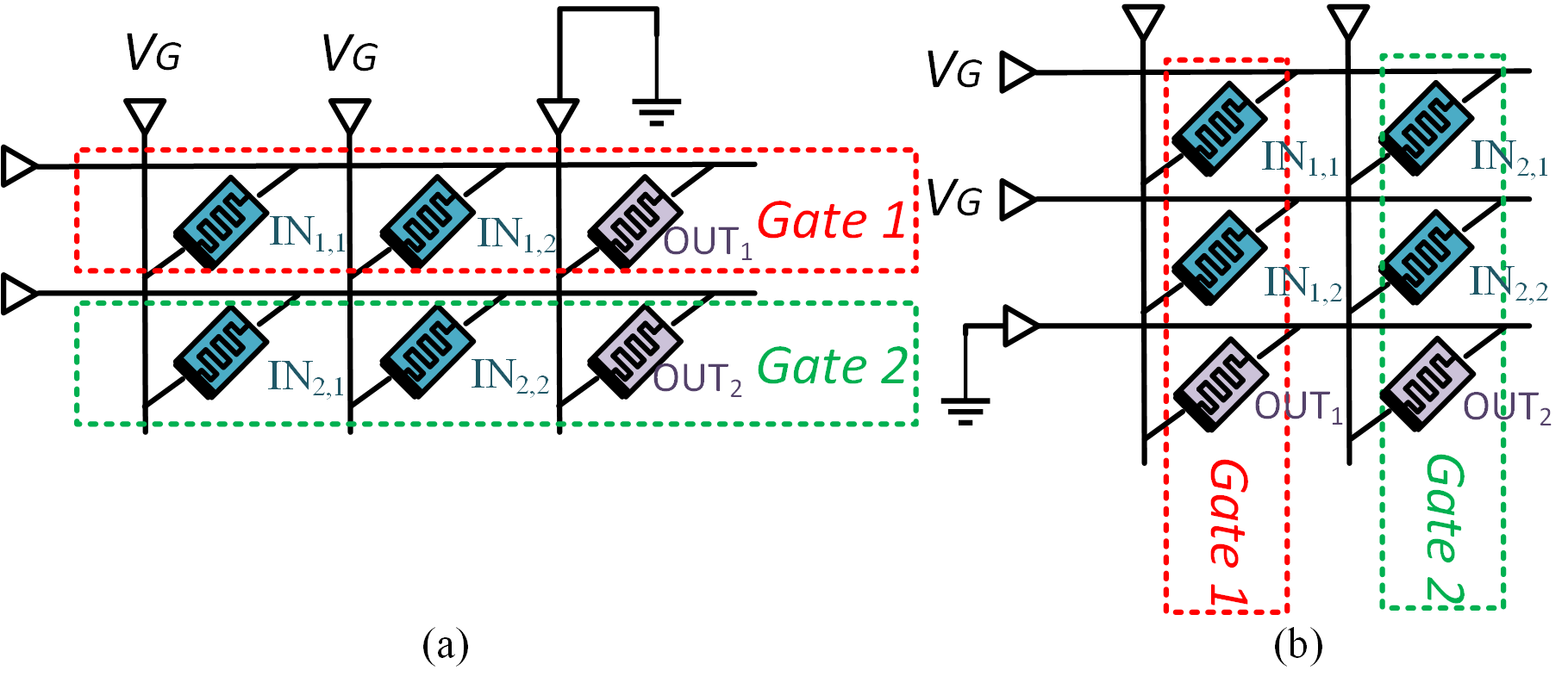
The MAGIC NOR function is performed by applying a single operating voltage () to the input memristor(s) to initialize the output memristor to logic 0 (high resistance value). The state of the output memristor (which is also considered as a memory cell) changes pursuant to the logical states of the input memristor(s). The NOT function is realized as a single-input NOR function. The spatial requirement for a MAGIC gate is that its input(s) and output must be located on the same row, or in the same column of the memristor array. Furthermore, to execute multiple row-wise (or column-wise) MAGIC gates in parallel, their input and output memristors should be aligned along the same set of columns (rows). Fig. 1 depicts crossbar configurations for in-memory execution of two row-wise and two column-wise MAGIC NOR gates in parallel. This figure shows the advantages of MAGIC operation such as the separation between the input(s) and output memristors, the need for only a single , absence of additional peripheral elements, and the ability to perform multiple operations in parallel (Kvatinsky et al., 2014a). Since NOR is a complete logic function, a MAGIC NOR gate is sufficient for the execution of any logic operation within the MCA.
2.1.3. Supergate-Aided Synthesis and SoP-to-NoN Translation
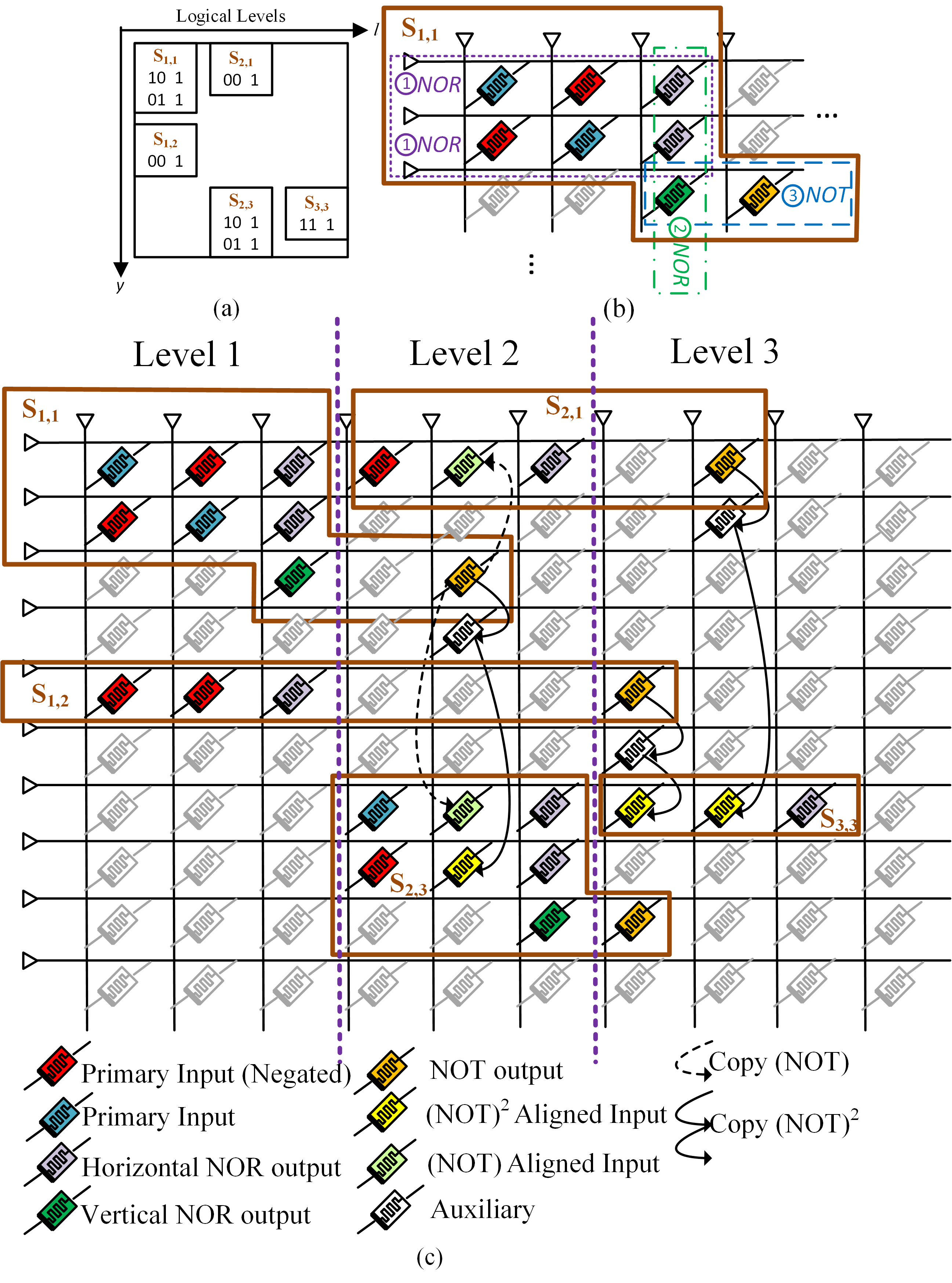
Tenace et al. (Tenace et al., 2019) proposed to use -input LUTs for mapping the subgraphs of an AIG subject graph to the MCA. In their approach, these LUTs are subsequently transformed to NOR-of-NORs (NoN) supergates and implemented on the MCA. Any single-output Boolean function represented by a Sum of Products (SOP) associated with a single LUT can be translated to NoN following these three steps: 1) negating all primary inputs, 2) replacing all AND and OR operations ( and ) with NOR operations. (), and 3) negating the result. The crossbar mapping scheme proposed in (Tenace et al., 2019) for these supergates is a tile-based mapping, where each tile contains a supergate and is expressed by two indices and representing the column and row coordinates of that tile, adhering to some spatial rules. All supergates from one logic level are placed in one column and sorted by their size (i.e., the number of their LUT terms). The mapping scheme in (Tenace et al., 2019) also imposes a constraint that a supergate in position must be smaller in size compared to the supergate placed in tile.
An example of the tile-based mapping for a single-bit full adder is depicted in Fig. 2 (a). An output of a supergate can be generated as a sequence of three MAGIC functions as suggested in Fig. 2 (b). To cascade supergates, alignment copy operations are performed to satisfy the spatial constraints of MAGIC gates. Depending on the polarity of input/output signals, the data alignment copy operations are either NOT copies, or (NOT)2 copies (see Fig. 2 (c)). (NOT)2 copy represent two consecutive NOT copies which use one extra auxiliary memristor for the intermediate signal.
A major challenge of prior work including and (Tenace et al., 2019) and (Thangkhiew and Datta, 2018) is the large computational latency due to alignment copy operations. For instance, main logic operations in Fig. 2 takes only five cycles while alignment copy operations takes 12 cycles. HIPE-MAGIC tackles this challenge by devising a mapping scheme that can further reduce operational computation by overlapping input/output signals as well as sharing alignment copy operations leveraging heuristic placements.
2.2. Motivational Example for MCA-Driven Optimization
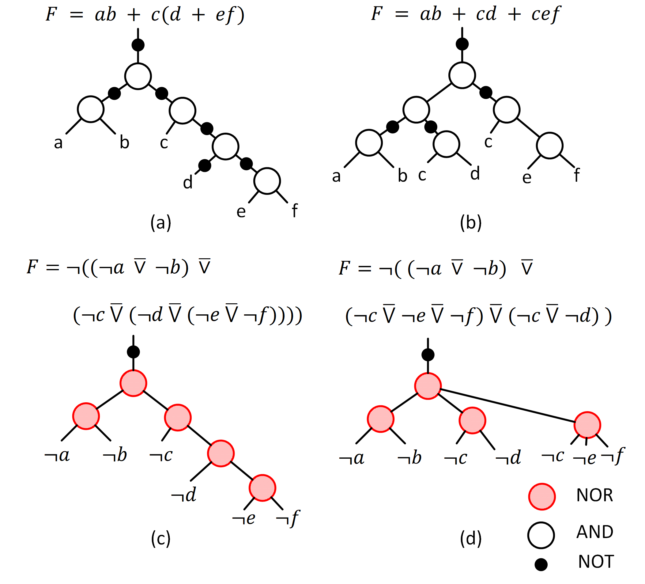
Previous work on optimizing synthesis flow for CMOS illustrate the effect of the balancing operation that reduces the logic depth of a combinational circuit on reducing its delay. In (Mishchenko et al., 2011), Michenko et al. proposed AND balancing and SOP balancing algorithms for the delay optimization. AND-balancing of an AIG is a well-known fast transformation that reduces the number of AIG levels. Pasandi and Pedram (Pasandi and Pedram, 2019) also presented balanced factorization and rewriting algorithms by considering an imbalance factor when calculating the value of a potential factorization. Their results show the importance of the AIG balancing operation in minimizing the delay.
To perform the SOP balancing, a small AIG (e.g., an AIG that depends on say 10 or fewer inputs) is converted into a SOP. Next, the SOP balancing applies AND-balancing to each product and subsequently to the sum operation. Fig. 3 illustrates the SOP-balancing technique on a small AIG (inspired by (Mishchenko et al., 2011)), and how this can be translated into delay optimization of the logic implementation of MAGIC NORs. The total computational cycles needed for implementing this function on the memristive crossbar (e.g., number of logic levels) is reduced from 5 in Fig. 3 (c) to 3 in Fig. 3 (d). This example motivates us to leverage balancing operations, which can lead to improvements for MCA-based PIM by enabling more operations to be performed in parallel.
3. HIPE-MAGIC’s flow
HIPE-MAGIC’s flow is divided into two main steps:
-
•
Logic Synthesis: The input is an arbitrary logic function, and the output is a netlist comprising optimized mapped LUT representation of the input function.
-
•
MCA Mapping: The input is a netlist of synthesized LUTs, and the output is the placement of each supergate within the 2D memristive crossbar array along with a schedule of the sequence of operations.
3.1. Technology-aware Logic Synthesis
Logic synthesis for enabling PIM is a crucial step in the MCA design flow with a significant impact on the total area and performance. The underlying 2D grid in MCAs offers the opportunity for concurrently performing many logic operations in each logic level. This opportunity should be considered during the logic synthesis flow. Similar to prior work, we utilize the ABC tool (Brayton and Mishchenko, 2010), but with the addition of balancing operations. ABC receives an arbitrary logic function, and generates a netlist of optimized LUTs while minimizing the number of gates and logic levels. HIPE-MAGIC runs balancing operations in two phases within the ABC tool:
-
(1)
Technology-independent phase: on the AIG itself (i.e., before mapping the Boolean function to LUTs).
-
(2)
Technology-dependent phase: on the priority cuts (i.e., during the LUT mapping process).
Technology-independent Phase: We have added balanced factorization and rewriting algorithms (Pasandi and Pedram, 2019) as commands to ABC (Brayton and Mishchenko, 2010). These commands tend to reduce the size of the AIG representing the input logic network, and also introduce more parallelism in the AIG by utilizing the balancing operations. We have used the following optimization scripts: {blnc_syn2, resyn, resyn2, resyn2rs, compress2rs} where blnc_syn2 is a set of optimization commands, which is interleaved with balanced rewriting and factorization commands together with the AND balancing command of ABC. The other commands are heuristics methods, provided by the ABC synthesis to further optimize the AIG network.
Technology-dependent Phase: In general, AND-balancing, balanced factorization, and rewriting algorithms are limited to AIG and AND gates, while SOP-balancing can look at larger functions (i.e., the priority-cuts which are used for the -input LUT mapper in ABC (Brayton and Mishchenko, 2010), where denotes the number of LUT inputs). Therefore, SOP-balancing can be applied during the LUT mapping to reduce delay in many cases. However, it is impossible to apply SOP-balancing algorithms to each of the AIG nodes since large design can have millions of AIG nodes. For this purpose, a large AIG is divided into parts (using cutlines), and the SOP-balancing operation is carried out for each of the cuts (for an example, see Fig. 3).
The SOP-balancing operation is implemented in ABC, and called through the priority-cut based mapper if command. We called our optimization script TechDepOpt, which performs the technology-dependent synthesis targeting MCA. The sequence of ABC commands are: st; if -K k; (st; dch; if -K k222The number of rounds of running the sequence of the commands in parenthesis. ; st; if -g -C c -K l; (st; dch; if -K k; st; dch; if -K k -S s. In the TechDepOpt, -g enables SOP-balancing for the cut evaluation and c is the number of l-input cuts computed at each node in the subject graph. dch performs the AIG-based synthesis with a repeated sequence of technology-independent optimizations on different structural choices (which are functionally equivalent networks obtained by running AIG rewriting scripts on the current network), and st transforms the network back to the AIG form. To ensure that the delay after mapping into k-LUT can be reduced, the cut size for SOP-balancing operation (l in ”if -g -C c -K l”) is set to a number larger than the cut size for the final mapping command (k in ”if -K k -S s”). Using a larger cut size for SOP balancing operation can potentially result in better delay optimization.
3.2. Technology Mapping
The method presented in (Tenace et al., 2019), for mapping a netlist of supergates to the MCA, tends to limit the potential performance gain that can be obtained by the parallelization potential offered by the supergates. It also introduces a number of redundant operations, according to how it employs the SOP-to-NoN translation, which can be avoided. Furthermore, to make better use of the 2D crossbar grid, the area-efficiency of mapped gates, associated with how densly memristors used for logic computations are placed next to each other in rows and columns, is preferable. However, the mapping rules presented in (Tenace et al., 2019) may result in a sparse mapping of a netlist (e.g., see Fig. 2), although in fact a denser and more area-efficient mapping may be possible. In addition, the overhead associated with the data alignment copies can be alleviated by reusing auxiliary memristors. Based on above observations, certain refinements and mapping operations are used as shown in Algorithm 1 and elaborated on below.
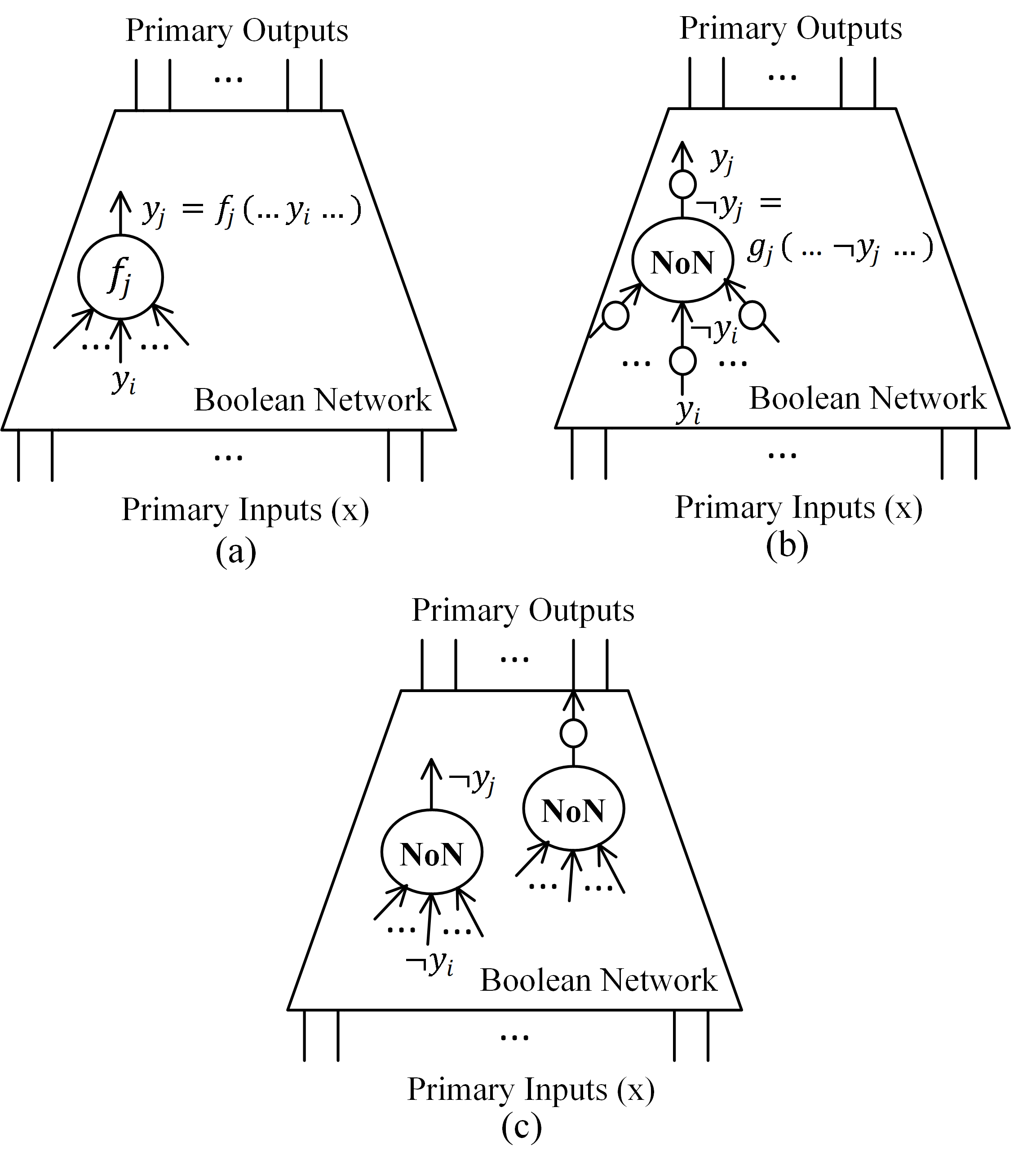
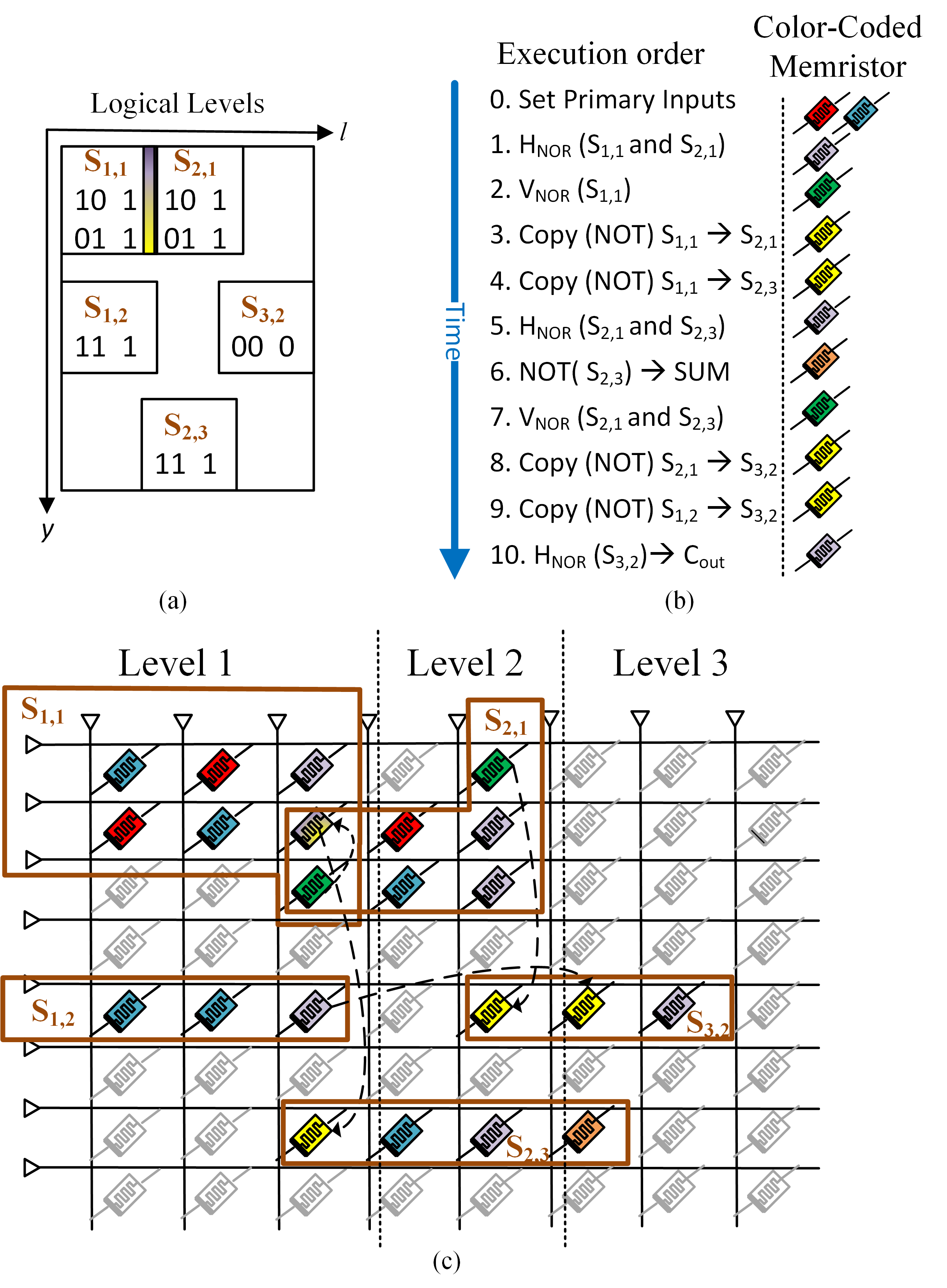
MCA-Driven SOP-to-NoN Translation: For each pair of cascaded LUTs, we merge the third step of the SoP-to-NoN mapping of the second LUT, cf. Section 2.1.3 above, with the first step of the SoP-to-NoN mapping of the first LUT (this is done as part of Map_SOP_to_NoN() function in Algorithm 1). For instance, assume a Boolean network which is a graph of connected blocks (e.g., nodes, LUTs). Here, the individual component blocks are 2-level Boolean functions in the SOP form, which can be represented by where denotes the node’s output variable and and denote node’s input variables, respectively (see Fig. 4 (a)). There exists an edge if depends explicitly on ; differently worded, there is a connection between the node and the node. The SOP-to-NoN translation imposes that each supergate (e.g., the node that is created after translation) depends on negated value of its input nodes, as shown in Fig. 4 (b) where . Therefore, is calculated by performing a NOT function on which is the node variable of . This NOT function is equivalent to the last step in the translation of the SOP representation of into the NoN representation. Eliminating the two NOT functions on an edge between two cascaded nodes (see Fig. 4 (c)) reduces the number of operations required for implementing the target Boolean network. In other words, for each supergate (except for the ones that produce the primary outputs), we discard the third operation (e.g., the NOT function in Fig. 2 (b)).
Placement of Supergates: The spatial rules for the mapping procedure mentioned in Section 2.1.3, rely on the intuition that as the logic level increases, the supergate size decreases. However, this intuition does not always hold true. For instance, in the mapping of the one-bit full adder depicted in Fig. 2, and will be pushed down in each column (logic level) following the spatial rules although they can be placed higher up in those columns. These replacements increase the area-efficiency of the mapped supergates, which thus make better use of the underlying 2D grid of memristors.
We first sort the supergates in each logic level () in the decreasing order of their size ((Sort_Supergates() function in Algorithm 1)). To take advantage of the underlying 2D grid, we alter the direction of the vertical NOR in supergates for consecutive columns (this is done in Flip_Supergates() function in Algorithm 1). Next, we place the supergates of first logic level () in the first column following the sorting order. For subsequent columns, we go through the sorted supergates in each level and place each supergate in the first available vertical position () in the column where the output of the supergate in the same and level would be one of the inputs of the supergate in level . We also align the supergate in level with the one in level in a way that the memristor corresponding to the output of the supergate in level is shared with the corresponding input of the supergate in level in its first row. In this way, one data alignment copy is saved for each pair of cascading supergates in the same . At the end, for those supergates in level that were not placed in column as a result of the described process, we place them in the decreasing order of their size in the first available in column (this is done in Place_Supergates() function in Algorithm 1 for each column ).
Using this placement scheme, supergates corresponding to and in Fig. 2 (a) are pushed up in their respective columns (i.e., and in Fig. 5 (a), respectively), which improves the area efficiency. Furthermore, the output memristor of is shared as one of inputs of , as they are cascaded supergates in the same y position, which saves one data alignment copy. Note that the assumption for the underlying MCA dimension in this work is , which is a typical value range for dimensions of an MCA based on (Korgaonkar et al., 2019). This means that the total number of terms within supergates of one logical level must not exceed 1024, which was the case in our experiments.
Resource Sharing for Data Alignment Copies: When the output of a supergate should be aligned to any row(s) of cascaded supergates in the next logic level, two NOT copies are used for each alignment with the aid of one auxiliary memristor. However, by sharing the auxiliary memristor for alignment copies that must be carried out for the output of the supergate and doing the second NOT for each alignment from that memristor (represented by Share_Align_Memristors() function in Algorithm 1), we reduce both latency and memristor count. In Fig. 5, we see an example for the advantage of resource sharing for data alignment copies, as we reuse one of input memristors of for transferring output of to .
4. Experimental Results
We used ISCAS’85 and IWLS’93 benchmark suites for our performance evaluation. A Python script runs ABC by leveraging optimizing scripts during synthesis and varying values { = 2,3,7,10}. Next, technology mapping is done according to the mapping scheme presented in Section 3.2. Lastly, the design spaces for each benchmark (associated with different values of ) is explored through a Pareto analysis and the best solution for each benchmark in terms of the area-latency trade-off is determined as the solution associated with the HIPE-MAGIC. Note that the real-time control of the MCA implementing the logic function (i.e., a sequencer which activates rows and columns of the MCA) is not considered. Also, it is worth mentioning that considering the electrical conditions of MCA such as current sneak path is out of the scope of this paper.
| Benchmark | Circuit | HIPE-MAGIC | Tenace et al. (Tenace et al., 2019) | Thangkhiew and Datta (Thangkhiew and Datta, 2018) | |||||||
| Cycles | Mems | Cycles | Mems | Speedup | Area-Saving | Cycles | Mems | SpeedUp | Area-Saving | ||
| ISCAS’85 | c432 | 122 | 366 | 156 | 631 | 1.28 | 1.72 | 265 | 372 | 2.17 | 1.02 |
| c499 | 253 | 836 | 420 | 1399 | 1.66 | 1.67 | 935 | 1085 | 3.70 | 1.30 | |
| c880 | 219 | 862 | 482 | 1113 | 2.20 | 1.29 | 750 | 886 | 3.42 | 1.03 | |
| c1355 | 253 | 836 | 554 | 1182 | 2.19 | 1.41 | 938 | 1076 | 3.71 | 1.29 | |
| c1908 | 313 | 809 | 627 | 1095 | 2.00 | 1.35 | 970 | 1061 | 3.10 | 1.31 | |
| c2670 | 332 | 1462 | 643 | 1249 | 1.94 | 0.85 | 1401 | 1915 | 4.22 | 1.31 | |
| c3540 | 758 | 2544 | 1566 | 3261 | 2.06 | 1.29 | 2418 | 2663 | 3.19 | 1.05 | |
| c5315 | 1043 | 3556 | 1754 | 2937 | 1.68 | 0.83 | 3239 | 3795 | 3.11 | 1.07 | |
| c6288 | 2429 | 5141 | 4069 | 6067 | 1.67 | 1.19 | 5007 | 5344 | 2.06 | 1.04 | |
| c7552 | 1510 | 3507 | 2565 | 4003 | 1.69 | 1.14 | 3824 | 4415 | 2.53 | 1.26 | |
| Average | 723.2 | 1991.9 | 1283.6 | 2293.7 | 1.84 | 1.27 | 1974.7 | 2261.2 | 3.12 | 1.17 | |
| IWLS’98 | 9sym | 99 | 154 | 160 | 1026 | 1.61 | 1.78 | 552 | 594 | 5.57 | 1.03 |
| apex5 | 371 | 1910 | 777 | 2223 | 2.09 | 1.16 | 1966 | 2319 | 5.30 | 1.21 | |
| clip | 54 | 310 | 135 | 451 | 2.50 | 1.45 | 239 | 261 | 4.42 | 0.84 | |
| duke2 | 263 | 1037 | 300 | 1632 | 1.14 | 1.57 | 1261 | 1342 | 4.80 | 1.29 | |
| inc | 21 | 296 | 55 | 280 | 2.62 | 0.95 | 264 | 282 | 12.57 | 0.95 | |
| misex3c | 183 | 1585 | 518 | 2551 | 2.83 | 1.61 | 2976 | 3094 | 16.26 | 1.95 | |
| rd73 | 27 | 232 | 150 | 379 | 5.55 | 1.63 | 262 | 280 | 9.70 | 1.21 | |
| sao2 | 54 | 344 | 79 | 559 | 1.46 | 1.62 | 309 | 331 | 5.72 | 0.96 | |
| vg2 | 27 | 172 | 55 | 280 | 2.04 | 1.63 | 289 | 345 | 10.70 | 2.01 | |
| Average | 122.11 | 671.11 | 247.67 | 1042.33 | 2.43 | 2.03 | 902 | 983.11 | 8.34 | 1.59 | |
4.1. Operation Complexity and Area Comparison
We evaluate the proposed approach by calculating the numbers of compute cycles and memristors required for each benchmark using the proposed synthesis and mapping flow. Area and latency improvements of the HIPE-MAGIC with respect to some of the state-of-the-art prior work are reported in TABLE 1. We compare HIPE-MAGIC with the mapping approach presented in (Tenace et al., 2019), and the work in (Thangkhiew and Datta, 2018) which presents a mapping procedure for a netlist consisting of MAGIC NOR/NOT gates based on a simulated annealing algorithm to minimize the number of computational cycles. For each MCA-based implementation, we compare the number of cycles required to generate all primary outputs (Cycles in TABLE 1), and the number of memristors required to implement the synthesized netlist (Mems in TABLE 1).
Results confirm that proposed optimization scripts leveraging the balancing operations reduce the latency by offering more opportunities for executing multiple supergates of a logic level concurrently, while simultaneously reducing the number of logic levels. However, the proposed scripts may add some redundancies in terms of logic and/or supergates to keep the logic level balanced, which may introduce area overheads. A particular mention is required for c2670 and c5315 where HIPE-MAGIC has a small area overhead compared to (Tenace et al., 2019). It is worth mentioning that a favorable trade-off between speed and area can be obtained in HIPE-MAGIC by setting a different value of k. In addition, the dedicated proposed mapping flow compensates the potential area overhead due to redundancy introduced by supergates, and also reduces the latency mainly by sharing resources for data alignment copies. In particular, HIPE-MAGIC outperforms (Tenace et al., 2019) in terms of the latency by an average of 2.11x improvement across both benchmark suites, while using 1.37x fewer memristors. Concerning the meta-heuristic mapping solution presented in (Thangkhiew and Datta, 2018), HIPE-MAGIC is 3.12x (8.34x) faster, requiring 1.17x (1.59x) fewer memristors for ISCAS’85 (IWLS’98) benchmarks.
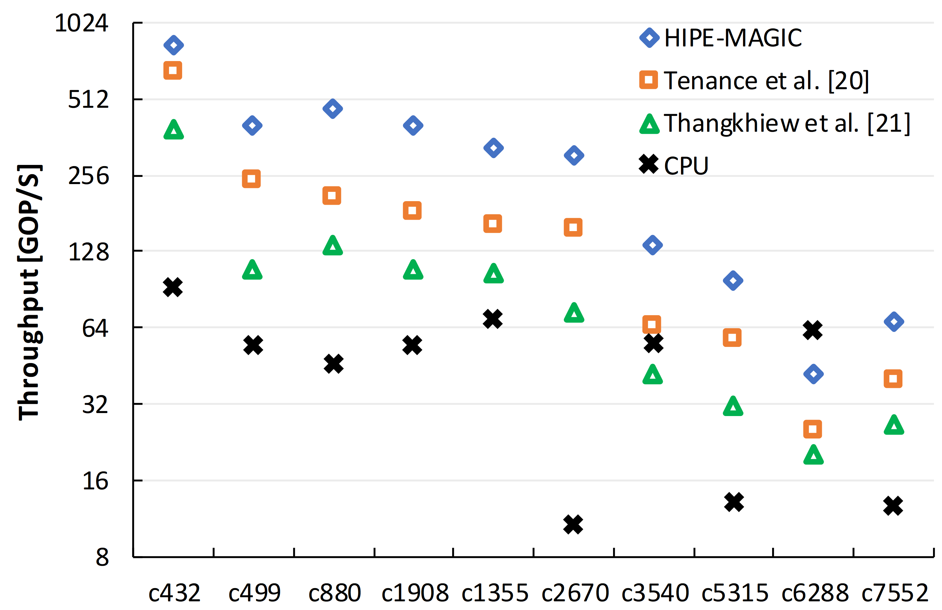
4.2. Analytical Comparison - PIM vs. CPU
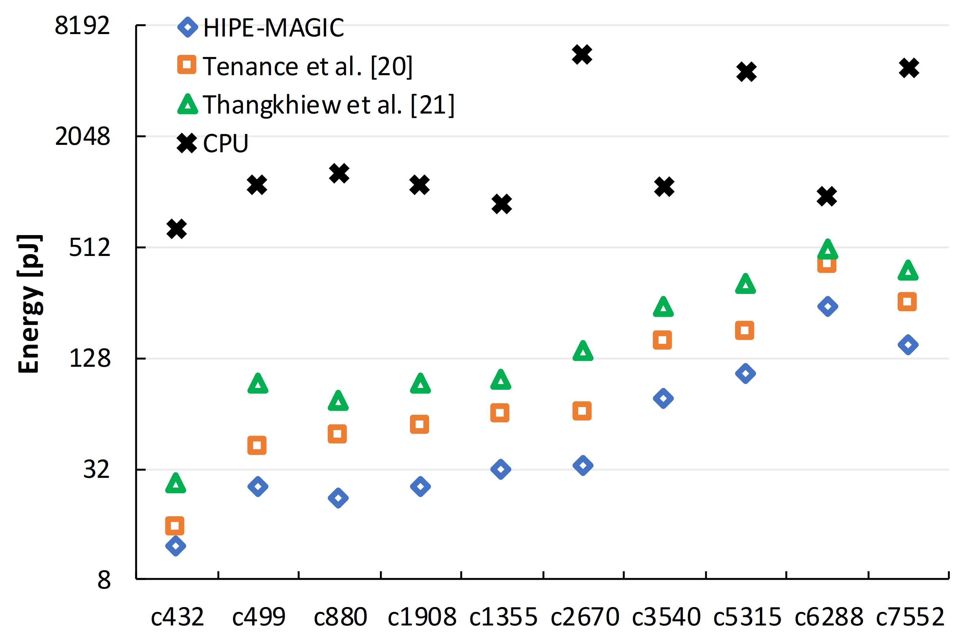
We analyze and quantify the strengths and weaknesses of our PIM realization over conventional CPU and other PIM solutions from [17] and [14]. For our comparison, we employ a parameterized analytical modeling tool presented in (Korgaonkar et al., 2019) (and referred to as Bitlet), which evaluates the affinity of workloads to PIM versus CPU computing according to some PIM- and CPU-related parameters. PIM computations in the Bitlet model are limited mainly by operation complexity and data alignment costs, i.e., the number of PIM cycles in Table 1. On the other hand, for CPU computing, Bitlet ignores the cost associated with computations and data movements done within the CPU itself (which is indeed in the favor of CPU computing for our comparison), and the CPU throughput is thus mainly limited by its external memory bandwidth utilization, i.e., the cost associated with the number of data bits transferred between the CPU and memory (Korgaonkar et al., 2019). Bitlet uses technology parameters for a 28nm node from (O’Connor et al., 2017) for the memory model in CPU and bases its model of memristor on (Lanza et al., 2019).
Using the Bitlet model, Fig. 6 (a) shows a comparison in terms of achieved throughput between PIM solutions (including HIPE-MAGIC) and CPU computing. Notice that the PIM does not achieve any improvements in terms of throughput for c6288, because this circuit is an array multiplier with a relatively large number of PIM cycles. Furthermore, the comparison between PIM and CPU with respect to c2670, which has a relatively large number of input/output lines (which affects the CPU throughput adversely), demonstrates that PIM can greatly alleviate the overheads associated with data transfers from/to the main memory.
Comparing the energy obtained using the Bitlet model, CPU energy consumption is higher than that of PIM solutions over all the studied benchmarks (see Fig. 6 (b)). For the CPU, energy consumption is associated with the number of transferred bits and energy per bit transfer, while operation complexity and PIM energy per each operation determine the energy consumption for PIM solutions. As the number of PIM cycles increase, the relative energy efficiency of PIM decreases (e.g., c6288).
These results demonstrate once again that PIM-based solutions are beneficial if much of the latency and energy consumption associated with a target application is due to data transfers between memory and the computing fabric. There are many such interesting applications including for example big data analysis, neural network based inference, and so on.
5. Conclusion
In this paper, we presented a technology-aware synthesis approach along with a heuristic mapping framework. Results show that the HIPE-MAGIC achieves promising results compared to state-of-the-art work and the conventional CPU computing. As data alignment copy operations contribute to significant number of cycles for implementing a logic function, restricting the number of fan-outs of LUT nodes during logic synthesis can be a promising future work.
References
- (1)
- Balasubramonian et al. (2014) Rajeev Balasubramonian et al. 2014. Near-data processing: Insights from a MICRO-46 workshop. IEEE Micro (2014).
- Ben-Hur et al. (2019) R. Ben-Hur et al. 2019. SIMPLER MAGIC: Synthesis and Mapping of In-Memory Logic Executed in a Single Row to Improve Throughput. IEEE Trans. CAD Integr. Circuits Syst. (2019). https://doi.org/10.1109/TCAD.2019.2931188
- Borghetti et al. (2010) Julien Borghetti et al. 2010. ’Memristive’ switches enable ’stateful’ logic operations via material implication. Nature (2010).
- Brayton and Mishchenko (2010) Robert Brayton and Alan Mishchenko. 2010. ABC: An Academic Industrial-Strength Verification Tool. In Computer Aided Verification. Springer.
- Chakraborti et al. (2014) S. Chakraborti et al. 2014. BDD based synthesis of Boolean functions using memristors. In IDT. https://doi.org/10.1109/IDT.2014.7038601
- Fujiki et al. (2018) Daichi Fujiki, Scott Mahlke, and Reetuparna Das. 2018. In-memory data parallel processor. In ACM SIGPLAN Notices, Vol. 53. ACM, 1–14.
- Imani et al. (2019) Mohsen Imani et al. 2019. FloatPIM: In-memory Acceleration of Deep Neural Network Training with High Precision. In ISCA.
- Korgaonkar et al. (2019) Kunal Korgaonkar et al. 2019. The Bitlet Model: Defining a Litmus Test for the Bitwise Processing-in-Memory Paradigm. arXiv preprint arXiv:1910.10234 (2019).
- Kvatinsky et al. (2011) Shahar Kvatinsky et al. 2011. Memristor-based IMPLY logic design procedure. In ICCD.
- Kvatinsky et al. (2014a) S. Kvatinsky et al. 2014a. MAGIC-Memristor-Aided Logic. TCAS-II: Express Briefs (2014). https://doi.org/10.1109/TCSII.2014.2357292
- Kvatinsky et al. (2014b) S. Kvatinsky et al. 2014b. Memristor-Based Material Implication (IMPLY) Logic: Design Principles and Methodologies. IEEE Trans. VLSI Syst. (2014).
- Lanza et al. (2019) Mario Lanza et al. 2019. Recommended methods to study resistive switching devices. 5, 1 (2019), 1800143.
- Lu et al. (2011) W. Lu et al. 2011. Two-terminal resistive switches (memristors) for memory and logic applications. In ASP-DAC.
- Mishchenko et al. (2011) A. Mishchenko et al. 2011. Delay optimization using SOP balancing. In ICCAD.
- O’Connor et al. (2017) M. O’Connor et al. 2017. Fine-Grained DRAM: Energy-Efficient DRAM for Extreme Bandwidth Systems. In MICRO.
- Pasandi and Pedram (2019) Ghasem Pasandi and Massoud Pedram. 2019. Balanced Factorization and Rewriting Algorithms for Synthesizing Single Flux Quantum Logic Circuits. In GLSVLSI. https://doi.org/10.1145/3299874.3317967
- Seshadri et al. (2014) Sudharsan Seshadri, Mark Gahagan, Sundaram Bhaskaran, Trevor Bunker, Arup De, Yanqin Jin, Yang Liu, and Steven Swanson. 2014. Willow: A User-Programmable SSD. In 11th USENIX Symposium on Operating Systems Design and Implementation (OSDI 14). 67–80.
- Seshadri et al. (2017) Vivek Seshadri et al. 2017. Ambit: In-memory accelerator for bulk bitwise operations using commodity DRAM technology. In MICRO.
- Talati et al. (2016) N. Talati et al. 2016. Logic Design Within Memristive Memories Using Memristor-Aided loGIC (MAGIC). IEEE Trans. Nanotechnol. (2016). https://doi.org/10.1109/TNANO.2016.2570248
- Tenace et al. (2019) V. Tenace et al. 2019. SAID: A Supergate-Aided Logic Synthesis Flow for Memristive Crossbars. In DATE. https://doi.org/10.23919/DATE.2019.8714939
- Thangkhiew and Datta (2018) Phrangboklang L. Thangkhiew and Kamalika Datta. 2018. Scalable in-memory mapping of Boolean functions in memristive crossbar array using simulated annealing. Journal of Systems Architecture (2018). https://doi.org/10.1016/j.sysarc.2018.07.002
- Wulf and McKee (1995) Wm A Wulf and Sally A McKee. 1995. Hitting the memory wall: implications of the obvious. ACM SIGARCH computer architecture news (1995).