Large optical tunability from charge density waves in 1T-TaS2 under incoherent illumination
Abstract
Strongly correlated materials possess a complex energy landscape and host many interesting physical phenomena, including charge density waves (CDWs). CDWs have been observed and extensively studied in many materials since their first discovery in 1972. Yet, they present ample opportunities for discovery. Here, we report a large tunability in the optical response of a quasi-2D CDW material, 1T-TaS2, upon incoherent light illumination at room temperature. We show that the observed tunability is a consequence of light-induced rearrangement of CDW stacking across the layers of 1T-TaS2. Our model, based on this hypothesis, agrees reasonably well with experiments suggesting that the interdomain CDW interaction is a vital knob to control the phase of strongly correlated materials.
keywords:
charge density waves, 1T-TaS2, tunable optical properties, stacking structureAPP Rice] Applied Physics Graduate Program, Smalley-Curl Institute, Rice University, Houston, TX 77005, USA ECE Rice] Electrical & Computer Engineering, Rice University, TX 77005, USA \phone+1 (713)-348-2528 \abbreviationsCDW,TMDs
1 Introduction
Light-matter interaction in strongly correlated materials is interesting because light can significantly alter the free energy landscape of strong correlations resulting in many new physical phenomena 1, 2, 3. Optical excitation can tip the balance between various competing forms of order leading to photo-induced metal-to-insulator transitions 4, 5, 6, charge density waves 7, 8, 9, 10, ferromagnetic/antiferromagnetic transitions 11, 12, superconductivity 13, and others 14. Though light-induced changes in the lattice, electrical, and magnetic properties have been extensively studied before, optical properties remain much to be explored. In this work, we study the tunable optical properties of a strongly correlated material, 1T-TaS2, which supports charge density waves (CDWs) at room temperature.
Many chalcogenides and organic compounds support CDWs at low temperatures 15. However, 1T-TaS2, 1T-TaSe2, and a few other lanthanide tellurides support CDWs at room temperature and are interesting for device applications 16, 17, 18, 19, 20. Among them, 1T-TaS2 is the only material that exhibits nearly commensurate CDW (NCCDW) phase at room temperature resulting in a large tunability in its electrical conductivity.
The tunability of electrical properties of 1T-TaS2 is extensively studied in the past. 1T-TaS2 was shown to exhibit nonlinear electrical conductance at room temperature 21, and hysteresis behavior of its electric resistance 22, 23, 24. Also, the CDW phase transition was demonstrated to be sensitive to pressure 25, 26, strain 27, 28, thickness 29, 30, gate voltage 31, 32, 33, and chemical doping 34, 35. However, the optical properties of 1T-TaS2 and its tunability remain unexplored. In this work, we study light-tunable optical properties of 1T-TaS2.
The charge order in 1T-TaS2 manifests as a lattice reorganization where 12 Ta atoms surrounding a central Ta atom move slightly inwards forming a David-star structure (see Fig. 1a). Groups of such David-stars called CDW domains exist in each layer of 1T-TaS2 at room temperature. The relative position or stacking arrangement of such CDW domains across layers has been recently reported to impact the electronic bandstructure of 1T-TaS2 significantly 36, 37, 38, 39. Depending on the stacking, the material can be insulating or metallic along its c-axis. Such drastic dependence of the electronic properties on the CDW stacking configuration is unusual and forms the central theme of this work. Here, we observe a substantial change in the dielectric function of 1T-TaS2 only in the c-axis upon incoherent white light illumination. We attribute the observed changes in the dielectric function to the stacking rearrangement of the CDW domains in 1T-TaS2.
2 Results and discussion
We obtained crystalline 1T-TaS2 thin film samples by mechanical exfoliation, as reported in our previous work 40. The reflectance of a 180 nm thick film measured at three different wavelengths using an objective of 0.85 numerical aperture is shown in Fig. 1b as a function of illumination intensity. The 1T-TaS2 film exhibits an intensity-dependent reflectance even at low illumination intensities of a few mW/cm2. For comparison, the peak intensity of 1.5AM sun is approximately 100 mW/cm2.
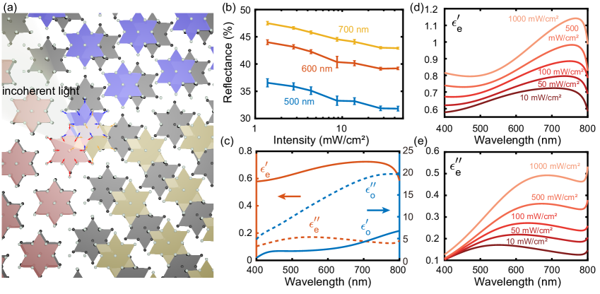
Using a Fourier plane imaging spectrometer, we measure the reflection and transmission spectra of the 1T-TaS2 film at incident angles ranging from 0 to 53∘. From this data, we extract the anisotropic dielectric function of 1T-TaS2 in the visible (see SI). The in-plane and out-of-plane (along c-axis) dielectric functions denoted by and respectively are shown in Fig. 1c for low illumination. 1T-TaS2 is strongly anisotropic and highly absorbing dielectric in the visible.
As we increase the incoherent illumination intensity up to 1000 mW/cm2, the in-plane dielectric function remains the same (see SI), but the out-of-plane dielectric function changes. The real and imaginary parts of the intensity-dependent are as shown in Fig. 1d and e. The real component of out-of-plane epsilon () increases by about 0.4 and the imaginary component () increases by about 0.5 as the incident incoherent light intensity increases from 10 mW/cm2 to 1000 mW/cm2.
The observed light-induced change in c-axis dielectric function could be a result of many possible microscopic phenomena. The low intensity of the white light used in these experiments rule out photothermal effects (see SI). Light-induced free carrier generation could account for the observed change in optical constants only if the lifetime of these carriers is about a millisecond. Such a large lifetime for free carriers is not physical. Additionally, the dielectric constants changing only along c-axis suggests a mechanism that involves interlayer interaction. To further probe the underlying mechanism, we carry out time-resolved measurements.
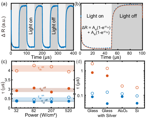
At first, the change in optical properties of 1T-TaS2 with illumination was suspected to arise from free carriers. Hence, a ps-pulsed laser was used to measure time-resolved reflectance (see SI). We observed a s response time and hence ruled out a free carrier mechanism for the change in optical constants. Then, we perform time-resolved measurements with a few kHz to a few 100’s of kHz modulated laser incident on 1T-TaS2 thin films. The measured change in reflectance of the 1T-TaS2 film at 785 nm wavelength is plotted against time in Fig. 2a. A square wave modulates the pump laser at 640 nm wavelength and the pump light-on and light-off regions are shown in Fig. 2. The modulated reflectance signal from the 1T-TaS2 film was repeatable for at least 600 s in ambient air.
The observed change in reflectance () could be fitted well with a sum of two exponential functions, as indicated in Fig. 2b. The two time-constants each for light-on and light-off transients are plotted in Fig. 2c as a function of the peak pump intensity. The time-constants are nearly independent on intensity and suggest that there must be at least two mechanisms behind the observed . Since the smallest laser intensity in Fig. 2 is about an order of magnitude more than that of white light in Fig. 1, photothermal effects could be expected as one of the mechanisms contributing to the in Fig. 2. Many previous studies on 1T-TaS2 have used intense lasers and observed photothermal effects, including phase transition to incommensurate CDW (ICCDW) state 41, 42.
Photothermal effects depend on the thermal conductivity of the substrate. Hence, measuring time-constants for 1T-TaS2 on different substrates could elicit the photothermal effect. Fig. 2d shows the time-constants measured on four different substrates: glass, glass with an 80 nm silver layer, sapphire, and silicon. One of the two time-constants shrinks with increasing thermal conductivity of the substrate for both light-on and light-off cases. We attribute this time-constant to the photothermal phenomenon. The difference between the photothermal time-constants for light-on and light-off cases could arise from the temperature-dependent thermal conductivity of 1T-TaS2. Note that for sapphire and silicon substrates are small and comparable to the other time-constant. Hence, its extraction was not uniquely possible.
While the photothermal time-constant shows a strong substrate dependence, the other does not. This other time-constant could be related to the CDW phenomenon because CDWs in 1T-TaS2 typically exhibit a response time of 100’s of ns. This underlying CDW phenomenon should be common to both measurements, under white light (Fig. 1) and laser (Fig. 2), and account for the observed light-induced change in c-axis dielectric function.
Since dielectric function changes only along the c-axis, light could be rearranging CDW domains in the layers of 1T-TaS2 resulting in a change in CDW stacking across layers. Recently, CDW stacking has been shown to strongly influence the band structure of 1T-TaS2, especially in the A direction 36. Thus, we hypothesize that the change in the c-axis dielectric function of 1T-TaS2 originates from the rearrangement of CDW stacking across layers.
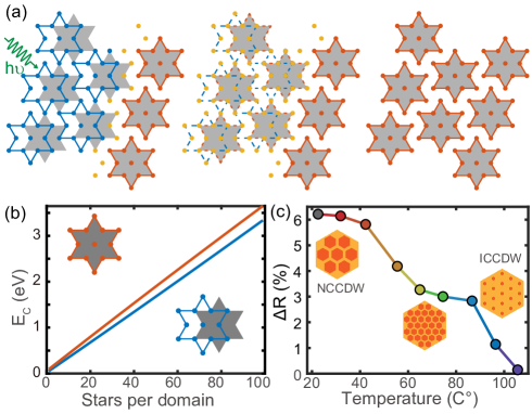
The proposed mechanism of light-induced rearrangement of CDW stacking is depicted in the schematic of Fig. 3a. At first, the absorption of a visible light photon breaks a CDW domain. Subsequently, new domains with different stacking configurations appear. The schematic identifies the most likely stacking configurations with and without light. In the dark, the Coulomb repulsion between the CDW domains energetically favors the center-to-shoulder stacking configuration. Upon illumination, some David stars stack on top of each other in the center-to-center configuration. The calculated interlayer Coulomb repulsion energies for the two stacking configurations are shown in Fig. 3b as a function of domain size (See SI for further details of calculations). At room temperature, a typical domain contains a few tens of stars 43, and hence the energy difference between the two stacking types is about 150 meV. As the temperature increases, the domain size shrinks and reduces the energy difference between the two stacking configurations. Thus, increasing temperature makes both stacking configurations more equally probable. Therefore, the tunability of the c-axis dielectric function should diminish with increasing temperature and eventually vanish in the ICCDW phase. Fig. 3c plots the temperature-dependent measured at 700 nm wavelength with a low intensity incoherent optical pump. The tunability drops with increasing temperature and vanishes in the ICCDW phase as expected.
The proposed mechanism of CDW stacking rearrangement involves at least three steps: setting electrons and phonons of a domain free by optical absorption, formation of a new domain in center-to-center stacking configuration (stacking ) and relaxation to ground state or center-to-shoulder stacking configuration (stacking ). The three processes together could be modeled as a three-level system shown in Fig. 4a. The relaxation times for the formation of a new domain in stacking configurations and are and respectively. The relaxation time for a transition from stacking to is . should correspond to the light-off relaxation time from our time-resolved measurements (). and do not involve any stacking change and hence should be much smaller than . Previous works report and in the order of 500 ps around 200 K, and show an increasing trend with higher temperature 41, 7. Therefore, we expect and to be a few nanoseconds at room temperature.
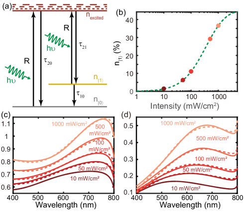
Using the three-level model, the steady-state fractions of CDW domains in the two stacking configurations could be computed as a function of illumination intensity. Fig. 4b plots the fraction of CDW domains in stacking () as a function of incident light intensity. Note that the equilibrium value of is approximated to zero because the energy gap between the two staking levels is more than at room temperature (previous discussion about Fig. 3b). From the rate equations, at steady-state, . In the limit, and , for . We set 3 ns and 0.38 s. For the intensities used in this work, and thus the maximum value of is close to 50%. Also, as a function of is determined by only one parameter, . Since, our time-resolved experiments measured , we expect the prediction of Fig. 4b to be quantitative.
The electronic bandstructure of 1T-TaS2 along has been predicted to depend on the CDW stacking order 36. Hence, we associate each stacking configuration to a unique dielectric function along the c-axis. We calculate the c-axis dielectric function for any intensity of incident light by using the population fraction information from Fig. 4b in Maxwell-Garnet effective medium equation 44. The lowest intensity of incoherent light used in Fig. 1 corresponds to 1% and hence may be considered as the c-axis dielectric function of ground state stacking. Since this ground state is a two-Lorentzian curve, we expect the corresponding to stacking is also a two-Lorentzian curve. The parameters of the two Lorentzian oscillators corresponding to stacking are obtained by fitting the effective permittivity from the Maxwell-Garnett equation to the measured dielectric function for the highest intensity, 1000 mW/cm2. The value of for this intensity is taken from Fig. 4b. The corresponding to the intermediate three intensities are calculated from the Maxwell-Garnett equation incorporating appropriate values of shown in Fig. 4b. The experimental and calculated c-axis dielectric functions for various light intensities are plotted in Fig. 4c, and Fig. 4c. The effective medium calculations agree well with experiments providing quantitative evidence for our hypothesis of light-induced CDW stacking rearrangement in 1T-TaS2.
In conclusion, we discovered a new optical phenomenon in 1T-TaS2. Our work showed that low-intensity white light illumination could change the c-axis permittivity of 1T-TaS2 by unity-order. Time-resolved measurements showed that the speed of change is a few MHz. We hypothesized that the stacking of CDW domains across layers could rearrange with illumination and thereby lead to a change in c-axis optical constants. Our modeling results agreed well with experimental measurements upholding our hypothesis. This discovery proves that the electronic bandstructure depends on the CDW stacking order, and the stacking order may be controlled by light. Our work shows that stacking order is a new dimension in the phase diagram of strongly correlated materials and enriches opportunities for discovery. This work could lead to further development of low-power and fast-tunable optical materials and potentially revolutionize future imaging, display, and sensing applications.
The authors thank Bharadwaj group at Rice University for their help in optical characterization, and also thank all Naik group members for useful discussion and help with preparing this manuscript.
The supporting information is available free of charge via the Internet at http://pubs.acs.org.
-
•
SI: Methods; Ordinary and extraordinary dielectric functions; Dielectric function extraction; Time-resolved measurements using an ultrafast laser; Photothermal effect; Coulomb energy.
References
- Matsunaga et al. 2014 Matsunaga, R.; Tsuji, N.; Fujita, H.; Sugioka, A.; Makise, K.; Uzawa, Y.; Terai, H.; Wang, Z.; Aoki, H.; Shimano, R. Light-induced collective pseudospin precession resonating with Higgs mode in a superconductor. Science 2014, 345, 1145–1149
- Sie et al. 2019 Sie, E. J.; Nyby, C. M.; Pemmaraju, C.; Park, S. J.; Shen, X.; Yang, J.; Hoffmann, M. C.; Ofori-Okai, B.; Li, R.; Reid, A. H., et al. An ultrafast symmetry switch in a Weyl semimetal. Nature 2019, 565, 61–66
- Tao et al. 2016 Tao, Z.; Zhou, F.; Han, T.-R. T.; Torres, D.; Wang, T.; Sepulveda, N.; Chang, K.; Young, M.; Lunt, R. R.; Ruan, C.-Y. The nature of photoinduced phase transition and metastable states in Vanadium dioxide. Sci. Rep. 2016, 6, 1–10
- Hu et al. 2016 Hu, W.; Catalano, S.; Gibert, M.; Triscone, J.-M.; Cavalleri, A. Broadband terahertz spectroscopy of the insulator-metal transition driven by coherent lattice deformation at the SmNiO3/LaAlO3 interface. Phys. Rev. B 2016, 93, 161107
- Lourembam et al. 2016 Lourembam, J.; Srivastava, A.; Cheng, L.; Venkatesan, T.; Chia, E. E., et al. Evidence for Photoinduced Insulator-to-Metal transition in B-phase Vanadium dioxide. Sci. Rep. 2016, 6, 25538
- Perfetti et al. 2006 Perfetti, L.; Loukakos, P.; Lisowski, M.; Bovensiepen, U.; Berger, H.; Biermann, S.; Cornaglia, P.; Georges, A.; Wolf, M. Time Evolution of the Electronic Structure of 1T- TaS2 through the Insulator-Metal Transition. Phys. Rev. Lett. 2006, 97, 067402
- Vaskivskyi et al. 2015 Vaskivskyi, I.; Gospodaric, J.; Brazovskii, S.; Svetin, D.; Sutar, P.; Goreshnik, E.; Mihailovic, I. A.; Mertelj, T.; Mihailovic, D. Controlling the metal-to-insulator relaxation of the metastable hidden quantum state in 1T-TaS2. Sci. Adv. 2015, 1, e1500168
- Frigge et al. 2017 Frigge, T.; Hafke, B.; Witte, T.; Krenzer, B.; Streubühr, C.; Syed, A. S.; Trontl, V. M.; Avigo, I.; Zhou, P.; Ligges, M., et al. Optically excited structural transition in atomic wires on surfaces at the quantum limit. Nature 2017, 544, 207–211
- Perfetti et al. 2008 Perfetti, L.; Loukakos, P. A.; Lisowski, M.; Bovensiepen, U.; Wolf, M.; Berger, H.; Biermann, S.; Georges, A. Femtosecond dynamics of electronic states in the Mott insulator 1T-TaS2 by time resolved photoelectron spectroscopy. New J. Phys. 2008, 10, 053019
- Stahl et al. 2020 Stahl, Q.; Kusch, M.; Heinsch, F.; Garbarino, G.; Kretzschmar, N.; Hanff, K.; Rossnagel, K.; Geck, J.; Ritschelm, T. Collapse of layer dimerization in the photo-induced hidden state of 1T-TaS2. Nat. Commun. 2020, 11, 1247
- Eggebrecht et al. 2017 Eggebrecht, T.; Möller, M.; Gatzmann, J. G.; da Silva, N. R.; Feist, A.; Martens, U.; Ulrichs, H.; Münzenberg, M.; Ropers, C.; Schäfer, S. Light-induced metastable magnetic texture uncovered by in situ Lorentz microscopy. Phys. Rev. Lett. 2017, 118, 097203
- Stupakiewicz et al. 2017 Stupakiewicz, A.; Szerenos, K.; Afanasiev, D.; Kirilyuk, A.; Kimel, A. Ultrafast nonthermal photo-magnetic recording in a transparent medium. Nature 2017, 542, 71–74
- Takasan et al. 2017 Takasan, K.; Daido, A.; Kawakami, N.; Yanase, Y. Laser-induced topological superconductivity in cuprate thin films. Phys. Rev. B 2017, 95, 134508
- Ohkoshi et al. 2010 Ohkoshi, S.-i.; Tsunobuchi, Y.; Matsuda, T.; Hashimoto, K.; Namai, A.; Hakoe, F.; Tokoro, H. Synthesis of a metal oxide with a room-temperature photoreversible phase transition. Nat. Chem. 2010, 2, 539
- Grüner 1988 Grüner, G. The dynamics of charge-density waves. Rev. Mod. Phys. 1988, 60, 1129
- Hovden et al. 2016 Hovden, R.; Tsen, A. W.; Liu, P.; Savitzky, B. H.; El Baggari, I.; Liu, Y.; Lu, W.; Sun, Y.; Kim, P.; Pasupathy, A. N., et al. Atomic lattice disorder in charge-density-wave phases of exfoliated dichalcogenides (1T-TaS2). Proc. Natl. Acad. Sci. U.S.A. 2016, 113, 11420–11424
- Wu and Lieber 1990 Wu, X. L.; Lieber, C. M. Direct observation of growth and melting of the hexagonal-domain charge-density-wave phase in 1T-TaS2 by scanning tunneling microscopy. Phys. Rev. Lett. 1990, 64, 1150
- Bovet et al. 2004 Bovet, M.; Popović, D.; Clerc, F.; Koitzsch, C.; Probst, U.; Bucher, E.; Berger, H.; Naumović, D.; Aebi, P. Pseudogapped Fermi surfaces of 1 T-TaS2 and 1T-TaSe2: A charge density wave effect. Phys. Rev. B 2004, 69, 125117
- Slough et al. 1990 Slough, C.; McNairy, W.; Coleman, R.; Garnaes, J.; Prater, C.; Hansma, P. Atomic force microscopy and scanning tunneling microscopy of charge-density waves in 1T-TaSe2 and 1T-TaS2. Phys. Rev. B 1990, 42, 9255
- Burk et al. 1991 Burk, B.; Thomson, R.; Zettl, A.; Clarke, J. Charge-density-wave domains in 1T-TaS2 observed by satellite structure in scanning-tunneling-microscopy images. Phys. Rev. Lett. 1991, 66, 3040
- Di Salvo and Graebner 1977 Di Salvo, F.; Graebner, J. The low temperature electrical properties of 1T-TaS2. Solid State Commun. 1977, 23, 825–828
- Uchida et al. 1978 Uchida, S.; Tanabe, K.; Tanaka, S. Nonlinear conduction in two-dimensional CDW system: 1T-TaS2. Solid State Commun. 1978, 27, 637–640
- Zhu et al. 2018 Zhu, C.; Chen, Y.; Liu, F.; Zheng, S.; Li, X.; Chaturvedi, A.; Zhou, J.; Fu, Q.; He, Y.; Zeng, Q., et al. Light-tunable 1T-TaS2 charge-density-wave oscillators. ACS Nano 2018, 12, 11203–11210
- Stojchevska et al. 2018 Stojchevska, L.; Šutar, P.; Goreshnik, E.; Mihailovic, D.; Mertelj, T. Stability of the light-induced hidden charge density wave state within the phase diagram of 1T-TaS2-xSex. Phys. Rev. B 2018, 98, 195121
- Ravy et al. 2012 Ravy, S.; Laulhé, C.; Itié, J.-P.; Fertey, P.; Corraze, B.; Salmon, S.; Cario, L. High-pressure X-ray diffraction study of 1T-TaS2. Physica B Condens. Matter 2012, 407, 1704–1706
- Sipos et al. 2008 Sipos, B.; Kusmartseva, A. F.; Akrap, A.; Berger, H.; Forró, L.; Tutiš, E. From Mott state to superconductivity in 1T-TaS2. Nat. Mater. 2008, 7, 960
- Zhao et al. 2017 Zhao, R.; Wang, Y.; Deng, D.; Luo, X.; Lu, W. J.; Sun, Y.-P.; Liu, Z.-K.; Chen, L.-Q.; Robinson, J. Tuning phase transitions in 1T-TaS2 via the substrate. Nano Lett. 2017, 17, 3471–3477
- Svetin et al. 2014 Svetin, D.; Vaskivskyi, I.; Sutar, P.; Goreshnik, E.; Gospodaric, J.; Mertelj, T.; Mihailovic, D. Transitions between photoinduced macroscopic quantum states in 1T-TaS2 controlled by substrate strain. Appl. Phys. Express 2014, 7, 103201
- Yoshida et al. 2015 Yoshida, M.; Suzuki, R.; Zhang, Y.; Nakano, M.; Iwasa, Y. Memristive phase switching in two-dimensional 1T-TaS2 crystals. Sci. Adv. 2015, 1, e1500606
- Fu et al. 2016 Fu, W.; Chen, Y.; Lin, J.; Wang, X.; Zeng, Q.; Zhou, J.; Zheng, L.; Wang, H.; He, Y.; He, H., et al. Controlled synthesis of atomically thin 1T-TaS2 for tunable charge density wave phase transitions. Chem. Mater. 2016, 28, 7613–7618
- Hollander et al. 2015 Hollander, M. J.; Liu, Y.; Lu, W.-J.; Li, L.-J.; Sun, Y.-P.; Robinson, J. A.; Datta, S. Electrically driven reversible insulator–metal phase transition in 1T-TaS2. Nano Lett. 2015, 15, 1861–1866
- Yu et al. 2015 Yu, Y.; Yang, F.; Lu, X. F.; Yan, Y. J.; Cho, Y.-H.; Ma, L.; Niu, X.; Kim, S.; Son, Y.-W.; Feng, D., et al. Gate-tunable phase transitions in thin flakes of 1T-TaS2. Nat. Nanotechnol. 2015, 10, 270
- Geremew et al. 2019 Geremew, A. K.; Rumyantsev, S.; Kargar, F.; Debnath, B.; Nosek, A.; Bloodgood, M. A.; Bockrath, M.; Salguero, T. T.; Lake, R. K.; Balandin, A. A. Bias-Voltage Driven Switching of the Charge-Density-Wave and Normal Metallic Phases in 1T-TaS2 Thin-Film Devices. ACS Nano 2019, 13, 7231–7240
- Li et al. 2012 Li, L.; Lu, W.; Zhu, X.; Ling, L.; Qu, Z.; Sun, Y. Fe-doping–induced superconductivity in the charge-density-wave system 1T-TaS2. EPL 2012, 97, 67005
- Rossnagel 2010 Rossnagel, K. Suppression and emergence of charge-density waves at the surfaces of layered 1T-TiSe2 and 1T-TaS2 by in situ Rb deposition. New J. Phys. 2010, 12, 125018
- Ritschel et al. 2018 Ritschel, T.; Berger, H.; Geck, J. Stacking-driven gap formation in layered 1T-TaS2. Phys. Rev. B 2018, 98, 195134
- Ritschel et al. 2015 Ritschel, T.; Trinckauf, J.; Koepernik, K.; Büchner, B.; Zimmermann, M. v.; Berger, H.; Joe, Y.; Abbamonte, P.; Geck, J. Orbital textures and charge density waves in transition metal dichalcogenides. Nat. Phys. 2015, 11, 328
- Ma et al. 2016 Ma, L.; Ye, C.; Yu, Y.; Lu, X. F.; Niu, X.; Kim, S.; Feng, D.; Tománek, D.; Son, Y.-W.; Chen, X. H., et al. A metallic mosaic phase and the origin of Mott-insulating state in 1T-TaS2. Nat. Commun. 2016, 7, 10956
- Le Guyader et al. 2017 Le Guyader, L.; Chase, T.; Reid, A.; Li, R.; Svetin, D.; Shen, X.; Vecchione, T.; Wang, X.; Mihailovic, D.; Dürr, H. Stacking order dynamics in the quasi-two-dimensional dichalcogenide 1T-TaS2 probed with MeV ultrafast electron diffraction. Struct. Dyn. 2017, 4, 044020
- Li and Naik 2019 Li, W.; Naik, G. V. In-plane electrical bias tunable optical properties of 1T-TaS2. Opt. Mater. Express 2019, 9, 497–503
- Laulhé et al. 2017 Laulhé, C.; Huber, T.; Lantz, G.; Ferrer, A.; Mariager, S. O.; Grübel, S.; Rittmann, J.; Johnson, J. A.; Esposito, V.; Lübcke, A., et al. Ultrafast Formation of a Charge Density Wave State in 1T-TaS2: Observation at Nanometer Scales Using Time-Resolved X-Ray Diffraction. Phys. Rev. Lett. 2017, 118, 247401
- Zheng et al. 2017 Zheng, S.; Liu, F.; Zhu, C.; Liu, Z.; Fan, H. J. Room-temperature electrically driven phase transition of two-dimensional 1T-TaS2 layers. Nanoscale 2017, 9, 2436–2441
- Tsen et al. 2015 Tsen, A. W.; Hovden, R.; Wang, D.; Kim, Y. D.; Okamoto, J.; Spoth, K. A.; Liu, Y.; Lu, W.; Sun, Y.; Hone, J. C., et al. Structure and control of charge density waves in two-dimensional 1T-TaS2. Proc. Natl. Acad. Sci. U.S.A. 2015, 112, 15054–15059
- Levy and Stroud 1997 Levy, O.; Stroud, D. Maxwell Garnett theory for mixtures of anisotropic inclusions: Application to conducting polymers. Phys. Rev. B 1997, 56, 8035