Topological Nodal Line Electrides: Realization of Ideal Nodal Line State Nearly Immune from Spin-Orbit Coupling
Abstract
Nodal line semimetals (NLSs) have attracted broad interest in current research. In most of existing NLSs, the intrinsic properties of nodal lines are greatly destroyed because nodal lines usually suffer sizable gaps induced by non-negligible spin-orbit coupling (SOC). In this work, we propose the topological nodal line electrides (TNLEs), which achieve electronic structures of nodal lines and electrides simultaneously, provide new insight on designing excellent NLSs nearly immune from SOC. Since the states near the Fermi level are most contributed by non-nucleus-bounded interstitial electrons, nodal lines in TNLEs manifest extremely small SOC-induced gap even possessing heavy elements. Especially, we propose the family of A2B (A = Ca, Sr, Ba; B= As, Sb, Bi) materials are realistic TNLEs with negligible SOC-induced gaps, which can play as excellent platforms to study the intrinsic properties of TNLEs.
keywords:
Electrides, Topological nodal line, First-principlesSchool of Materials Science and Engineering, Hebei University of Technology, Tianjin 300130, China. \alsoaffiliationSchool of Materials Science and Engineering, Hebei University of Technology, Tianjin 300130, China. \alsoaffiliationSchool of Materials Science and Engineering, Hebei University of Technology, Tianjin 300130, China. \alsoaffiliationSchool of Materials Science and Engineering, Hebei University of Technology, Tianjin 300130, China. \abbreviations
1 1. INTRODUCTION
Topological semimetals have received broad research interest in recent years. To date, several categories of topological semimetals have been well studied, such as Weyl semimetals 1, 2, 3, 4, 5, Dirac semimetals 6, 7, 8, 9, 10, nodal line semimetals (NLSs) 11, 12, 13, nodal surface semimetals 14, 15, 16, 17, and so on. Among them, NLSs have attracted increasing attention in the last couple of years, because they can host many appealing properties, such as exotic drumhead surface states 11, 12, rich transport characters 18, 19, 20, and novel optical responses 21, 22.
Currently, most realistic NLSs are proposed in materials where the inversion (P) symmetry and the time reversal (T) symmetry coexist, such as graphene networks 11, 12, Cu3PdN 23, 24, CaAgAs 25, AX2 (A = Ca, Sr, Ba; X = Si, Ge, Sn) 26, ZrSiS 27, 28, 29, CaTe 30, some elemental metals 31, 32, 33, Mg3Bi2 34, CaP3 35, MB2 (M = Sc, Ti, V, Zr, Hf, Nb, Ta) 36, 37, Ca2As 38, Li2BaSi materials 39, and so on 40, 41, 42, 43, 44, 45, 46, 47, 48. It is well known that for a spinless system, a local symmetry PT is enough to protect a nodal line, for which a general effective Hamiltonian may be expressed as 11, 49:
| (1) |
where k2 = k + k + k, 0,i acts on the orbital index, s0,i acts on the spin space with 0 and s0 to be the identity matrices. The symmetries can be represented by PT = K with K representing complex conjugation operator. After considering the spin-orbital coupling (SOC), the nodal line would be gapped out by symmetry-permitted mass terms. For example, with SOC, the symmetry can be represented as PT= isyK, and we can add a mass term
| (2) |
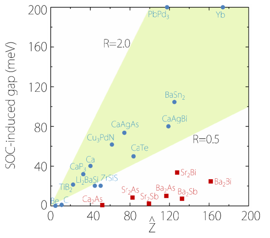
with denoting the effective SOC strength ( is generally relative to the atomic weight, due to the presence of Coulomb potential in the SOC Hamiltonian). One can find that nodal lines are gapped under SOC and the size of gap is relative to . Especially when the gap is sizable, the intrinsic properties of nodal lines are greatly destroyed. An investigation on typical NLSs preserving P and T symmetries indeed finds the size of gaps is positively related to expressed by the average atomic weight (), as shown in Fig. 1. More specifically, by defining the SOC-induced gap ratio [R, expressed as the SOC induced band gap divided by the ], it is found that typical NLSs proposed previously almost statistically distribute in a specific region with 0.5 R 2.0 (see Fig. 1). As a result, to obtain excellent NLSs with relatively small SOC-induced gaps, it is used to explore NLSs from materials without containing heavy elements, which however greatly restricts the scale of candidate materials for NLSs. Then, is it possible to develop excellent NLSs in heavy-element-containing materials? One way is to seek spin-orbit-stable nodal line under other protection mechanism (such as the reflection symmetry) rather than P and T symmetries. However, till now non-centrosymmetric PbTaSe2 is the only experimentally confirmed NLSs robust against SOC 50.
In this work, by combining the electronic properties of electrides, we propose that topological nodal line electrides (TNLEs) can serve as an effective way to realize ideal NLSs with negligible SOC-induced gaps, which can even be applied in heavy-elements containing systems. In electrides, the conduction electrons mostly originate from the so-called excess electrons, being localized in the interstitial sites of the lattice 51, 52. On the one hand, the unique electron states in the electrides are previously proposed to be favorable for obtaining band inversions needed for topological materials 53. As the results, several topological electrides such as Ca3Pb, Y2C, Sc2C, Sr2Bi, LaBr, HfBr, CsO3 are proposed 53, 54, 55. On the other hand, the excess electrons in electrides are not constrained by the nuclei electric field, thereby intrinsically manifest weak SOC effect. Therefore, TNLEs, where the nodal line band structure origins from the non-nucleus-constrained electrons, are expected to obtain ideal NLSs with nearly SOC-free nodal line states even containing heavy elements. Under this fresh viewpoint, in the following we demonstrate the feasibility of realizing TNLEs, and of developing ideal NLSs insensitive to SOC in PT symmetries preserving system.
2 2. COMPUTATIONAL METHODS
We carry out first-principles calculations by using the Vienna ab-initio simulation package based on the density functional theory (DFT) 56, 57. During our calculations, the exchange-correlation potential is chosen as generalized gradient approximation with the Perdew-Burke-Ernzerhof (PBE) realization 58. The nonlocal Heyd-Scuseria-Ernzerhof (HSE06) hybrid functional is also used to check the band structure 59. The cutoff energy during the calculations is chosen as 450 eV. To sample the Brillouin zone (BZ), a 11117 and 15159 -centered k-meshes are performed during the structural optimization and the self-consistent calculations. The force and energy convergence criteria are set as 0.001 eV/Å and 10-7 eV, respectively. The surface states are calculated using the slab model with thickness of 33 unit cells, realized by the OPENMX software package 60. The structural models are visualized via the VESTA software.
3 3. RESULTS AND DISCUSSIONS
After an exhaustive material screening, we find the family of A2B (A = Ca, Sr, Ba; B= As, Sb, Bi) materials are potential candidates for TNLEs. To be noted, one of the A2B materials, namely Sr2Bi has been proposed to possess both electride and nodal line characters without considering SOC quite recently 53. Unfortunately, the previous work did not make detailed discussions on the SOC effect of Sr2Bi. Thus, the A2B materials are still an excellent choice to study the properties of TNLEs.
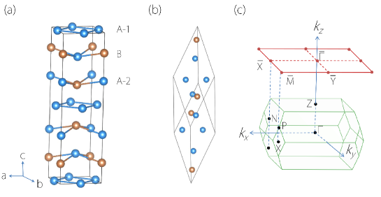
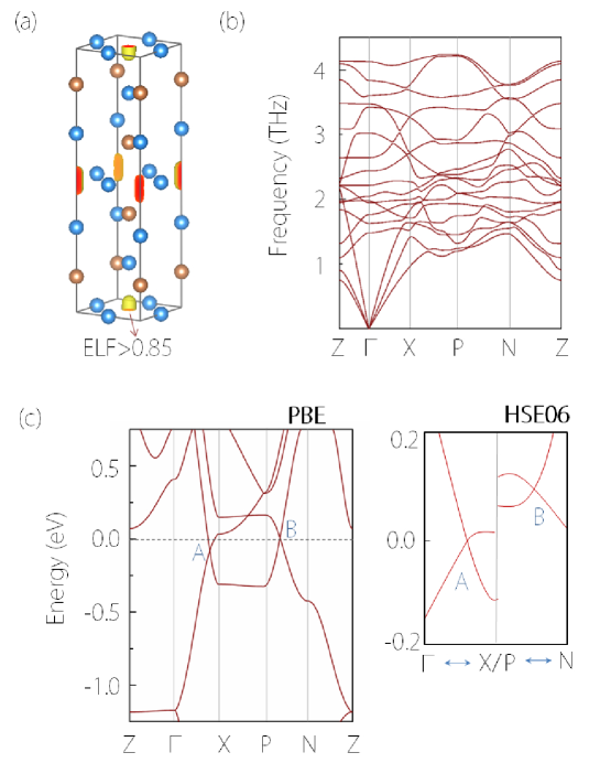
The A2B compounds possess a tetragonal lattice structure with the space group I4/mmm (No. 139). Fig. 2(a) shows the conventional cell of A2B compounds, where one group of A atoms (A-1) situate at the 4c Wyckoff sites (0, 0.5, 0), and the other group of A atoms (A-2) and B atoms are at the 4e Wyckoff sites (0, 0, /’), respectively. One conventional cell contains two units of primitive cell, and the primitive cell representation is shown in Fig. 2(b). Moreover, these A2B compounds are all existing materials that have already been synthesized experimentally 61, 62, 63, 64, 65, 66, 67. To further convince their stability, we calculate the phonon dispersions for the A2B materials [see Fig. 3(b) and Supplementary Information 68]. The phonon dispersions show that, these A2B materials (except Ba2As) have no imaginary mode throughout the BZ, indicating most of them are dynamically stable. Moreover, in A2B compounds, both P and T symmetries preserve.
Since most of A2B compounds have similar electronic structures, in the following we use Sr2Sb as a concentrate example. Considering the normal charge of atoms, Sr2Sb has the charge state of [Sr2Sb]+e-, which contains one excess electron for per formula. The electron localization function (ELF) index shows the degree of electron localization and is proved effective to identify electrides 69, 54, 53, 55, 70, 71: if the target material yields large ELF values (usually 0.75) in the interstitial lattice region, it can be considered as a potential electride. The three-dimensional (3D) ELF graph of Sr2Sb is shown in Fig. 3(a), where we adopt the ELF isosurface value as large as 0.85. We can clearly observe that ELF values lager than 0.85 all occur in the interstitial region, indicating Sr2Sb is a potential electride. The distribution of excess electrons in Sr2Sb is quite similar with that in Sr2Bi 53. Then we come to the band structure of Sr2Sb. Without considering SOC, as shown in Fig. 3(c), near the Fermi level there exist two band crossing points: point A at -0.079 eV along the X path, and point B at 0.007 eV along the PN path. Further calculations show Sr2Sb indeed undergoes band inversions near the Fermi level. To be specific, along the X path, the two inverted bands have the B1u and A1g representations of the D2h point group at the X point; and along the PN path, they have the B2 and A1 representations of the D2d point group at the P point. Both points A and B have double degeneracy without counting spin, and they are not isolate nodal points because both P and T symmetries preserve in Sr2Sb. Similar band structure has also been observed in Sr2Bi previously 53. It is well known that, the PBE functional usually underestimates the size of band gap in semimetals. So we check the band structure of Sr2Sb by using the hybrid HSE06 functional. From Fig. 3(c), we can clearly observe that the two crossing points A and B retain under HSE06 calculation.
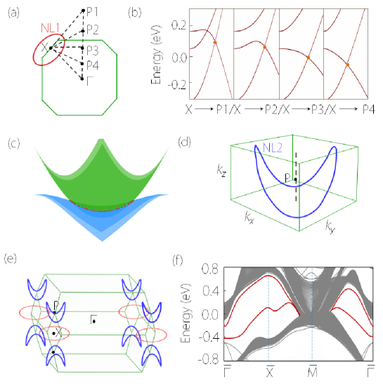
A careful scan of the band structure finds points A and B belong to two separated nodal lines. Point A belong to a nodal line centering the X point in the kx-ky plane, which enjoys additional protection of the mirror symmetry in the plane. As shown in Fig. 4(a) and 4(b), we can always obtain a linear band crossing point along the k-path starting from the X point in the plane. The shape and the band dispersion of the nodal line can be clearly shown by the 3D plotting of the band structure in the kz = 0 plane, as shown in Fig. 4(c). Here we denote the nodal line as nodal line 1 (NL1) [see Fig. 4(a)]. Point B belong to another nodal line (denoted as NL2) centering the P point. Different with NL1, NL2 does not reside on a specific plane but manifests a snakelike profile in the 3D Brillouin zone, as shown in Fig. 4(d). As the result, Sr2Sb possesses two kinds of nodal lines in the k-space [see Fig. 4(e)]. Nodal line semimetals usually characterize drumhead surface states. For Sr2Sb, we show the (001) surface band structure in Fig. 4(f). We can observe clear drumhead surface states originating from the nodal lines. With preserving both electride and nodal line signatures, Sr2Sb is a typical TNLE. Beside Sr2Sb, we find other six A2B materials including Ca2As, Sr2As, Sr2Bi, Ba2As, Ba2Sb, and Ba2Sb in A2B materials are also excellent TNLEs, while the rest Ca2Sb and Ca2Bi are only ordinary electrides without nodal line band structures 68.
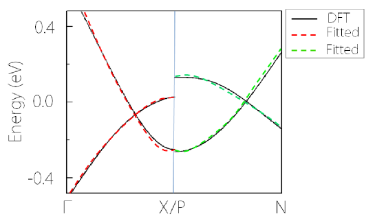
To further convince the DFT calculations, we construct effective models to describe the nodal lines. For NL1, the crossing bands have irreducible representations B1u and A1g at the X point. Using them as basis, we can obtain the effective Hamiltonian (up to k-quadratic order) as:
| (5) |
where . For NL2, the crossing bands possess irreducible representations B2 and A1 at the P point. And the effective Hamiltonian yields to be:
| (8) |
where . In above Hamiltonian, the parameters including , , , , E, F, and G are material-specific. The fitted band structure from the modal and the DFT results are shown in Fig. 5, which exhibit a good agreement.
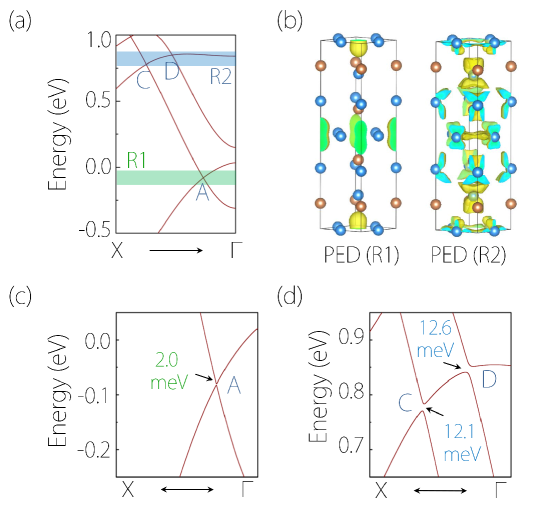
As mentioned above, the nodal lines in Sr2Sb are protected by the coexistence of P and T symmetries, and they will be gapped when SOC is taken into account. However, for electride Sr2Sb, the nodal lines are mostly contributed by the non-nucleus-constrained electrons, thus the SOC-induced gaps are expected to quite small although both Sr and Sb are heavy elements. This insight has been verified by our computations. In Fig. 6(a), we show the enlarged SOC-absence band structure of Sr2Sb along the X path, which includes crossing point A of NL1 (see the shadowed region R1). We calculate the partial electron density (PED) of R1 (-0.129 eV to -0.029 eV) to identify the electron distributions around crossing point A. As shown in the left panel of Fig. 6(b), we find the electrons for R1 origin from interstitial electrons. After including SOC, the band structure of crossing point A is indeed nearly unaffected, where the SOC-induced gap is negligible [2.0 meV, see Fig. 6(c)]. Beside crossing point A, we notice their exist other two band crossing points [points C and D in the shadowed region R2, see Fig. 6(a)]. Being Different with R1, the band structure in R2 is no longer contributed by interstitial electrons but by traditional bonding electrons, as shown by the PED graph for R2 [see the right panel of Fig. 6(b)]. As a result, the SOC-induced gaps at crossing points C and D are several times larger than that at point A [see Fig. 6(c) and 6(d)]. This indicates the size of SOC-induced gap is quite relate to the distribution of electrons. In TNLE Sr2Sb, the nodal lines are almost contributed by the interstitial electrons and are nearly unaffected when SOC is included.
Then we make a comparison between present TNLEs A2B compounds and existing typical NLSs. As shown in Fig. 1, the TNLEs in A2B materials have very small SOC-induced gaps and all situate far below the region of 0.5R2.0, indicating nodal lines in TNLEs have significantly smaller SOC-induced gaps comparing with traditional NLSs. Therefore, TNLEs are indeed excellent NLSs with pronounced nodal line character. It should be noted that, in TNLEs the SOC-induced gaps at different parts of the nodal line may be different because of the hybridization with orbitals of the interstitial bands. Beside the band structure at X path, we have also checked the SOC effect at other parts of the nodal line. Our calculations show that the SOC-induced gap does not change much at different k-paths in these A2B materials. To be specific, the SOC-induced gaps along the nodal line vary in 2.6 meV in Sr2Sb, 1.8 meV in Ca2As, 3.2 meV in Sr2As, 9.8 meV in Sr2Bi, 4.6 meV in Ba2As, 3.9 meV in Ba2Sb, 6.7 meV in Ba2Bi, respectively. Moreover, we also find the SOC-induced gaps can be tailored by tuning the distribution or localization of electrons around the nodal lines in TNLEs 68. The controllable SOC-induced gaps make TNLEs further practical to realize the nodal line states.
Before closing, we would like to emphasize that, the main focus of our work is quite different from previous works. In particular, in Ref.[ 53], Hirayama et al. proposed that electrides can also obtain band inversions which are needed for topological materials including topological insulating and topological semimetal phases. They also gave out several candidate materials (including Sr2Bi) for these topological phases in electrides. However, they neither made detailed study on the electronic structures of topological electrides under SOC, nor focused on topic of TNLEs for realizing small SOC-induced gaps in nodal lines.
4 4. SUMMARY
In summary, by promoting the realization of TNLEs in A2B (A = Ca, Sr, Ba; B= As, Sb, Bi) materials, we provide new insight on designing excellent NLSs with the nodal line structure nearly unaffected by the SOC effect. TNLEs possess both the electronic signatures of nodal lines and electrides. Especially, in TNLEs the nodal lines are mostly contributed by interstitial electrons, which are nearly unconstrained by the nuclei, thus SOC has weak impact on nodal lines even containing heavy elements. Besides, unlike traditional NLSs, we find the SOC-induced gaps in TNLEs are tunable by external perturbations such as lattice strain. TNLEs provide excellent platform to realize the exotic properties from the intrinsic nodal line state.
5 Conflicts of interest
There are no conflicts to declare.
6 Acknowledgements
The authors thank Shan Guan and Zhiming Yu for helpful discussions. This work is supported by National Natural Science Foundation of China (Grants No. 11904074), Natural Science Foundation of Hebei Province (Grants No. E2019202222 and No. E2016202383) and the National Key R&D Program of China (Grants No. 2016YFA0300600), the NSF of China (Grants No. 11734003), and the Project of Scientific Research for High Level Talent in Colleges and Universities of Hebei Province (No. GCC2014042). One of the authors (X.M. Zhang) acknowledges the financial support from Young Elite Scientists Sponsorship Program by Tianjin. One of the author (G.D. Liu) acknowledges the financial support from Hebei Province Program for Top Young Talents. One of the authors (B. Fu) acknowledge Sichuan Normal University for financial support (No. 341829001).
References
- 1 Wan, X.; Turner, A. M.; Vishwanath, A.; Savrasov, S. Y. Topological Semimetal and Fermi-Arc Surface States in the Electronic Structure of Pyrochlore Iridates. 2011, 83, 205101.
- 2 Murakami, S. Phase Transition between the Quantum Spin Hall and Insulator Phases in 3D: Emergence of a Topological Gapless Phase. 2007, 9, 356.
- 3 Burkov, A. A.; Balents, L. Weyl Semimetal in a Topological Insulator Multilayer. 2011, 107, 127205.
- 4 Weng, H.; Fang, C.; Fang, Z.; Bernevig, B. A.; Dai, X. Weyl Semimetal Phase in Noncentrosymmetric Transition-Metal Monophosphides. 2015, 5, 011029.
- 5 Huang, S. M.; Xu, S. Y.; Belopolski, I.; Lee, C. C.; Chang, G.; Wang, B. K.; Alidoust, N.; Bian, G.; Neupane, M.; Zhang, C.; Jia, S.; Bansil, A.; Lin, H.; Hasan, M. Z. A Weyl Fermion Semimetal with Surface Fermi Arcs in the Transition Metal Monopnictide TaAs Class. 2014, 6, 7373.
- 6 Young, S. M.; Zaheer, S.; Teo, J. C. Y.; Kane, C. L.; Mele, E. J.; Rappe, A. M. Dirac Semimetal in Three Dimensions. 2012, 108, 140405.
- 7 Wang, Z.; Sun, Y.; Chen, X.-Q.; Franchini, C.; Xu, G.; Weng, H.; Dai, X.; Fang, Z. Dirac Semimetal and Topological Phase Transitions in A3Bi (A=Na, K, Rb). 2012, 85, 195320.
- 8 Wang, Z.; Weng, H.; Wu, Q.; Dai, X.; Fang, Z. Three-dimensional Dirac Semimetal and Quantum Transport in Cd3As2. 2013, 88, 125427.
- 9 Yang, B.-J.; Nagaosa, N. Classification of Stable Three-Dimensional Dirac Semimetals with Nontrivial Topology. 2014, 5, 4898.
- 10 Borisenko, S.; Gibson, Q.; Evtushinsky, D.; Zabolotnyy, V.; Bchner, B.; Cava, R. J. Experimental Realization of a Three-Dimensional Dirac Semimetal. 2014, 113, 027603.
- 11 Weng, H.; Liang, Y.; Xu, Q.; Yu, R.; Fang, Z.; Dai, X.; Kawazoe, Y. Topological Node-Line Semimetal in Three-Dimensional Graphene Networks. 2015, 92, 045108.
- 12 Chen, Y.; Xie, Y.; Yang, S. A.; Pan, H.; Zhang, F.; Cohen, M. L.; Zhang, S. Nanostructured Carbon Allotropes with Weyl-like Loops and Points. 2015, 15, 6974.
- 13 Yang, S. A.; Pan, H.; Zhang, F. Dirac and Weyl Superconductors in Three Dimensions. 2014, 113, 046401.
- 14 Zhong, C.; Chen, Y.; Xie, Y.; Yang, S. A.; Cohen, M. L.; Zhang, S. B. Towards Three-Dimensional Weyl-Surface Semimetals in graphene networks. 2016, 8, 7232.
- 15 Liang, Q.-F.; Zhou, J.; Yu, R.; Wang, Z.; Weng, H. Node-Surface and Node-Line Fermions from Nonsymmorphic Lattice Symmetries. 2016, 93, 085427.
- 16 Wu, W.; Liu, Y.; Li, S.; Zhong, C.; Yu, Z.; Sheng, X.; Zhao, Y.; Yang, S. Nodal surface Semimetals: Theory and Material Realization. 2018, 97, 115125.
- 17 Zhang, X. M.; Yu, Z.-M.; Zhu, Z. M.; Wu, W. K.; Wang, S.-S.; Sheng, X.-L.; Yang, S. A. Nodal Loop and Nodal Surface States in the Ti3Al Family of Materials. 2018, 97, 235150.
- 18 Singha, R.; Pariari, A.; Satpati, B.; Mandal, P. Large Nonsaturating Magnetoresistance and Signature of Nondegenerate Dirac Nodes in ZrSiS. 2017, 114, 2468.
- 19 Ali, M. N.; Schoop, L. M.; Garg, C.; Lippmann, J. M.; Lara, E.; Lotsch, B.; Parkin, S. Butterfly Magnetoresistance, Quasi-2D Dirac Fermi Surface and Topological Phase Transition in ZrSiS. arXiv:1603.09318.
- 20 Wang, X.; Pan, X.; Gao, M.; Yu, J.; Jiang, J.; Zhang, J.; Zuo, H.; Zhang, M.; Wei, Z.; Niu, W.; Xia, Z.; Wan, X.; Chen, Y.; Song, F.; Xu, Y.; Wang, B.; Wang, G.; Zhang, R. Evidence of Both Surface and Bulk Dirac Bands and Anisotropic Nonsaturating Magnetoresistance in ZrSiS. 2016, 2, 1600228.
- 21 Guan, S.; Yu, Z.-M.; Liu, Y.; Liu, G.-B.; Dong, L.; Lu, Y.; Yao, Y.; Yang, S. A. Artificial Gravity Field, Astrophysical Analogues, and Topological Phase Transitions in Strained Topological Semimetals. 2017, 23, 2.
- 22 Liu, Y.; Yu, Z.-M.; Yang, S. A. Transverse Shift in Andreev Reflection. 2017 (R), 96, 121101.
- 23 Kim, Y.; Wieder, B. J.; Kane, C. L.; Rappe, A. M. Dirac Line Nodes in Inversion-Symmetric Crystals. 2015, 115, 036806.
- 24 Yu, R.; Weng, H.; Fang, Z.; Dai, X.; Hu, X. Topological Node-Line Semimetal and Dirac Semimetal State in Antiperovskite Cu3PdN. 2015, 115, 036807.
- 25 Yamakage, A.; Yamakawa, Y.; Tanaka, Y.; Okamoto, Y. Line-Node Dirac Semimetal and Topological Insulating Phase in Noncentrosymmetric Pnictides CaAgX (X = P, As). 2016, 85, 013708.
- 26 Huang, H.; Liu, J.; Vanderbilt, D.; Duan, W. Topological Nodal-Line Semimetals in Alkaline-Earth Stannides, Germanides, and Silicides. 2016, 93, 201114.
- 27 Schoop, L. M.; Ali, M. N.; Straber, C.; Topp, A.; Varykhalov, A.; Marchenko, D.; Duppel, V.; Parkin, S. S. P.; Lotsch, B. V.; Ast, C. R. Dirac Cone Protected by Non-Symmorphic Symmetry and Three-Dimensional Dirac Line Node in ZrSiS. 2016, 7, 11696.
- 28 Neupane, M.; Belopolski, I.; Hosen, M. M.; Sanchez, D. S.; Sankar, R.; Szlawska, M.; Xu, S.-Y.; Dimitri, K.; Dhakal, N.; Maldonado, P.; et al. Observation of Topological Nodal Fermion Semimetal Phase in ZrSiS. 2016, 93, 201104.
- 29 Hu, J.; Tang, Z.; Liu, J.; Liu, X.; Zhu, Y.; Graf, D.; Myhro, K.; Tran, S.; Lau, C. N.; Wei, J.; Mao, Z. Evidence of Topological Nodal-Line Fermions in ZrSiSe and ZrSiTe. 2016, 117, 016602.
- 30 Du, Y.; Tang, F.; Wang, D.; Sheng, L.; Kan, E.-J.; Duan, C.-G.; Savrasov, S. Y.; Wan, X. CaTe: a New Topological Node-Line and Dirac Semimetal. 2017, 2, 3.
- 31 Li, R. H.; Ma, H.; Cheng, X.; Wang, S.; Li, D.; Zhang, Z.; Li, Y.; Chen, X.-Q. Dirac Node Lines in Pure Alkali Earth Metals. 2016, 117, 096401.
- 32 Hirayama1, M.; Okugawa1, R.; Miyake, T.; Murakami S. Topological Dirac Nodal Lines and Surface Charges in fcc Alkaline Earth Metals. 2016, 8, 14022.
- 33 Zhang, X. M.; Jin, L.; Dai, F. X.; Liu, G. D. Highly Anisotropic Type-II Nodal Line State in Pure Titanium Metal. 2018, 112, 122403.
- 34 Zhang, X. M.; Jin, L.; Dai, F. X.; Liu, G. D. Topological Type-II Nodal Line Semimetal and Dirac Semimetal State in Stable Kagome Compound Mg3Bi2. 2017, 8, 4814.
- 35 Xu, Q.; Yu, R.; Fang, Z.; Dai, X.; Weng, H. Topological Nodal Line Semimetals in the CaP3 Family of Materials. 2017, 95, 045136.
- 36 Zhang, X. M.; Yu, Z.-M.; Sheng, X.-L.; Yang, H. Y.; Yang, S. A. Coexistence of Four-Band Nodal Rings and Triply Degenerate Nodal Points in Centrosymmetric Metal Diborides. 2017, 95, 235116.
- 37 Feng, X.; Yue, C.; Song, Z.; Wu, Q.; Wen, B. Topological Dirac Nodal-Net Fermions in AlB2-type TiB2 and ZrB2. 2018, 2, 014202.
- 38 Zhang, X. M.; Yu, Z.-M.; Lu, Y. H.; Sheng, X.-L.; Yang, H. Y.; Yang, S. A. Hybrid Nodal Loop Metal: Unconventional Magnetoresponse and Material Realization. 2018, 97, 125143.
- 39 Zhang, X. M.; Jin, L.; Dai, X. F.; Chen, G. F.; Liu, G. D. Ideal Inner Nodal Chain Semimetals in Li2XY (X = Ca, Ba; Y = Si, Ge) Materials. 2018, 9, 5358.
- 40 Sheng, X.-L.; Nikoli, B. K. Monolayer of the 5d Transition Metal Trichloride OsCl3: A Playground for Two-dimensional Magnetism, Room-Temperature Quantum Anomalous Hall Effect, and Topological Phase Transitions. 2018, 95, 201402.
- 41 Liu, G. D.; Jin, L.; Dai, X. F.; Chen, G. F.; Zhang, X. M. Topological Phase with a Critical-Type Nodal Line State in Intermetallic CaPd. 2018, 98, 075157.
- 42 Li, S.; Liu, Y.; Fu, B.; Yu, Z.-M.; Yang, S. A.; Yao, Y. Almost Ideal Nodal-Loop Semimetal in Monoclinic CuTeO3 Material. 2018, 97, 245148.
- 43 Zhu, Z.; Liu, Y.; Yu, Z.-M.; Wang, S.-S.; Zhao, Y. X.; Feng, Y.; Sheng, X.-L.; Yang, S. A. Quadratic Contact Point Semimetal: Theory and Material Realization. 2018, 98, 125104.
- 44 Zhang, T.-T.; Yu, Z.-M.; Guo, W.; Shi, D.; Zhang, G.; Yao, Y. From Type-II Triply Degenerate Nodal Points and Three-Band Nodal Rings to Type-II Dirac Points in Centrosymmetric Zirconium Oxide. 2017, 8, 5792.
- 45 Li, S.; Yu, Z.-M.; Liu, Y.; Guan, S.; Wang, S.-S.; Zhang, X.; Yao, Y.; Yang, S. A. Type-II Nodal Loops: Theory and Material Realization. 2017, 96, 081106.
- 46 Yu, Z.-M.; Wu, W.; Sheng, X.-L.; Zhao, Y. X.; Yang, S. A. Quadratic and Cubic Nodal Lines Stabilized by Crystalline Symmetry. 2019, 99, 12116.
- 47 Ahn, K.-H.; Pickett, W. E.; Lee, K.-W. Coexistence of Triple Nodal Points, Nodal Links, and Unusual Flat Bands in Intermetallic APd3 (A = Pb, Sn). 2018, 98, 035130.
- 48 Wang, X.-B.; Ma, X. M.; Emmanouilidou, E.; Shen, B.; Hsu, C. H.; Zhou, C. S.; Zuo, Y.; Song, R. R.; Xu, S. Y.; Wang, G.; et al. Topological Surface Electronic States in Candidate Nodal-Line Semimetal CaAgAs. 2017, 96, 161112.
- 49 Fang, C.; Weng, H. M.; Dai, X.; Fang, Z. Topological Nodal Line Semimetals. 2016, 25, 115201.
- 50 Bian, G.; Chang, T.; Sankar, R.; Xu, S.; Zheng, H.; Neupert, T.; Chiu, C.; Huang, S.; Chang, G.; Belopolski, I. Topological Nodal-Line Fermions in Spin-Orbit Metal PbTaSe2. 2016, 7, 10556.
- 51 Dye, J. L.; DeBacker, M. G. Physical and Chemical Properties of Alkalides and Electrides. 1987, 38, 271.
- 52 Walsh, A.; Scanlon, D. O. PbO2: from Semi-metal to Transparent Conducting Oxide by Defect Chemistry Control 2013, 1, 3525.
- 53 Hirayama, M.; Matsuishi, S.; Hosono, H.; Murakami, S. Electrides As a New Platform of Topological Materials. 2018, 8, 031067.
- 54 Zhang, X. M.; Guo, R. K.; Jin, L.; Dai, X. F.; Liu, G. D. Intermetallic Ca3Pb: a Topological Zero-dimensional Electride Material. 2018, 6, 575.
- 55 Park, C.; Kim, S. W.; Yoon, M. First-Principles Prediction of New Electrides with Nontrivial Band Topology Based on One-Dimensional Building Blocks. 2018, 120, 026401.
- 56 Kresse, G.; Joubert, D. From Ultrasoft Pseudopotentials to the Projector Augmented-Wave Method. Phys. Rev. B: Condens. Matter Mater. Phys. 1999, 59, 1758-1775.
- 57 Kresse, G.; Hafner, J. Ab Initio Molecular Dynamics for Liquid Metals. Phys. Rev. B: Condens. Matter Mater. Phys. 1993, 47, 558-561.
- 58 Perdew, J. P.; Burke, K.; Ernzerhof, M. Generalized Gradient Approximation Made Simple. Phys. Rev. Lett. 1996, 77, 3865-3868.
- 59 Heyd, J.; Scuseria, G. E.; Ernzerhof, M. Hybrid Functionals Based on a Screened Coulomb Potential. J. Chem. Phys. 2003, 118, 8207.
- 60 See http://www.openmx-square.org.
- 61 Pearson, W. B.; Kristallogr, Z.; Pearson, W. B. The Cu2Sb and Related Structures. Zeitschrift für Kristallographie - Crystalline Materials. 1985, 171, 23.
- 62 Martinez-Ripoll, M.; Haase, A.; Brauer, G. The Crystal Structure of Sr2Sb. 1973, 29, 1715.
- 63 Eisenmann, B.; Schaefer, H. The Crystal Structures of Ca2Sb and Ca2Bi. Zeitschrift für Naturforschung B 1974, 29, 13-15.
- 64 Better, B.; Huetz, A.; Nagorsen, G. Die Strukturen der Intermetallischen Verbindungen Sr2As, Ba2As, Sr5As3 und Ba5As3. Zeitschrift fuer Metallkunde 1976, 67, 118-119.
- 65 Martinez-Ripoll, M.;Haase, A.;Brauer, G. The Crystal Structure of Sr2Sb, Zeitschrift fuer Kristallographie 1985, 171, 23-39.
- 66 Eisenmann, B.; Deller, K. Zur Kenntnis der Erdalkaliantimonide und -wismutide Sr2 Bi, Ba2 Sb, Sr5Bi3, Ba5Sb3 und Ba5Bi3, Zeitschrift fuer Kristallographie 1985, 171, 23-29.
- 67 Martinez-Ripoll, M.; Haase, A.; Brauer, G. The Crystal Structure of BaBi, Acta Crystallographica B 1974, 30, 2003-2004.
- 68 See supplementary information for phonon band structures, ELF graphs and band structures of A2B materials, and strain effect in Ba2Bi.
- 69 Zhang, Y.; Wang, H.; Wang, Y.; Zhang, L.; Ma, Y. Computer-Assisted Inverse Design of Inorganic Electrides. 2017, 7, 011017.
- 70 Huang, H.; Jin, K.-H.; Zhang, S.; F. Liu. Topological Electride Y2C. 2018, 18, 1972.
- 71 Zhu, S.-C.; Wang, L.; Qu, J.-Y.; Wang, J.-J.; Frolov, T.; Chen, X.-Q.; Zhu, Q. Skin Lesion Segmentation Using U-Net and Good Training Strategies. 2018, .11314.