Quantum Motion Technologies, Nexus, Discovery Way, Leeds, LS2 3AA, United Kingdom \alsoaffiliationQuantum Motion Technologies, Nexus, Discovery Way, Leeds, LS2 3AA, United Kingdom \alsoaffiliationQuantum Motion Technologies, Nexus, Discovery Way, Leeds, LS2 3AA, United Kingdom \alsoaffiliationDept. of Electronic & Electrical Engineering, UCL, London WC1E 7JE, United Kingdom
Remote capacitive sensing in two-dimensional quantum-dot arrays
Abstract
We investigate gate-induced quantum dots in silicon on insulator nanowire field-effect transistors fabricated using a foundry-compatible fully-depleted silicon-on-insulator (FD-SOI) process. A series of split gates wrapped over the silicon nanowire naturally produces a bilinear array of quantum dots along a single nanowire. We begin by studying the capacitive coupling of quantum dots within such a 22 array, and then show how such couplings can be extended across two parallel silicon nanowires coupled together by shared, electrically isolated, ‘floating’ electrodes. With one quantum dot operating as a single-electron-box sensor, the floating gate serves to enhance the charge sensitivity range, enabling it to detect charge state transitions in a separate silicon nanowire. By comparing measurements from multiple devices we illustrate the impact of the floating gate by quantifying both the charge sensitivity decay as a function of dot-sensor separation and configuration within the dual-nanowire structure. Keywords: Quantum dots, Reflectometry, floating gate coupler, electrostatic coupling
Spin qubits in silicon demonstrate the fundamental properties required for scaled quantum computation, with state-of-the-art one- and two-qubit operations demonstrating control fidelities approaching the requirements for fault-tolerant quantum error correction 1, 2, 3, 4. While all control elements have been integrated into single devices with scalable readout mechanisms 5, much effort is now being focused into developing these devices from simple laboratory prototype structures into scaled arrays of qubits capable of eventually yielding a quantum advantage 6, 7. The promise of a highly developed materials system and mature fabrication industry, together with the success of laboratory, and industry-grade prototype silicon-metal-oxide-semiconductor (SiMOS) quantum-dot based devices 8 has led to the proposition of several approaches to foundry-compatible scaling into grid-based architectures of quantum dot arrays. These approaches range from densely-packed qubits with next-nearest-neighbour couplings 9, dot arrays partially-populated with qubits 10 and arrays with qubit sites linked via mediating structures for remote qubit-qubit coupling 11.
SiMOS devices which form quantum dots in the corners of silicon nanowires naturally produce bilinear dot arrays 12, which allow for proximal sensor integration for both charge 13, 14, 15, 16 and spin states 17 through dispersive measurements using gate-based reflectometry. The advantages of these integrated sensors can be extended by mechanisms for off-wire coupling, to sense the state of dots located in remote locations within the quantum dot array. In order to enhance the capacitive coupling between spatially separated quantum dots, studies in planar GaAs/AlGaAs and Ge/Si heterostructures and carbon nanotubes have exploited a floating gate 18, 19, 20; a metallic electrode which is galvanically isolated from, but capacitively coupled to, its immediate environment.
Here, utilising a single quantum dot sensor, we demonstrate a system capable of performing both proximal and remote capacitive charge sensing within a array of quantum dots distributed across two parallel nanowires. We compare these results with geometrically identical single-wire variants, serving as an isolated array. Each 2 array is formed on a single silicon nanowire (SiNW), and all devices described here are located in the same die, fabricated from a fully-depleted silicon-on-insulator (FD-SOI) process 21. Our approach uses floating gate electrodes to capacitively couple a sensor dot to quantum dots on remote nanowires, whilst maintaining sensitivity to adjacent dots within the local nanowire. We quantify the sensitivity to charge movement within these two schemes by experimentally benchmarking the device capacitance matrix, supported by cryo-SiMOS simulations.
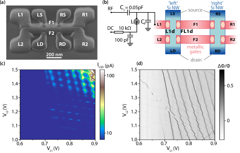
The scanning electron micrograph (SEM) image in Fig. 1(a) shows a device of the type used in these remote sensing experiments. Two parallel nanowires, with centre-to-centre spacing of 200 nm, are fabricated with two central floating gates F1 and F2 wrapping the interior edges of both, spanning the gap between the two silicon structures. Gates F1 and F2 are capacitively coupled to the surrounding gates by proximity, but are otherwise electrically isolated. All gate structures are separated by a SiN spacer which increases cross capacitance. The device is further encapsulated by 300 nm of silicon oxide, above which an additional top gate T is deposited utilising a back-end metallisation layer (not shown). Full geometric details for the family of devices compared in this work can be found in Supplementary §I. The charge sensor for these experiments consists of a two-terminal structure in which a charge island is connected to single reservoir, known as a single electron box (SEB) 13, 14, 15, 16, 17. The sensor is configured under a single gate, L1, utilising the dot L1d, which is coupled to an electron reservoir and measured using the reflectometry circuit depicted in Fig. 1(b). With this configuration, the addition of electrons to the dots within the left nanowire can be inferred from either the transport current through the device with source-drain bias mV, seen in Fig. 1(c), or the S11 reflectometry signal (measured at V) seen in Fig. 1(d), which maps the same gate voltage space. Both measurements contain structure attributed to multiple dots within the 22 array of the left nanowire. Due to the low transport current through the device, discerning the occupancy of the dots via transport is a significant challenge, while the capacitive shifts due to the addition of an electron are readily detected in reflectometry, which can probe all proximal quantum dots down to the last electron transition (Supplementary §I). The SEB dot-lead transitions at lower SEB electron numbers are less visible due to the reduction in tunneling rates below the RF frequency of the reflectometry measurement 22.
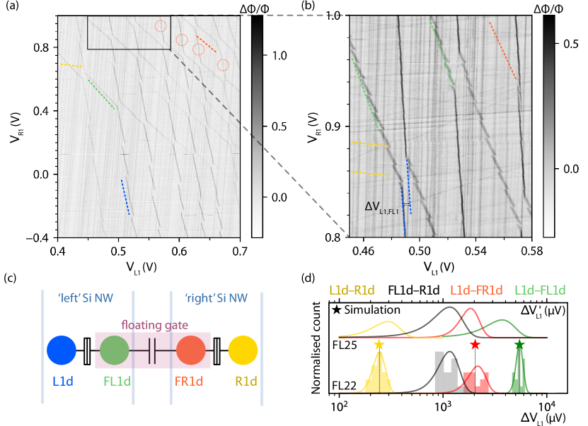
As the floating gates are galvanically isolated, we use the top metal gate T to assist in the accumulation of quantum dots under floating gates, primarily via the mutual capacitance between gates F1, F2 and T (see Supplementary §V). Simultaneously, both and are set to a depletion mode to avoid formation of quantum dots under gates L2, R2 and F2, to effectively ‘shut-off’ the lower half of the device by electron depletion. With the voltage sweep of and shown in Fig. 2(a), and noting the influence of the floating gate F1 which is capacitively coupled to both active gates, we can load electrons into dots L1d and R1d, as well as dots FL1d and FR1d, from their neighbouring reservoirs. Charge detection of these four distinct quantum dots is shown in the stability diagram measured in the reflectometry phase signal Fig. 2(a), and includes the remote sensing of dots FR1d and R1d, located in the ‘right’ SiNW, detected by the sensor dot L1d, located in the ‘left’ SiNW. The sensor dot L1d is estimated to hold 10 electrons in this voltage range, where dot-reservoir charge transitions can be observed directly as a phase peak. We can then identify the remaining three different quantum dots capacitively coupled to the sensor through two complementary approaches:
-
(1)
Through the ratio of cross capacitance between the two active gate voltages and and the dot.
-
(2)
Through direct charge detection by the sensor dot, assessing the magnitude of the capacitive shift upon the sensor.
For the voltage map between and shown in Fig. 2(a), each of the four dots capacitively couple to the L1 and R1 electrodes with differing strength, and we illustrate the four quantum dots present with reference to the colour code shown in the capacitance connectivity diagram of Fig. 2(c). In Figs. 2(a) and 2(b), the blue dashed line indicates dot-lead charge transition of the SEB, L1, which naturally has the highest lever arm to . The other three coloured dashed lines highlight each remaining variety of dot-lead charge transition. The floating-gate-induced quantum dot in the left SiNW FL1d (green) is more strongly coupled to the sensor gate L1 due to its proximity, while in the SiNW on the right, the other floating-gate-induced quantum dot FR1d (red) and gate-induced quantum dot R1d (yellow) are more strongly coupled to gate R1. When quantum dot FL1d is sufficiently occupied, the increase in tunnel rates allows for FL1d dot-lead transitions to also be directly detected in the reflectometry phase shift signal. This signal allows us to trace back the number of electrons in sensor dot L1d (see Supplementary §I). This approach can be further quantified by comparing the cross-capacitance ratios calculated as the degree to which gate L1 influences the other dot-lead transitions in voltage space. Assuming , this method yields , , . A significant drop in the cross-capacitance ratio is therefore apparent for groups of dots under spatially separated gates.
A second quantitative approach to distinguish the different quantum dots coupled to the sensor is to analyse the strength of the capacitive coupling between the sensor dot L1d and each of the remaining dots. In Fig. 2(d) we plot a histogram of the shifts , expressed in terms of the gate L1 voltage , arising from the capacitive shift in the sensor dot L1d due to the addition of an electron to some other dot 23. We use a peak-finding algorithm near a capacitive shift of interest in Fig. 2(b) and take the difference between the shifted dot-lead reflectometry peaks, extrapolated to the same value of . The capacitive shifts extracted in this way group naturally into three distinct sets, each corresponding to the transitions in another quantum dot indicated following the colour code in Fig. 2c). Being located in the same nanowire, FL1d (green) is the most strongly coupled to the sensor dot, while the other floating-gate-induced quantum dot FR1d (red), located in the remote nanowire, shows a slightly weaker coupling. The R1 gate-induced quantum dot R1d (yellow) in the remote nanowire shows the weakest coupling, but can still be detected. A normalized fit of the probability density function of each group provides the mean capacitive shift referenced against the sensor dot gate voltage: = 5.47 mV, = 2.16mV, = 0.243 mV. These values show good agreement to simulations of the capacitance matrix for this device structure (see Supplementary §III).
As certain charge transitions FL1d are directly visible in the phase response, we can also extract a corresponding capacitive shift between dots FL1d and R1d, which is the symmetric analogue to the sensor dot coupling through the floating gate to FR2d. Data corresponding to such shifts are shown in grey in Fig. 2d), and indeed fall within a similar range to . This asymmetry is not captured in our simulations and is most likely due to finite lithographic misalignment between the patterns of the nanowire and the split between the gates. Based on automated overlay controls and tools specifications we estimate that the cuts, although centered on the nanowires by design, are probably shifted by 5-10nm on a typical device. In our case, this asymmetry translates into stronger lever-arm parameters for the dots defined along the right edges of the nanowires, and is systematically observed in other devices 17, 24. Finally, to show the consistency of these values across different devices of the fabricated on the same die, we performed the same set of measurements on a second device and plot the extracted Gaussian fits to for each pair of dots on the same axis in Fig. 2(d).
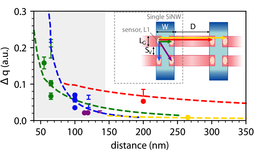
To demonstrate the enhancement of capacitive coupling arising from the floating gates, we compare results from floating gate devices with those from devices with similar dimensions containing only single, isolated silicon nanowires (see Supplementary §I). In order to facilitate the comparison of results from different devices, sensor dots and lever arms, we adopt a measure of the SEB sensitivity to the charge transitions in nearby quantum dots based on normalizing the voltage-referenced capacitive coupling by the addition voltage required to add an electron to the SEB: , where is the detected voltage shift in arising from coupling to dot , is the change in required to add an electron to the sensor dot L1d.
We first study the normalized SEB charge sensitivity within a 22 quantum dot array located in a single silicon nanowire. Here we can compare the capacitive coupling between dots formed on opposite edges of the nanowire, between adjacent dots formed along a common SiNW edge, and also between diagonally coupled, next-nearest neighbour quantum dots. These configurations are shown in the inset of Fig. 3, which also illustrates configurations for sensing dots in a neighbouring SiNW, with coupling facilitated through the floating gate. The data in Fig. 3 compare three single-nanowire devices, each consisting a 22 quantum dot array, as well as the corresponding single-nanowire arrays within two floating-gate devices. The intra-wire normalised sensitivities fall off quickly with increasing separation between the quantum dots, though a single power law cannot be used to describe the overall trend with distance for all couplings, due to the difference in mutual capacitance for dots located on the same or opposite edges of the nanowire.
Modelling the quantum dot as conducting ellipsoids we calculate the Maxwell capacitance matrix for varying center-to-center dot separation , along with other nanowire design parameters (full details of the simulation method and relation to device dimensions are given in Supplementary §I–V). Each of the parametric sweeps from the simulations (dashed lines in Fig. 3) settles to a power law attributed to each sensor-dot configuration: nearest-neighbour couplings along the edge of the nanowire (L1d-L2d) or across the nanowire (L1d-FL1d) have couplings which decay approximately as or respectively, over the range of distances studied here. Data for a next-nearest neighbour configuration L1d-FL2d, where the dots are positioned diagonally across the wire, is shown for completeness but is not modelled. For the ‘remote sensing’ configuration where charge transitions are detected through the floating gate, the normalized capacitive coupling is sustained over a much greater distance, as reflected in the experimental data and simulations. By sweeping the floating gate length (approximated to be the SiNW separation, ) simulations show that the two dots under each corner of the floating gate have a coupling which is dominated by the second-order capacitive coupling via the floating gate at these distances, and decays only as (see Supplementary §VI). Combined with the additional spacing of the nanowire width local to the SEB, this results in an coupling decay for the dot L1d-FR1d configuration which can be approximated as in the range studied here. As a result, the mutual capacitive shift for dot L1d-FR1d remains relatively high, even at distances exceeding 300 nm, as shown in Fig. 3.
Coupling the sensor to dot R1d now involves three degrees of separation from the sensor, with a corresponding drop in sensitivity for short separations. However, the action of the floating gate leads to a much more gradual decay in sensitivity with distance that goes as in our simulations. As a result, for distances above nm, the floating gate mediated coupling between dots arranged on opposite edges of different nanowires exceeds that from two dots on opposite edges of the same silicon nanowire (see Supplementary §VI). Furthermore, the charge distribution due to floating gate geometry could be optimised to yield a stronger absolute coupling, while maintaining the much more gradual decay with distance 25.
Our experimental measurements and simulations indicate decays in capacitive coupling strength which fall off more slowly than , as previously observed within arrays of Si/SiGe planar quantum dots 26, 27. However, such measurements were made within planar quantum dot devices with a high density of metallic gate electrodes, expected to screen mutual capacitive coupling. Indeed, considering only the first-order approximations to capacitive couplings, our simulations also show decays that approach (see Supplementary §VI). In contrast, the devices studied here contained a relatively low density of metallic gate electrodes, and the fabrication of the split-gates involved etching of metal that was replaced by SiN. The result is a reduced decay rate in sensitivity as a function of dot-dot separation — most strikingly when facilitated by the capacitively coupled floating gate. Instead of screening charge movement, the floating gate propagates the effect of charge movement over a distance to be chosen as a design parameter, coupling charge between two otherwise separate silicon structures. While the simulations are able to capture well the trends in the different classes of coupling, the residual spread in experimental values across the measurements may be due to the asymmetry in realistic devices, not captured by the simulations, which can influence not only the dot to dot geometrical distance but also the device lever arms.
The capacitive shifts we measured between QDs, both locally and on distinct nanowires, are well above the full-width at half-maximum (FWHM) of the SEB dot-lead charge transition (see Supplementary §II). Assuming a Lorentzian lineshape for the measured SEB charge transition, any capacitive shift greater than twice the FWHM gives at least of the maximum sensor contrast (e.g. for spin-dependent tunneling readout). Based on our simulations and the intrinsic FWHM of the sensor transition of 0.24 mV, dot L1d-FR1d type couplings mediated by the floating gate could be used to achieve spin readout for distances up to 500 nm without a reduction in readout contrast.
In addition to applications for sensing, capacitive coupling has been used to realise local multi-qubit interactions in a variety of systems, including singlet-triplet qubits 28 and charge qubits 29, 30. Meanwhile, several approaches to scaling quantum dot arrays pursue long-range coupling between qubits to facilitate the integration and fan-out of control electronics and suppress charge leakage 6, 11— solutions to realising such two-qubit gates include exploiting a RKKY mediating exchange interaction 31, 11 or coupling via a superconducting resonator 32. Multi-qubit operations utilising capacitive coupling via floating gates, coupling two singly-occupied planar dot structures, have been proposed to produce a spin-spin coupling Hamiltonian when the Zeeman energy and where are the Pauli matrices in the relevant qubit basis 25, which can be used to implement the iSWAP operation 33. Combining the assumptions within Ref [25] with the parameters of the devices studied here and spin-orbit coupling strength for silicon 34, we estimate a coupling of Hz under realistic device operating conditions between FL1d and FR1d with nanowire separation nm, which is too weak for practical applications. However, utilising the floating gate to couple two singlet-triplet qubits via 28, where is the identity matrix, exploits the much stronger electric-dipole coupling to achieve the CZ operation. For the nanowire geometry presented here (i.e. with singlet-triplet qubits arranged on each nanowire and the nearest dots of each pair separated by nm) we estimate Hz via the model in Ref. [25], made more favourable in this geometry due to reduced oxide thickness. In SiGe devices, coupling between charge qubits mediated by the mutual capacitance term 29, 30 has been demonstrated with a strength of 15 GHz over dot separations of 130 nm 30, while for the device geometry studied here our results predict Hz for dots separated by 200 nm on different nanowires.
We have demonstrated through experiments and simulation the effect of integrating floating gate electrodes to extend the sensitivity range of a single capacitive sensor, highlighting in particular the potential to couple quantum dots located on distinct silicon nanowires. Our measurements made the use of a single electron box charge sensor, while we note that a parallel study on similar devices illustrates an alternative mode for charge detection in such structures, with one nanowire acting as a single electron transistor that remotely senses the charge occupancy of dots on the other nanowire 35. In future devices with overlapping gate architecture 3, a second layer of gate electrodes could be used independently tune the quantum dots confined under the floating gates and achieve remote interactions. Given the substantial promise of spin qubits formed along quasi-1D arrays, along the edges of silicon nanowires 17, the enhanced capacitive couplings we measure using floating gates provide a potential route to couple qubits distributed across separate nanowires and thus for scaling in a second dimension.
The authors gratefully acknowledge the financial support from the European Union’s Horizon 2020 research and innovation programme under grant agreement No 688539 (http://mos-quito.eu); as well as the Engineering and Physical Sciences Research Council (EPSRC) through the Centre for Doctoral Training in Delivering Quantum Technologies (EP/L015242/1), QUES2T (EP/N015118/1) and the Hub in Quantum Computing and Simulation (EP/T001062/1).
References
- Yoneda et al. 2018 Yoneda, J.; Takeda, K.; Otsuka, T.; Nakajima, T.; Delbecq, M. R.; Allison, G.; Honda, T.; Kodera, T.; Oda, S.; Hoshi, Y.; Usami, N.; Itoh, K. M.; Tarucha, S. A quantum-dot spin qubit with coherence limited by charge noise and fidelity higher than 99.9%. Nat. Nanotechnol. 2018, 13, 102–106
- Xue et al. 2019 Xue, X.; Watson, T. F.; Helsen, J.; Ward, D. R.; Savage, D. E.; Lagally, M. G.; Coppersmith, S. N.; Eriksson, M. A.; Wehner, S.; Vandersypen, L. M. K. Benchmarking Gate Fidelities in a Si/SiGe Two-Qubit Device. Phys. Rev. X 2019, 9, 021011
- Zajac et al. 2018 Zajac, D. M.; Sigillito, A. J.; Russ, M.; Borjans, F.; Taylor, J. M.; Burkard, G.; Petta, J. R. Resonantly driven CNOT gate for electron spins. Science 2018, 359, 439–442
- Huang et al. 2019 Huang, W.; Yang, C. H.; Chan, K. W.; Tanttu, T.; Hensen, B.; Leon, R. C. C.; Fogarty, M. A.; Hwang, J. C. C.; Hudson, F. E.; Itoh, K. M.; Morello, A.; Laucht, A.; Dzurak, A. S. Fidelity benchmarks for two-qubit gates in silicon. Nature 2019, 569, 532–536
- Fogarty et al. 2018 Fogarty, M. A.; Chan, K. W.; Hensen, B.; Huang, W.; Tanttu, T.; Yang, C. H.; Laucht, A.; Veldhorst, M.; Hudson, F. E.; Itoh, K. M.; Culcer, D.; Ladd, T. D.; Morello, A.; Dzurak, A. S. Integrated silicon qubit platform with single-spin addressability, exchange control and single-shot singlet-triplet readout. Nat. Commun. 2018, 9, 4370
- Vandersypen et al. 2017 Vandersypen, L. M. K.; Bluhm, H.; Clarke, J. S.; Dzurak, A. S.; Ishihara, R.; Morello, A.; Reilly, D. J.; Schreiber, L. R.; Veldhorst, M. Interfacing spin qubits in quantum dots and donors—hot, dense, and coherent. npj Quantum Inf. 2017, 3, 34
- Jones et al. 2018 Jones, C.; Fogarty, M. A.; Morello, A.; Gyure, M. F.; Dzurak, A. S.; Ladd, T. D. Logical qubit in a linear array of semiconductor quantum dots. Physical Review X 2018, 8, 021058
- Maurand et al. 2016 Maurand, R.; Jehl, X.; Kotekar-Patil, D.; Corna, A.; Bohuslavskyi, H.; Laviéville, R.; Hutin, L.; Barraud, S.; Vinet, M.; Sanquer, M.; De Franceschi, S. A CMOS silicon spin qubit. Nat. Commun. 2016, 7, 13575
- Veldhorst et al. 2017 Veldhorst, M.; Eenink, H. G.; Yang, C. H.; Dzurak, A. S. Silicon CMOS architecture for a spin-based quantum computer. Nat. Commun. 2017, 8, 1766
- Li et al. 2018 Li, R.; Petit, L.; Franke, D. P.; Dehollain, J. P.; Helsen, J.; Steudtner, M.; Thomas, N. K.; Yoscovits, Z. R.; Singh, K. J.; Wehner, S.; Vandersypen, L. M. K.; Clarke, J. S.; Veldhorst, M. A crossbar network for silicon quantum dot qubits. Sci. Adv. 2018, 4, eaar3960
- Cai et al. 2019 Cai, Z.; Fogarty, M. A.; Schaal, S.; Patomäki, S.; Benjamin, S. C.; Morton, J. J. L. A Silicon Surface Code Architecture Resilient Against Leakage Errors. Quantum 2019, 3, 212
- Voisin et al. 2014 Voisin, B.; Nguyen, V.-H.; Renard, J.; Jehl, X.; Barraud, S.; Triozon, F.; Vinet, M.; Duchemin, I.; Niquet, Y.-M.; de Franceschi, S.; Sanquer, M. Few-Electron Edge-State Quantum Dots in a Silicon Nanowire Field-Effect Transistor. Nano Lett. 2014, 14, 2094–2098
- Urdampilleta et al. 2019 Urdampilleta, M. et al. Gate-based high fidelity spin readout in a CMOS device. Nat. Nanotechnol. 2019, 14, 737–741
- House et al. 2016 House, M. G.; Bartlett, I.; Pakkiam, P.; Koch, M.; Peretz, E.; Van Der Heijden, J.; Kobayashi, T.; Rogge, S.; Simmons, M. Y. High-Sensitivity Charge Detection with a Single-Lead Quantum Dot for Scalable Quantum Computation. Phys. Rev. Appl. 2016, 6, 044016
- Chanrion et al. 2020 Chanrion, E. et al. Charge detection in an array of CMOS quantum dots. 2020, arXiv:2004.01009. arXiv.org e-Print archive. \urlhttp://arxiv.org/abs/2004.01009 (accessed September 4,2020)
- Ansaloni et al. 2020 Ansaloni, F.; Chatterjee, A.; Bohuslavskyi, H.; Bertrand, B.; Hutin, L.; Vinet, M.; Kuemmeth, F. Single-electron control in a foundry-fabricated two-dimensional qubit array. 2020, arXiv:2004.00894. arXiv.org e-Print archive. \urlhttp://arxiv.org/abs/2004.00894 (accessed September 4,2020)
- Ciriano-Tejel et al. 2020 Ciriano-Tejel, V. N.; Fogarty, M. A.; Schaal, S.; Hutin, L.; Bertrand, B.; Gonzalez-Zalba, M. F.; Li, J.; Niquet, Y. M.; Vinet, M.; Morton, J. J. L. Spin readout of a CMOS quantum dot by gate reflectometry and spin-dependent tunnelling. 2020, arXiv:2005.07764. arXiv.org e-Print archive. \urlhttp://arxiv.org/abs/2005.07764 (accessed September 4,2020)
- Chan et al. 2002 Chan, I. H.; Westervelt, R. M.; Maranowski, K. D.; Gossard, A. C. Strongly capacitively coupled quantum dots. Appl. Phys. Lett. 2002, 80, 1818–1820
- Churchill et al. 2009 Churchill, H. O. H.; Bestwick, A. J.; Harlow, J. W.; Kuemmeth, F.; Marcos, D.; Stwertka, C. H.; Watson, S. K.; Marcus, C. M. Electron–nuclear interaction in 13C nanotube double quantum dots. Nat. Phys. 2009, 5, 321–326
- Hu et al. 2007 Hu, Y.; Churchill, H. O. H.; Reilly, D. J.; Xiang, J.; Lieber, C. M.; Marcus, C. M. A Ge/Si heterostructure nanowire-based double quantum dot with integrated charge sensor. Nat. Nanotechnol. 2007, 2, 622–625
- Hutin et al. 2016 Hutin, L.; Maurand, R.; Kotekar-Patil, D.; Corna, A.; Bohuslavskyi, H.; Jehl, X.; Barraud, S.; De Franceschi, S.; Sanquer, M.; Vinet, M. Si CMOS platform for quantum information processing. 2016 IEEE Symp. VLSI Technol. 2016; pp 1–2
- Gonzalez-Zalba et al. 2015 Gonzalez-Zalba, M. F.; Barraud, S.; Ferguson, A. J.; Betz, A. C. Probing the limits of gate-based charge sensing. Nat. Commun. 2015, 6, 6084
- van der Wiel et al. 2002 van der Wiel, W. G.; De Franceschi, S.; Elzerman, J. M.; Fujisawa, T.; Tarucha, S.; Kouwenhoven, L. P. Electron transport through double quantum dots. Rev. Mod. Phys. 2002, 75, 1–22
- Ibberson et al. 2020 Ibberson, D. J.; Lundberg, T.; Haigh, J. A.; Hutin, L.; Bertrand, B.; Barraud, S.; Lee, C.-M.; Stelmashenko, N. A.; Robinson, J. W. A.; Vinet, M.; Gonzalez-Zalba, M. F.; Ibberson, L. A. Large dispersive interaction between a CMOS double quantum dot and microwave photons. 2020, arXiv:2004.00334. arXiv.org e-Print archive. \urlhttp://arxiv.org/abs/2004.00334 (accessed September 4,2020)
- Trifunovic et al. 2012 Trifunovic, L.; Dial, O.; Trif, M.; Wootton, J. R.; Abebe, R.; Yacoby, A.; Loss, D. Long-Distance Spin-Spin Coupling via Floating Gates. Phys. Rev. X 2012, 2, 011006
- Zajac et al. 2016 Zajac, D. M.; Hazard, T. M.; Mi, X.; Nielsen, E.; Petta, J. R. Scalable Gate Architecture for a One-Dimensional Array of Semiconductor Spin Qubits. Phys. Rev. Appl. 2016, 6, 054013
- Neyens et al. 2019 Neyens, S. F.; MacQuarrie, E.; Dodson, J.; Corrigan, J.; Holman, N.; Thorgrimsson, B.; Palma, M.; McJunkin, T.; Edge, L.; Friesen, M.; Coppersmith, S.; Eriksson, M. Measurements of Capacitive Coupling Within a Quadruple-Quantum-Dot Array. Phys. Rev. Appl. 2019, 12, 064049
- Shulman et al. 2012 Shulman, M. D.; Dial, O. E.; Harvey, S. P.; Bluhm, H.; Umansky, V.; Yacoby, A. Demonstration of Entanglement of Electrostatically Coupled Singlet-Triplet Qubits. Science 2012, 336, 202–205
- Li et al. 2015 Li, H. O.; Cao, G.; Yu, G. D.; Xiao, M.; Guo, G. C.; Jiang, H. W.; Guo, G. P. Conditional rotation of two strongly coupled semiconductor charge qubits. Nat. Commun. 2015, 6, 7681
- MacQuarrie et al. 2020 MacQuarrie, E. R.; Neyens, S. F.; Dodson, J. P.; Corrigan, J.; Thorgrimsson, B.; Holman, N.; Palma, M.; Edge, L. F.; Friesen, M.; Coppersmith, S. N.; Eriksson, M. A. Progress Towards a Capacitively Mediated CNOT Between Two Charge Qubits in Si/SiGe. 2020, arXiv:2003.06768. arXiv.org e-Print archive. \urlhttp://arxiv.org/abs/2003.06768 (accessed September 4,2020)
- Malinowski et al. 2019 Malinowski, F. K.; Martins, F.; Smith, T. B.; Bartlett, S. D.; Doherty, A. C.; Nissen, P. D.; Fallahi, S.; Gardner, G. C.; Manfra, M. J.; Marcus, C. M.; Kuemmeth, F. Fast spin exchange across a multielectron mediator. Nat. Commun. 2019, 10, 1196
- Borjans et al. 2020 Borjans, F.; Croot, X. G.; Mi, X.; Gullans, M. J.; Petta, J. R. Resonant microwave-mediated interactions between distant electron spins. Nature 2020, 577, 195–198
- Schuch and Siewert 2003 Schuch, N.; Siewert, J. Natural two-qubit gate for quantum computation using the XY interaction. Phys. Rev. A 2003, 67, 032301
- Tanttu et al. 2019 Tanttu, T.; Hensen, B.; Chan, K. W.; Yang, C. H.; Huang, W. W.; Fogarty, M.; Hudson, F.; Itoh, K.; Culcer, D.; Laucht, A., et al. Controlling spin-orbit interactions in silicon quantum dots using magnetic field direction. Physical Review X 2019, 9, 021028
- Gilbert et al. 2020 Gilbert, W.; Saraiva, A.; Lim, W. H.; Yang, C. H.; Laucht, A.; Bertrand, B.; Rambal, N.; Hutin, L.; Escott, C. C.; Vinet, M.; Dzurak, A. S. Single-electron operation of a silicon-CMOS 2x2 quantum dot array with integrated charge sensing. 2020, arXiv:2004.11558. arXiv.org e-Print archive. \urlhttp://arxiv.org/abs/2004.11558 (accessed September 4,2020)