Distinguishing the gapped and Weyl semimetal scenario in ZrTe5:
insights from an effective two-band model
Abstract
Here we study the static and dynamic transport properties of a low energy two-band model proposed previously in E. Martino et al. [PRL 122, 217402 (2019)], with an anisotropic in-plane linear momentum dependence, and a parabolic out-of-plane dispersion. The model is extended to include a negative band gap, which leads to the emergence of a Weyl semimetal (WSM) state, as opposed to the gapped semimetal (GSM) state when the band gap is positive. We calculate and compare the zero and finite frequency transport properties of the GSM and WSM cases. The properties that are calculated for the GSM and WSM cases are Drude spectral weight, mobility and resistivity. We determine their dependence on the Fermi energy and crystal direction. The in- and out-of-plane optical conductivities are calculated in the limit of the vanishing interband relaxation rate for both semimetals. The main common features are an in-plane and out-of-plane frequency dependence of the optical conductivity. We seek particular features related to the charge transport that could unambiguously point to one ground state over the other, based on the comparison with the experiment. Differences between the WSM and GSM are in principle possible only at extremely low carrier concentrations, and at low temperatures.
I Introduction
Zirconium pentatelluride, ZrTe5, is a layered material Okada et al. (1980); Jones et al. (1982); Whangbo et al. (1982); Shahi et al. (2018) which recently became a topic of intense research. This was mainly due to the experimental evidence Wang et al. (2018); Zhang et al. (2017); Yuan et al. (2016) of a 3D Dirac-like band structure in the vicinity of the point of the Brillouin zone, a novelty compared with the previously held belief of parabolic like valence bands Whangbo et al. (1982). One of the major signatures of a 3D Dirac-like band structure is the linearity in the optical conductivity with respect to photon energy above the Pauli threshold Ashby and Carbotte (2014). However, for recent optical and magneto-optical measurements Martino et al. (2019) suggest that the energy bands are not entirely linear, but posses an out-of-plane parabolic term as well.
Like in many other topological semimetals, in ZrTe5 the intrinsic energy scales are small. This makes it challenging to experimentally distinguish between different possible ground states Moreschini et al. (2016). The ambiguity of the bandgap — whether it is zero, finite and positive, or finite and negative — also opens a possibility that ZrTe5 may be a Weyl semimetal Liang et al. (2018), and not Dirac semimetal as previously stated Chen et al. (2015a, b). To distinguish between these two options, it is of interest to see how much their calculated charge transport quantities differ. This begs the question of whether one could interpret the same experimental data in different ways.
Based on the experiment and the ab initio calculation, we had previously introduced a simple low energy two-band model for ZrTe5, which was identified as gapped semimetal. The main features of the proposed effective Hamiltonian are the gapped and electron-hole symmetric eigenvalues. This is accompanied by the anisotropic linearity of the bands along the intralayer directions and the parabolic dispersion in the weakly dispersive out-of-plane direction. This model provided an explanation of experimental data Martino et al. (2019); Santos-Cottin et al. (2020), in particular the square-root dependence of the optical conductivity at very low photon energies, in contrast to the linear dependence found in 3D Dirac semimetals Ashby and Carbotte (2014); Tabert et al. (2016); Tabert and Carbotte (2016). It also allowed us to estimate the energy interval in which the simple two-band model applies.
In this work, we identify under which circumstances it is possible to distinguish between the gapped and Weyl semimetal scenario, specifically for ZrTe5. To do this, we generalize the Hamiltonian model to allow for a negative bandgap Mukherjee et al. (2019); Lu et al. (2015); Okugawa and Murakami (2014). By this simple change of the sign of the bandgap, we generate a minimal model Hamiltonian for Weyl semimetal. And so, by changing the sign of this parameter, we pass from a gapped semimetal (GSM) to the Weyl semimetal (WSM). The main difference lies in the shape of the bands at low energies. Contrary to the GSM case, the WSM case has a 3D linear-like bands in the close vicinity of the two Weyl points.
In the case, corresponding to transport, we calculate the total and the effective concentration of electrons. Since the effective concentration is direction dependent, it will explain the resistivity anisotropy as well as the carrier mobility.
All the three spatial components of the real part of the interband conductivity are evaluated for GSM and WSM cases, in the limit of vanishing relaxation rate. We find that, for both the GSM and WSM, at high photon energies the plane conductivity has a dependence, and in the direction it has a dependence when the external field energies are well above the bandgap value. For photon energies below the bandgap, the GSM optical conductivity is zero, while the WSM shows a dependence, similar to the 3D Dirac case.
Finite temperatures, with comparable to the Fermi energy, significantly alter the shape of the optical conductivity. This results in a linear-like optical conductivity, which can easily be mistaken for a signature of a gapless 3D Dirac dispersion. Finite interband relaxation values only slightly modify the general appearance of the real part of the conductivity, except in the bandgap region where the conductivity acquires a finite contribution proportional to the relaxation itself.
II Ab initio calculations and the model Hamiltonian
We have performed the ab initio band structure calculations of the orthorhombic phase of ZrTe5 using density functional theory (DFT) with the generalized gradient approximation Singh (1994, 1991); wie . Once the unit cell is finalized with the parameters Å, Å, and Å, a spin-orbit coupling is added to the electronic structure calculations. The results are shown in Fig. 1 with the valence band in blue, and the conduction band in red.
At small energies the material appears to be a semimetal with a small bandgap and the quasi-linear features in the vicinity of the point in the Brillouin zone. The effective model considered in Martino et al. (2019) is based on these basic features of the calculated band structure.
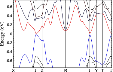
However, the problem lies in the values of the ab initio calculated parameters in Table 1, which deviate from the experimentally determined parameters Martino et al. (2019). In particular, the bandgap here is off by a factor of three, and in some references a factor of ten or more Xiong et al. (2017); Miller et al. (2018); Fan et al. (2017).
| exp | |||||
|---|---|---|---|---|---|
| DFT |
II.1 Effective two-band model
The Hamiltonian matrix implements the electron-hole symmetry of the valence bands, a positive energy band gap originating from the spin-orbit coupling, with the assumption of a free-electron like behavior in the (or axis) direction and linear energy dependence in the () plane. Here we expand the model to account for the Weyl phase by adding a negative bandgap. The Hamiltonian is thus
| (2.1) |
where the label differentiates between the GSM for the value , and the WSM for the value . Further, are Pauli matrices, are the velocities in the and directions, and we introduce with being the effective mass.
The diagonalization of Eq. (2.1) gives electron-hole symmetric eigenvalues
| (2.2) |
with the indices for the conduction () and valence () bands. Although trivial, the change from significantly alters the energies and single-particle properties. While the GSM phase is always gapped in this model, the WSM phase has two Weyl points in the Brillouin zone where the energy vanishes, . Expanding the WSM eigenvalues around these two points gives linear momentum eigenvalues,
| (2.3) |
where we can formally identify
| (2.4) |
In a third, trivial phase, a zero gap phase occurs when the bandgap is set to zero, .
For , we have a gapped phase in which the gap is -dependent, but it never changes its sign. Therefore, there is no interesting topology involved Tchoumakov et al. (2017). In contrast, for , we obtain a minimal model for a WSM. This model is spin degenerate simply because the Hamiltonian matrix is and not . Spin degeneracy is ensured by the centrosymmetric lattice of ZrTe5. Still, because we gain in simplicity, it is fitting to call this phase in a Hamiltonian model a Weyl semimetal phase Mukherjee et al. (2019); McCormick et al. (2017); Shen (2017).
II.2 Density of states
Here we calculate the density of states (DOS) for the energy dispersion from Eq. (2.2) for the GSM and WSM cases. By definition, the DOS per unit volume is,
| (2.5) |
Given the shape of the dispersions in Eq. (2.2), the sum is changed into an integral in a cylindrical coordinate system, by introducing the variables and ,
| (2.6) |
First, the delta function in Eq. (II.2) is decomposed with respect to the variable into a sum,
| (2.7) |
Here, are the four roots of the argument within the function: . Due to the absolute value, the outer set of points only brings a factor of in Eq. (II.2). The under the square root is relevant for further evaluation, as it will determine the upper limit of the integration for . Inserting Eq. (2.7) in Eq. (II.2), and by noticing that , we have
The upper limit of the integration is determined by the condition that the expression under the square root in Eq. (II.2) be positive. The first obvious constraint is , and the second depends on the sign and on the type .
We solve the WSM case () first. For , the subroot expression is well defined if . For , we have two additional constraints. If then , or else if , then . The integral in Eq. (II.2) for the WSM case with the constraints on can be most simply written by introducing the variable . Then
where is the Heaviside step function. If we introduce an auxiliary function ,
| (2.10) |
and the unit as
| (2.11) |
we can write the final result for DOS,
| (2.12) |
The GSM case () follows similarly. Inspecting the subroot function in Eq. (II.2), we see that makes the subroot expression negative and so we discard it. On the other hand, restricts to . From the upper limit we conclude that . Using the same substitution as in the WSM case, we have
| (2.13) |
which can be evaluated explicitly,
| (2.14) |
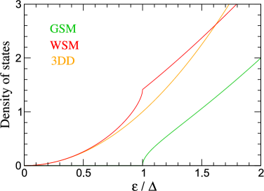
It is interesting to notice that the low energy limit, , of reduces to the 3D Dirac (3DD) case,
| (2.15) |
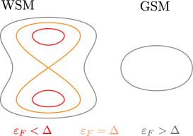
The three densities of states, Eqs. (II.2), (2.14) and (2.15) are shown in Fig. 2. The DOS in Eq. (2.15) is twice the value of a single Dirac cone since in the low-energy Weyl picture, there are two equal contributions of the Weyl points to the total DOS. This can be seen from Fig. 3, where the Fermi surface is shown for the WSM and GSM scenarios. When Fermi energy is below , Lifshitz transition takes place and the WSM Fermi surface contains two electron pockets which begin to merge at the Fermi energy . This energy corresponds to the van Hove discontinuity in the DOS, seen as a kink in Fig. 2.
III Zero-temperature dc quantities
Having evaluated the DOS, we can proceed to calculate the often used transport quantities: the total concentration of conduction electrons ; the effective concentration of conducting electrons ; the resistivity ; and the electron mobility . All calculations in this Section are performed for for both the GSM and WSM cases.
III.1 Total electron concentration
The total carrier concentration is defined in the usual way,
| (3.1) |
where the summation over bands is implicitly assumed. At the Fermi-Dirac function is , and it simply modifies the upper integration limit. In integrating Eq. (3.1) with the DOS as defined in the previous section, we define a second auxiliary function ,
| (3.2) |
In this way, we are able to write the total concentration of electrons in the GSM case as
| (3.3) |
and similarly for the WSM case,
| (3.4) |
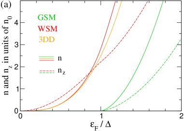
The total concentration is plotted in Fig. 4(a) (full lines), for the GSM and WSM cases as a function of , in units of .
III.2 Effective electron concentration
The effective concentration of the conduction electrons is a direction dependent variable defined as Ashcroft and Mermin (1976); Dressel and Grüner (2002)
| (3.5) |
Here, is a Cartesian component, is the electron bare mass and is the electron group velocity. At , , which excludes all states except those at the Fermi level. The expression in Eq. (3.5) forms a part of the Drude formula,
| (3.6) |
where defines the Drude spectral weight related to the plasmon frequency, which is most easily seen in a reflectivity measurement. A common feature of the dispersions in Eq. (2.2) is the similar shape of their electron velocity in the direction, . We have inserted this velocity in Eq. (3.5), so we can evaluate for GSM and WSM case using the approach outlined in Sec. II.2. The result for the GSM is
| (3.7) |
and similarly for the WSM,
| (3.8) |
Both concentrations, Eqs. (3.7) and (3.8), have the same high energy limit, when . For energies below , only remains finite,
| (3.9) |
and gives the same result as found for the 3D Dirac dispersion Ashby and Carbotte (2014); Tabert et al. (2016) once we substitute Eq. (2.4) in Eq. (3.8). The case is obtained by a simple exchange in Eqs. (3.7) and (3.8).
A different behavior is anticipated for the , primarily because of the different velocity dependence . Solving for calls for the definition of yet another auxiliary function,
| (3.10) |
which then yields
| (3.11) |
and
| (3.12) |
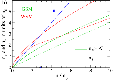
From Table 1 we see that , allowing us to plot both concentrations, Eqs. (3.11) and (III.2), in Fig. 4(a) in units of as a function of the ratio . What we see from Fig. 4(a) is that both the total and the effective electron concentrations are very similar in shape for the GSM and WSM at Fermi energies above , where the . This trend is reversed for low Fermi energies, , where only the WSM concentrations remain finite. In addition, the effective electron concentration for the Weyl case, Eq. (III.2), has a weak hump at . This is produced by a kink in the DOS. The effective concentrations for the gapped, Eq. (3.7), and the Weyl case, Eq. (3.8), in comparison to the total carrier concentrations, Eqs. (3.3) and (III.1), are times larger if we take the values from the Table 1. The parameter is used in plotting the concentrations in Fig. 4(b). To that end, we introduce a unit of concentration for the cases:
| (3.13) |
This unit has a value of if the experimental values from Table 1 are used. Experimentally, it is natural to express the transport quantities as functions of the doping or the total carrier concentration . This procedure is carried out numerically by expressing as a function of the total concentration, Eq. (3.3) for the WSM and Eq. (III.1) for the GSM, and then inserting this into the effective concentrations, Eqs. (3.7) through (III.2).
Figure 4(b) shows the effective GSM and WSM carrier concentrations, , as a function of the total carrier concentration . The WSM case (red lines) is visibly different form the GSM case (green lines). Through this difference we might obtain insight on how to distinguish the GSM case from the WSM case, at zero temperature, based on the resistivity anisotropy. This is done in the following Section.
The zero gap case follows trivialy from Eq. (3.3) which, after setting , gives the total concentration
| (3.14) |
Setting may also be applied to all other effective concentrations.
III.3 Mobility and resistivity

The conduction electron mobility is defined through the following relation Mahan (1993),
| (3.15) |
Through comparison with Eq. (3.6) we conclude
| (3.16) |
Based on the results for WSM and GSM cases for in-plane effective concentrations, , we have,
| (3.17) |
The large ratio is key in the above expression, meaning that a very large intralayer carrier mobility in ZrTe5, reaching up to cm(Vs), is related to a high Fermi velocity, (Table 1).
For the direction, the limit of gives the identical mobility for the WSM and GSM cases:
| (3.18) |
For the GSM, when the Fermi level hits just above . This is a usual result for a parabolic like dispersion with an effective mass , but interestingly it comes with a different numerical prefactor than the high energy limit of carrier mobility [Eq. (3.18)]. The WSM case is
| (3.19) |
which is equivalent to Eq. (3.17) once we use the substitution in Eq. (2.4).
The direction-dependent resistivity anisotropy is best seen trough the resistivity ratio , where defined from the Drude formula [Eq. (3.6)] for the GSM and WSM cases,
| (3.20) |
The in-plane resistivity ratio is straightforward and equal for the GSM and WSM cases. Using Eqs. (3.7) and (3.8), and Table 1, we get
| (3.21) |
This constant value is shown in Fig. 5 in blue.
In contrast to Eq. (3.21), the out-of-plane anisotropy strongly depends on the total concentration of electrons . This is seen in Fig. 5 where is plotted for the WSM and GSM cases as a function of . The upper limit of the plot is . For meV (Table 1), this corresponds to a Fermi energy of meV [Eq. (3.3)] in the GSM and meV [Eq. (III.1)] in the WSM case. In the low concentration limit, and are visibly different. While decreases monotonically from the maximal value of ; increases to a maximum located at , only to start decreasing for larger doping. This qualitatively different behavior of as a function of is the key to distinguish the GMS from the WSM in transport, under the condition that the samples can be chemically or electrostatically doped. Using expressions for effective carrier concentrations, Eqs. (3.6), (3.7) and (3.8), gives in the high concentration limit ,
| (3.22) |
This is shown in Fig. 5, where the splitting between the GSM and WSM follows from Eq. (3.22). In the opposite, low-energy limit when , the resistivity anisotropy is only meaningful in the WSM case where it is given by,
| (3.23) |
The resistivity anisotropies containing and directions follow analogously.
In the zero-gap case, is the same as Eq. (3.21), while is
| (3.24) |
an exact result over the entire range of concentration . Contrary to the GSM and WSM cases, both of which have finite values in the limit as seen in Fig. 5, the zero gap resistivity anisotropy, Eq. (3.24), diverges for small concentrations. This makes it a valuable indicator about the possible nature of the ground state.
IV Optical conductivity
When dealing with the optical response of an insulator or a semimetal, we normally use a conductivity formula containing a phenomenological interband relaxation rate . This interband is different from the intraband or Drude relaxation rate . In the two-band model, the interband conductivity is Kupčić et al. (2013)
| (4.1) |
In Eq. (4.1) we have introduced and the -dependent interband current vertices Kupčić et al. (2016) which are calculated in Appendix A for the WSM and GSM cases. Here we limit our discussion to the interband conductivity, knowing that a Drude term will always be present for a finite carrier density.
We analytically evaluate the real part of the conductivity tensor [Eq. (4.1)] in the limit . Considering only , the above expression (4.1) becomes
| (4.2) |
The Fermi-Dirac distributions in the above expression are simplified by taking into account the symmetry of the bands and the fact that the expression Eq. (4.2) is finite only for . We can then write the distribution function as
| (4.3) |
In the case, the above expression simplifies to , which describes the suppression of the interband transitions due to the Pauli blocking.
Calculation of follows analogously to the procedure outlined in previous sections. First we insert the interband current vertex, Eq. (A), into Eq. (4.2). The new variables are , and . After the transformation into the cylindrical system, we have
| (4.4) |
The solution to Eq. (IV) will be facilitated by introducing yet another auxiliary function,
| (4.5) |
Here we mention briefly some of the properties of . For just above , Eq. (4.5) reduces to . In the opposite limit (), we have . In all cases of interest, function can be well enough approximated by
| (4.6) |
To simplify our optical expressions, we define the units of conductivity, . They depend on the component ,
| (4.7) |
In continuation, we determine the optical conductivities separately for the GSM and WSM cases.
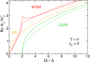
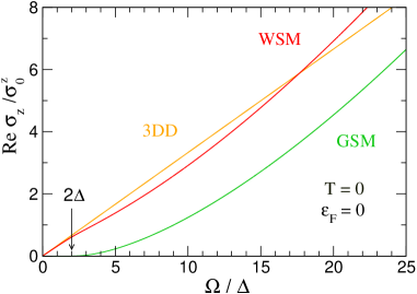
IV.1 Optical conductivity for gapped semimetal case
The real part of the -component of the interband conductivity is given for the GSM () case by
| (4.8) |
Figure 6 shows the optical conductivity determined from Eq. (4.8) for the intrinsic case where , in other words . If an approximate expression shown in Eq. (4.6) is used in Eq. (4.8), it leads to a simplified version of the interband conductivity,
| (4.9) |
This approximate result is also shown in Fig. 6 with a dashed line, and it is rather close to the exact expression in Eq. (4.8).
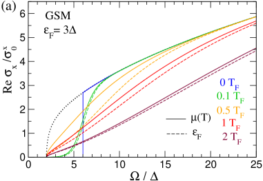
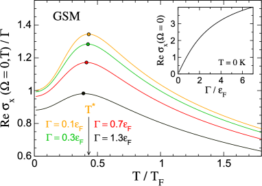
Figure 7 shows the real part of the optical conductivity determined from Eq. (4.8) for various temperatures given in units of Fermi temperature, . We consider two cases. In the first case, we neglect the temperature variation of the electron chemical potential by fixing . In the second case, we include the temperature dependence of the chemical potential , and we calculate self-consistently from the relation Eq. (3.1) inserted into Eq. (4.3). The difference between using or diminishes at , and at high temperatures, . The reason for this is that at low temperatures , and at high temperatures the Fermi-Dirac distribution is smeared beyond the temperature dependence of . Interestingly, in the intermediate temperature range where , the optical conductivity develops a linear-like energy dependence. This quasi-linear optical response of shown in Fig. 7 can easily be mistaken for a sign of a 3D Dirac-like band structure.
The derivation of is essentially the same, the only difference arising from the current vertex which changes the ratio of the electronic velocities. The resulting real part of the optical conductivity is,
| (4.10) |
The differences are, just like in the transport, addressed in Sec. III, in the direction. This is a result of a different current vertex [Eq. (1.10)]. Introducing the fifth and final auxiliary function ,
| (4.11) |
we can write the component of the optical conductivity in a more compact way,
| (4.12) |
Energy properties of Eq. (4.12) are determined by the function , whose limit determines the high energy components of the real part of the conductivity
| (4.13) |
This function is plotted in Fig. 9 and it is visibly different from the plane conductivity [Fig. 7(a)], which behaves as . However, unfortunately the -axis optical conductivity is experimentally much less accessible.
IV.2 Optical conductivity for Weyl semimetal case
Similar analysis applies to the WSM case. Once again using the shorthand introduced in Eq. (4.5), the real component of the optical conductivity along axis is,
| (4.14) |
The basic features of this function are displayed in Fig. 6, where Eq. (IV.2) is plotted for the case that and taking the full expression Eq. (4.5), shown in full line, versus the approximation Eq. (4.6), shown in a dashed line. The linearity of is clearly seen for . By expanding (IV.2) for small energies , we have indeed,
| (4.15) |
in accordance with the 3D Dirac spectrum Ashby and Carbotte (2014). At the energy , a direct transition between two hyperbolic points in the energies of Eq. (2.2) occurs, and manifests itself as a kink in the curve, just as it did in the DOS. In the case of , the optical conductivity becomes
| (4.16) |
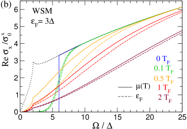
Figure 7(b) shows the WSM optical conductivity from Eq. (IV.2) plotted for various temperatures . As in the previous calculation, the case of constant and the have been addressed. The was calculated self-consistently from Eq. (3.1). In addition to the similar temperature dependent features like in the GSM case, we see a persistent kink at at all temperatures. This kink comes from the merging of the Weyl cones and the related direct transitions between van Hove points.
IV.3 Optical conductivity for zero gap case
In the zero gap phase, the GSM and WSM expressions from the previous two Sections reduce to the same result. Since , for the components of the conductivity we get
| (4.18) |
The above conductivity is shown in Fig. 6. In a similar way, the component of the real part of the optical conductivity is obtained by setting in Eq. (4.12), which makes Eq. (4.13) an exact result.
IV.4 Optical conductivity anisotropy
The ratio of the [Eq. (4.8)] and [Eq. (4.10)] components of the real part of the optical conductivity is very much analogous to the analysis followed in Sec. III.3. For both the GSM and WSM, the optical conductivity anisotropy is identical,
| (4.19) |
and given by an expression analogous to the resistivity anisotropy in Eq. (3.20). For the majority of anisotropic Dirac systems, the velocity ratio is Morinari et al. (2009); Rusponi et al. (2010); Ryu et al. (2018), and ZrTe5 is no exception with its . In some systems, this ratio was reported to be an order of magnitude larger Park et al. (2011). Another equally important parameter responsible for the amplitude of the optical conductivity is the effective mass , hidden in [Eq. (2.4)], which should be very large, for the model described in Eq. (2.1) to be applicable. The effective mass plays a role in the following ratio which involves the component conductivity,
| (4.20) |
Similarly to the case [Eq. (3.22)], because of the very large characteristic energy eV, the above ratio is extremely small in the energy range where the model [Eq. (2.1)] is valid.
It is worth mentioning that are nicely described by the approximative function, Eq. (4.6), compared to the exact one in Eq. (4.5), as it can be seen from Fig. 6. If we go back to the Sec. II.2, we may notice that with Eq. (4.6) is in fact proportional to . This is in accordance with the usual rule-of-thumb derivation of the optical conductivity Dressel and Grüner (2002), where the current vertex is assumed to be a constant in Eq. (1.11). While this simplification works well for the case, it utterly fails for the direction [see Eq. (1.10)].
IV.5 Finite interband relaxation rate and finite temperature effects in the GSM case
Finite interband relaxation contribution to the is calculated numerically from the expression Eq. (4.2). Finite modifies the onset of the single particle excitation in comparison with the analytical result in Eq. (IV), which then gives a nonzero value of the static interband conductivity in the band gap region, even at zero temperatures.
The increase of the static interband conductivity can be clearly seen in the insert of Fig. 9, where is shown as a function of . Deriving this functional dependence is straightforward in the case of a 3D Dirac dispersion Tabert et al. (2016). In the GSM case, we can find the result numerically,
| (4.21) |
The above expression shows a linear increase of the interband conductivity for the interband damping , and a stronger deviation for higher values of .
The temperature dependence of is plotted in Fig. 9 for various values of the interband relaxation . The strong increase of the static value of the conductivity is noteworthy. This has already been addressed and is shown in the inset of Fig. 9. At finite temperatures, there is a maximum located at , which can be traced back to the smearing of the Fermi-Dirac function with increasing . The maximum slowly shifts towards lower values as we increase .
This calculation is relevant in the intrinsic case, when . In the absence of a Drude component, the interband contribution will then dominate the response. We emphasize that the Drude component is not considered anywhere in Section IV, although it is present, and may be large at finite temperatures or finite carrier densities.
V Conclusions
In this article we have addressed the static and dynamic transport properties of the Weyl and gapped semimetal described by an effective two-band model of the valence electrons. The model implements a linear dispersion in the in-plane directions and a parabolic dispersion in the out-of-plane direction, coupled to a positive band gap in the gapped case, or a negative band gap in the Weyl case. The transport properties in the static limit, such as the direction dependent resistivity and mobility, are predominately influenced by large values of intralayer electron velocities. The transport properties are similar in the Weyl and gapped cases at high values of Fermi energy. For energies lower than the band gap, only the Weyl phase has a finite contribution, and this limit corresponds to the well-known 3D Dirac dispersion case.
In the limit of low concentrations, we show how to distinguish between Weyl phase, finite gap, or zero gap phase, using resistivity anisotropy in the out-of-plane direction.
The interband conductivity shows a dependence on photon energy in the in plane and a dependence in the out-of-plane direction for both gapped and Weyl semimetal cases. The model predicts that the in-plane conductivity anisotropy is equal to the squared Fermi velocity ratio, just like it is the case for the transport. The model also shows out-of-plane conductivity anisotropy, although proportional to , is insignificantly larger due to the comparatively large velocity . The effects of a finite interband relaxation constant give a finite contribution to the interband conductivity as well as a maximum in temperature at , associated with the smearing of the Fermi-Dirac distribution at high temperatures and small Fermi energies.
Finally, we showed that it is not possible to distinguish Weyl and gapped semimetal at higher temperatures and/or higher carrier concentrations, within our effective model. At high temperatures, both of these cases strongly resemble 3D Dirac semimetal. This means that the measurement of optical conductivity alone should not be used to classify the topological nature of the ground state, if at zero temperature. Similar conclusion is valid for dc transport. If the doping is high, there is way to distinguish between Weyl and gapped semimetal.
At very low doping, transport gives different ratios of the interlayer and intralayer resistivities for the gapped and Weyl cases. In the case of ZrTe5, it remains an experimental challenge how to reach such low carrier concentrations.
Note: While finalizing our work, we became aware of the recent work of Wang and Li Wang and Li (2020), whose results are in agreement with our findings for interband conductivity of our model.
VI Acknowledgments
Z.R. acknowledges helpful discussions with M.O. Goerbig. A. A. acknowledges funding from the Swiss National Science Foundation through project PP00P2_170544. Z. R. was funded by the Postdoctoral Fellowship of the Swiss Confederation. This work has been supported by the ANR DIRAC3D. We acknowledge the support of LNCMI-CNRS, a member of the European Magnetic Field Laboratory (EMFL). Work at Brookhaven National Laboratory was supported by the U. S. Department of Energy, Office of Basic Energy Sciences, Division of Materials Sciences and Engineering under Contract No. DE-SC0012704.
Appendix A current verticies
In the general form of the Hamiltonian
| (1.1) |
the interband current vertices can be shown to be Kupčić et al. (2016),
| (1.2) |
where are the elements of unitary matrix defined as
| (1.3) |
with the definitions,
| (1.4) |
Therefore in the general case of Eq. (1.1), Eq. (1.2) gives
| (1.5) |
Now we can determine the above derivations for the Hamiltonian in Eq. (2.1). We obtain
| (1.6) |
and
| (1.7) |
and trivially
| (1.8) |
In the specific case of for the component of Eq. (A),
| (1.9) |
and analogously for the component. The component is rather different from Eq. (A) and is
| (1.10) |
In the close vicinity of the point in the Brillouin zone , and thus . Then, inserting Eq. (1.6) in Eq. (A) for we have
| (1.11) |
while the component stays the same as Eq. (1.10). Expanding Eqs. (A) and (1.10) around Weyl points, we again end with
| (1.12) |
where now with .
References
- Okada et al. (1980) S. Okada, T. Sambongi, and M. Ido, Journal of the Physical Society of Japan, Journal of the Physical Society of Japan 49, 839 (1980).
- Jones et al. (1982) T. E. Jones, W. W. Fuller, T. J. Wieting, and F. Levy, Solid State Communications 42, 793 (1982).
- Whangbo et al. (1982) M. H. Whangbo, F. J. DiSalvo, and R. M. Fleming, Physical Review B 26, 687 (1982).
- Shahi et al. (2018) P. Shahi, D. J. Singh, J. P. Sun, L. X. Zhao, G. F. Chen, Y. Y. Lv, J. Li, J. Q. Yan, D. G. Mandrus, and J. G. Cheng, Physical Review X 8, 021055 (2018).
- Wang et al. (2018) W. Wang, X. Zhang, H. Xu, Y. Zhao, W. Zou, L. He, and Y. Xu, Scientific Reports 8, 5125 (2018).
- Zhang et al. (2017) Y. Zhang, C. Wang, L. Yu, G. Liu, A. Liang, J. Huang, S. Nie, X. Sun, Y. Zhang, B. Shen, J. Liu, H. Weng, L. Zhao, G. Chen, X. Jia, C. Hu, Y. Ding, W. Zhao, Q. Gao, C. Li, S. He, L. Zhao, F. Zhang, S. Zhang, F. Yang, Z. Wang, Q. Peng, X. Dai, Z. Fang, Z. Xu, C. Chen, and X. J. Zhou, Nature Communications 8, 15512 (2017).
- Yuan et al. (2016) X. Yuan, C. Zhang, Y. Liu, A. Narayan, C. Song, S. Shen, X. Sui, J. Xu, H. Yu, Z. An, J. Zhao, S. Sanvito, H. Yan, and F. Xiu, NPG Asia Materials 8, e325 (2016).
- Ashby and Carbotte (2014) P. E. C. Ashby and J. P. Carbotte, Phys. Rev. B 89, 245121 (2014).
- Martino et al. (2019) E. Martino, I. Crassee, G. Eguchi, D. Santos-Cottin, R. D. Zhong, G. D. Gu, H. Berger, Z. Rukelj, M. Orlita, C. C. Homes, and A. Akrap, Physical Review Letters 122, 217402 (2019).
- Moreschini et al. (2016) L. Moreschini, J. C. Johannsen, H. Berger, J. Denlinger, C. Jozwiak, E. Rotenberg, K. S. Kim, A. Bostwick, and M. Grioni, Physical Review B 94, 081101R (2016).
- Liang et al. (2018) T. Liang, J. Lin, Q. Gibson, S. Kushwaha, M. Liu, W. Wang, H. Xiong, J. A. Sobota, M. Hashimoto, P. S. Kirchmann, Z.-X. Shen, R. J. Cava, and N. P. Ong, Nature Physics 14, 451 (2018).
- Chen et al. (2015a) R. Y. Chen, S. J. Zhang, J. A. Schneeloch, C. Zhang, Q. Li, G. D. Gu, and N. L. Wang, Physical Review B 92, 075107 (2015a).
- Chen et al. (2015b) R. Y. Chen, Z. G. Chen, X. Y. Song, J. A. Schneeloch, G. D. Gu, F. Wang, and N. L. Wang, Physical Review Letters 115, 176404 (2015b).
- Santos-Cottin et al. (2020) D. Santos-Cottin, M. Padlewski, E. Martino, S. B. David, F. Le Mardelé, F. Capitani, F. Borondics, M. D. Bachmann, C. Putzke, P. J. W. Moll, R. D. Zhong, G. D. Gu, H. Berger, M. Orlita, C. C. Homes, Z. Rukelj, and A. Akrap, Physical Review B 101, 125205 (2020).
- Tabert et al. (2016) C. J. Tabert, J. P. Carbotte, and E. J. Nicol, Physical Review B 93, 085426 (2016).
- Tabert and Carbotte (2016) C. J. Tabert and J. P. Carbotte, Physical Review B 93, 085442 (2016).
- Mukherjee et al. (2019) D. K. Mukherjee, D. Carpentier, and M. O. Goerbig, Physical Review B 100, 195412 (2019).
- Lu et al. (2015) H.-Z. Lu, S.-B. Zhang, and S.-Q. Shen, Physical Review B 92, 045203 (2015).
- Okugawa and Murakami (2014) R. Okugawa and S. Murakami, Physical Review B 89, 235315 (2014).
- Singh (1994) D. J. Singh, Planewaves, Pseudopotentials and the LAPW method (Kluwer Adademic, Boston, 1994).
- Singh (1991) D. Singh, Phys. Rev. B 43, 6388 (1991).
- (22) P. Blaha, K. Schwarz, G. K. H. Madsen, D. Kvasnicka and J. Luitz, WIEN2k, An augmented plane wave plus local orbitals program for calculating crystal properties (Techn. Universität Wien, Austria, 2001).
- Xiong et al. (2017) H. Xiong, J. A. Sobota, S. L. Yang, H. Soifer, A. Gauthier, M. H. Lu, Y. Y. Lv, S. H. Yao, D. Lu, M. Hashimoto, P. S. Kirchmann, Y. F. Chen, and Z. X. Shen, Physical Review B 95, 195119 (2017).
- Miller et al. (2018) S. A. Miller, I. Witting, U. Aydemir, L. Peng, A. J. E. Rettie, P. Gorai, D. Y. Chung, M. G. Kanatzidis, M. Grayson, V. Stevanović, E. S. Toberer, and G. J. Snyder, Physical Review Applied 9, 014025 (2018).
- Fan et al. (2017) Z. Fan, Q.-F. Liang, Y. B. Chen, S.-H. Yao, and J. Zhou, Scientific Reports 7, 45667 EP (2017).
- Tchoumakov et al. (2017) S. Tchoumakov, M. Civelli, and M. O. Goerbig, Physical Review B 95, 125306 (2017).
- McCormick et al. (2017) T. M. McCormick, I. Kimchi, and N. Trivedi, Physical Review B 95, 075133 (2017).
- Shen (2017) S.-Q. Shen, Topological Insulators: Dirac Equation in Condensed Matter, Springer Series in Solid-State Sciences, Vol. 187 (Springer Singapore, doi:10.1007/978-981-10-4606-3, 2017).
- Ashcroft and Mermin (1976) N. W. Ashcroft and N. Mermin, Solid State Physics (Saunders College, 1976).
- Dressel and Grüner (2002) M. Dressel and G. Grüner, Electrodynamics of Solids (Cambridge University Press, 2002).
- Mahan (1993) G. D. Mahan, Many-Particle Physics (Plenum, New York, 1993).
- Kupčić et al. (2013) I. Kupčić, Z. Rukelj, and S. Barišić, Journal of Physics: Condensed Matter 25, 145602 (2013).
- Kupčić et al. (2016) I. Kupčić, G. Nikšić, Z. Rukelj, and D. Pelc, Physical Review B 94, 075434 (2016).
- Morinari et al. (2009) T. Morinari, T. Himura, and T. Tohyama, Journal of the Physical Society of Japan, Journal of the Physical Society of Japan 78, 023704 (2009).
- Rusponi et al. (2010) S. Rusponi, M. Papagno, P. Moras, S. Vlaic, M. Etzkorn, P. M. Sheverdyaeva, D. Pacilé, H. Brune, and C. Carbone, Physical Review Letters 105, 246803 (2010).
- Ryu et al. (2018) H. Ryu, S. Y. Park, L. Li, W. Ren, J. B. Neaton, C. Petrovic, C. Hwang, and S.-K. Mo, Scientific Reports 8, 15322 (2018).
- Park et al. (2011) J. Park, G. Lee, F. Wolff-Fabris, Y. Y. Koh, M. J. Eom, Y. K. Kim, M. A. Farhan, Y. J. Jo, C. Kim, J. H. Shim, and J. S. Kim, Physical Review Letters 107, 126402 (2011).
- Wang and Li (2020) Y.-X. Wang and F. Li, Physical Review B 101, 195201 (2020).