Annealing effects on operation of thin Low Gain Avalanche Detectors ††thanks: Work performed in the framework of the CERN-RD50 collaboration.
Abstract
Several thin Low Gain Avalanche Detectors from Hamamatsu Photonics were irradiated with neutrons to different equivalent fluences up to cm-2. After the irradiation they were annealed at 60∘C in steps to times minutes. Their properties, mainly full depletion voltage, gain layer depletion voltage, generation and leakage current, as well as their performance in terms of collected charge and time resolution, were determined between the steps.
It was found that the effect of annealing on timing resolution and collected charge is not very large and mainly occurs within the first few tens of minutes. It is a consequence of active initial acceptor concentration decrease in the gain layer with time, where changes of around 10% were observed. For any relevant annealing times for detector operation the changes of effective doping concentration in the bulk negligibly influences the performance of the device, due to their small thickness and required high bias voltage operation. At very long annealing times the increase of the effective doping concentration in the bulk leads to a significant increase of the electric field in the gain layer and, by that, to the increase of gain at given voltage. The leakage current decreases in accordance with generation current annealing.
keywords:
Silicon detectors; Charge collection distance; Radiation damage1 Introduction
Low gain avalanche detectors (LGAD) are going to be used as timing detectors at the upgraded Large Hadron Collider (HL-LHC) at CERN after 2027, due to their excellent timing resolution of 20-30 ps [1]. LGADs exploit a n++-p+-p-p++ structure to achieve high enough electric fields near the junction contact for impact ionization [3]. The gain depends on the p+ layer’s doping level and profile shape. The doping levels of cm-3 and implant widths of 1-2 m at depths of up to 3 m are used. Usually gain factors of several tens were achieved in most LGADs produced so far. The main obstacle for their use is the decrease of gain with radiation, which deactivates initial acceptors in the gain layer. The most efficient ways to mitigate the gain decrease so far are using deeper profiles and Carbon co-implantation [4], but the radiation damage dictates three sensor replacements during the lifetime of ATLAS High Granularity Timing Detector (ATLAS-HGTD)[7]. The studies performed so far were almost exclusively done after standard annealing time of 80 min at 60∘C, which is roughly the time required to complete short term annealing of radiation induced deep acceptors and corresponds to the time the detectors will be kept at room temperature during yearly maintenance period.
In order to plan a running scenario and foresee operation in case of unplanned events it is important to quantify the effects of annealing to LGAD operation. The annealing of detector bulk is expected to be similar to the one of standard n-p silicon detectors while little is known of gain layer annealing. It is important to understand how gain layer doping changes with time and to establish the underlying reason for that. In addition, the effects the bulk doping has on the electric field in the gain layer, and the possible effects of enhanced free hole concentration originating in the gain layer to the electric field, have to be addressed. Equally important is the generation current annealing which to a large extent steers the leakage current.
It is therefore the intention of this paper to investigate all the effects of annealing on LGAD operation.
2 Annealing effects
The effective doping concentration (negative) in the gain layer is given as the sum of deep () and initial dopants () and can be expressed as [5]:
| (1) | |||||
| (2) | |||||
| (3) |
where is the introduction rate of defects constant in time (), is the introduction rate of defects that deactivate in time (; short term annealing), the introduction rate of defects that activate in time (; long term annealing), with time constants and . The most critical parameter determining the properties of the gain layer is the acceptor removal constant which was found to be in the range of cm2 for cm-3, at which a complete removal of acceptors can be assumed (fraction of initial acceptors removed ) [6].
The LGADs will be exposed up to equivalent fluences of cm-2 at HL-LHC [7, 8]. The upper limit to the contribution of deep acceptors () to the space charge in gain layer will therefore be cm-3, probably less for the negative deep acceptors can be neutralized by trapped holes originating from the impact ionization. Therefore at any time the concentration of initial acceptors will dominate the effective doping concentration in the gain layer. The deep acceptors will however prevail in the bulk, for which the same equations 1, 2, 3 hold, but the concentration of initial acceptors is several orders of magnitude smaller. The bulk doping determines the depletion voltage of the device and the electric field in which carriers drift. The electric field is , therefore for a much thicker bulk than gain layer the electric field in the gain layer is affected by the bulk . This is particularly true at very large gains where a small change in electric field leads to substantial gain change.
The annealing will also affect the initial dopants () as the interstitial silicon atoms created by irradiation are mobile and react with substitutional boron and deactivate it [9]. This process affects the removal constant ( in Eq. 1) which becomes time dependent. A model for its observed fluence dependence is proposed in Ref. [10].
The deep defects will on the other hand introduce generation current which will largely originate in the bulk. The generation current decreases with annealing time and will lead to a reduction of leakage current at a given gain.
3 Experimental setup and sample irradiations
| Sample | Thickness | |||
|---|---|---|---|---|
| HPK-1.1-35 | 35 m | 31 V | 195 V | 8, 15, 30 |
| HPK-1.2-35 | 35 m | 33 V | 36 V | 8, 15, 30 |
| HPK-3.1-50 | 50 m | 42 V | 49 V | 8, 15, 30 |
| HPK-3.2-50 | 50 m | 56 V | 64 V | 4, 6, 8, 15, 22.5, 30 |
The properties of the single pad LGADs from HPK 111Hamamatsu Photonics, Japan are listed in Table 1. The samples were irradiated with reactor neutrons at TRIGA II research reactor of Jozef Stefan Institute [11] to different equivalent fluences. The annealing behavior of the samples was investigated using capacitance-voltage and current-voltage measurements (CV/IV) and Timing measurement with 90Sr electrons.
The timing measurements were conducted on 50 m thick samples, HPK-3.1-50 and HPK-3.2-50, irradiated to several fluences. The measurements were taken at C between the annealing steps at 60∘C. The schematics of the measurement setup is shown in Fig. 1. The system consisted from a reference timing detector (50 m thick LGAD from HPK, 0.8 mm in diameter with gain of 60 [12, 13]) and small size scintillator coupled with PM below it. The system was triggered by a coincidence of both detectors. The device under test (DUT) was placed between these two detectors and carefully aligned to allow for a good fraction () of events to hit all three sensors even for small pads of mm2. The DUT was cooled with a Peltier and closed circle chiller.

The sensors were mounted on electronics boards designed by UCSC [13]. The first stage of amplification uses a fast trans-impedance amplifier (470 ) followed by a second commercial amplifier (Particulars AM-02B, 35 dB, GHz) which gives signals large enough to be recorded by a 40 GS/s digitizing oscilloscope with 2.5 GHz bandwidth.
 |
 |
| (a) | (b) |
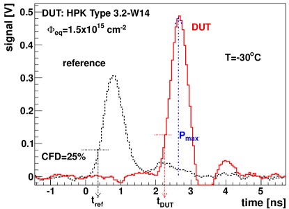
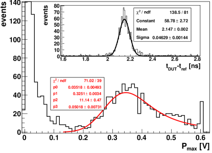
A typical event is shown in Fig. 2a. The timing is determined from the time difference of both signals crossing the threshold. A constant fraction discrimination was used, with the trigger occurring at the time where the signal reached 25% of its maximum. The maximum of the signal response was taken as the measure of the charge. With fast amplifiers the integral of the current pulse is more commonly used, but for short pulses in thin devices the difference is practically negligible. The spectrum of collected charge for a given device was fitted with a convolution of Gaussian and Landau function and the most probable value was taken as collected charge (see Fig. 2b). The measured charge () was converted to absolute charge from unirradiated sensor measurements in a calibrated system using slow electronics [12].
The time resolution of the system was obtained as a standard deviation () of the distribution . A typical distribution and a Gaussian fit to it is shown in the inset of Fig. 2b. The resolution of the reference detector was calibrated before and was ps. The time resolution of the investigated detector is then obtained as
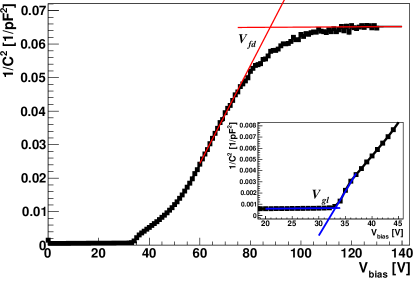
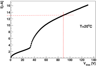
CV/IV measurements were taken in the probe station at C and kHz using Keithley 6517 for voltage source and precise current meter and LCR meter HP4263B. The guard ring was grounded during the measurements. An example of and extraction is shown in Fig. 3a and a corresponding leakage current at in Fig. 3b.
 |
 |
| (a) | (b) |
4 Annealing of the gain layer doping concentration
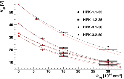
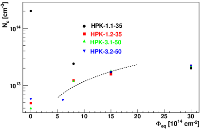
The dependence of on fluence immediately after irradiation (0 min) and after 80 min of annealing at 60∘C is shown in Fig. 4a. Assuming that is proportional to the , its dependence on fluence can be parameterized as
| (4) |
The fits of Eq. 4 to the measured data are also shown and the obtained removal constants are gathered in Table 2. Annealing impacts the gain layer in a moderate way, but even small changes can lead to a substantial impact in gain operation mode as will be discussed later.
 |
 |
| (a) | (b) |
The difference in removal constants for different samples can be attributed to the different doping levels of the various samples and to the shapes of the doping profiles. This information is not revealed by the producer, but the effective doping profiles extracted from C-V reveal a deeper p+ layer for HPK-3.2-50 than for HPK-3.1-50.
| HPK-1.1-35 | HPK-1.2-35 | HPK-3.1-35 | HPK-3.2-35 | |
|---|---|---|---|---|
| cm | 4.50.3 | 3.90.3 | 4.50.3 | 3.30.2 |
| cm | 4.90.3 | 4.20.3 | 4.80.3 | 3.70.3 |
The depends on time after irradiation. A change relative to is shown in Fig. 4b. It seems that the relative change becomes larger with fluence, but doesn’t depend on the sample type. The data for all samples at a given fluence were therefore fitted with
| (5) |
where represents the fraction of effective dopants that change in time and the time constant for the process. The results of the global fit with and to the all the data at a given fluence are shown in Table 3. The increase of the with fluence is evident and amounts to a change in of more than 2 V at cm-2 for HPK-3.2-50. This has an important impact on device performance as will be shown later.
| cm | 8 | 15 | 30 |
|---|---|---|---|
| [min] |
The time constants for different fluences were found to be compatible with an average of min.
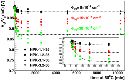
In order to determine the dynamics of these changes at lower temperatures a set of sensors of type HPK-3.2-50 were also annealed at C, which enabled the extraction of the activation energy for the process and thus allow scaling to temperatures close to operation temperatures. The comparison of annealing for C and C is shown in Fig. 5. The fit of Eq. 5 for to the measured data is also shown. The time constants for all three fluences were found comparable for each temperature, yielding an average over the fluences of min and . The fraction of annealed seems to be the same for both temperatures and is in accordance with the given in Table 3. It is therefore reasonable to assume that would be the same also at other annealing temperatures.

As a process governed by thermal energy the Arrhenius relation can be used to determine the activation energy ()
| (6) |
where is the Boltzmann constant. The activation energy eV was obtained. Although uncertainties are large, it allows the scaling to operational temperature of LGADs at HL-LHC years, so annealing is effectively frozen during the yearly operation period.
5 Annealing of the bulk doping concentration and generation current
5.1 Bulk doping concentration
The evolution of the effective doping concentration in the bulk is usually dominated by the deep defects, as the high resistivity silicon is normally used. Apart from the influence of the bulk on the electric field, the bulk generation current is the major source of the leakage current. The effective doping concentration in the bulk was measured as
| (7) |
where is permitivity of Si, permittivity of vacuum, elementary charge, active thickness of the device and the width of the gain layer. The latter is not precisely known, but is around 2 m. The choice of has a marginal impact on . Eq. 7 implies a constant space charge, an assumption that proved fairly accurate for neutron irradiated sensors over past decades. The small thickness of the devices allowed for accurate determination of at relatively large fluences, which is not possible for thicker sensors. On the other hand, mobile impurities, mostly oxygen, can migrate from the substrate and influence the properties of the bulk. For the investigated fluences the decrease in was such that, except for HPK-3.2-50, there was no gain at full depletion of the detector, which only appeared at . Therefore, at voltages close to there was no enhanced hole concentration in the bulk originating from the gain layer.
 |
 |
| (a) | (b) |
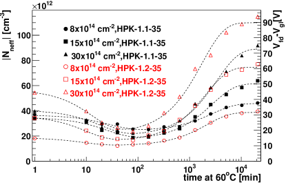
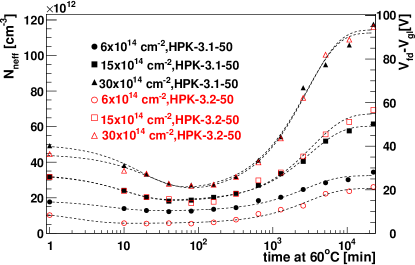
The evolution of the for all the investigated sensors is shown in Figs. 6. The sensors differ in initial bulk resistivity which can be clearly observed in the evolution. The initial boron removal is not yet completed for HPK-1.1-35 at cm-2 (Fig. 6a), hence its minimum in time is larger than that of the other two fluences. The fits of the Hamburg model (Eqs. 2,3) to the all the measured results are also shown and a good description can be observed. The model parameters for the samples in Table 1 are listed in Table 4.
| cm | [ cm-3] | cm | [min] | cm-1] | [min] | |
|---|---|---|---|---|---|---|
| HPK-1.1-35 | 8 | |||||
| HPK-1.1-35 | 15 | |||||
| HPK-1.1-35 | 30 | |||||
| HPK-1.2-35 | 8 | |||||
| HPK-1.2-35 | 15 | |||||
| HPK-1.2-35 | 30 | |||||
| HPK-3.1-50 | 8 | |||||
| HPK-3.1-50 | 15 | |||||
| HPK-3.1-50 | 30 | |||||
| HPK-3.2-50 | 6 | |||||
| HPK-3.2-50 | 15 | |||||
| HPK-3.2-50 | 30 |
The dependence of stable damage on equivalent fluence is shown in Fig. 7. Apart from HPK-1.1-35, the resistivity of samples was high enough for the initial acceptor concentration to be less important. Assuming that the acceptors were completely removed for those samples by irradiation down to the lowest fluence, and excluding the highest fluence point where the saturation of stable damage was earlier observed [14], the slope showed the result to be cm-1, which is somewhat lower than cm-1 measured for detectors at standard thickness irradiated to fluences cm-2 [5].
It has been observed before that thin sensors can have different damage parameters [15] also depending on properties of the support wafer. Introduction of defects that reverse anneal () were found to be smaller, while the time constants ( min) were found to be longer than in standard FZ silicon, but both roughly compatible with those in oxygenated silicon detectors. The short term annealing results are compatible with previous measurements in standard silicon detectors with an introduction rate of cm-1 and annealing times of min, but the uncertainty is rather large. It is worth mentioning that at low the relative uncertainty in determination becomes larger.
At bias voltages high enough for charge multiplication the free hole concentration in the bulk increases which decreases the negative space charge in irradiated detectors. The dependence of traps’ occupancy on free hole concentration was studied by free hole injection through continuous illumination of the surface with red light [16]. The concentration of free holes in the LGAD bulk can be estimated from the leakage current (). As will be shown in the next section currents of few A are measured at high bias voltages and -30∘C. Assuming that holes contribute dominantly to the leakage current for high gain (hole contribution ) the free hole concentration () is given by
| (8) |
where cm/s is saturation velocity of the holes and cm2 is the surface of the detector. The concentration of free holes is therefore in the order of cm-3 for A. Such a concentration influences the space charge, but it still remains negative in the bulk [16]. The effective doping concentration calculated with Eqs. 2, 3 and parameters from Table 4 set the upper limit for the negative space charge inside the detector bulk.
 |
 |
5.2 Generation current
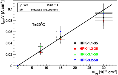
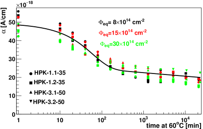
The generation current’s dependence on fluence for the standard annealing point is shown in Fig. 8a. The linear increase with fluence can be observed with the slope cm-1, which is lower than cm-1 commonly used. Although this is a non-negligible difference a combination of several uncertainties, foremost temperature, and fluence, can be a reason for it. The currents normalized to volume and fluence, so called leakage current damage constant , are shown in Fig. 8b. The model used in [17] was fit to the data for all samples, excluding the points for the lowest fluences of 50 m devices which showed some gain already at
| (9) |
The free parameters obtained are gathered in the Table 5.
| cm-1] | cm-1] | cm-1] | [min] |
|---|---|---|---|
The data are in reasonable agreements with previously measured results. The reduction of generation current with time can be exploited for reduction of the power consumption in operation, particularly as after completed annealing of the gain layer the charge collection is unaffected by any further annealing as described in the next section.
6 Annealing effects on timing and charge collection measurements
The ultimate benchmark of the annealing influence on the operation of LGADs is its impact on charge collection and timing resolution. Studies made within ATLAS-HGTD showed that 50 m thick devices outperform 35 m thick ones, due to larger deposited charge, smaller capacitance and less steep increase of charge with bias voltage close to the operation point. Therefore annealing studies in this paper concentrated on HPK-3.1-50 and HPK-3.2-50.
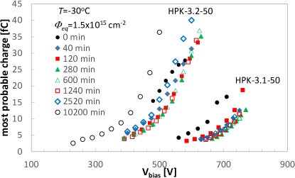
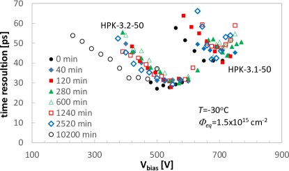
Fig. 9a shows the charge collection (CC) for both sensors after cm-2. There is an obvious difference in CC which is due to a different gain layer profile, both in profile depth and dose. The annealing has little effect, except for the measurement point before any intentional annealing (), which showed significantly larger charge at given voltage than at other annealing points up to 2520 min. This is in agreement with annealing of . Assuming m, the difference of 1 V in roughly transfers to 50-25 V difference in operational voltage to get the same electric field in the gain layer, and hence the same amount of charge. At very large annealing times of min we noticed a much better performance in CC for HPK-3.2-50 with an indication of increase already at 2520 min. We had two parallel detectors and both showed the same behavior. Such a behavior was also observed with ATLAS strip detectors where substantial increase of charge occurred only after min annealing [18, 19]. This improvement can be attributed to a larger impact of the bulk on electric field in the gain layer as described in the introduction.
The timing measurements for both detectors are shown in Fig. 9b. The HPK-3.2-50 shows superior performance reaching time resolution of 30 ps. The performance at different annealing times is in line with the one observed in CC. At the highest voltages the time resolution deteriorates due to the increase of noise, which leads to the increase of jitter. The increase of noise was attributed to the measurements with a floating guard ring and the noise disappeared at later measurements with a grounded guard ring.
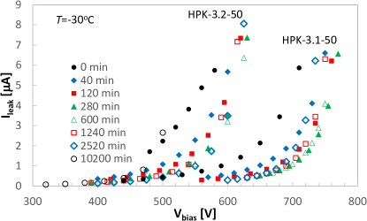
The leakage current measurements for these detectors are shown in Fig. 9c. Although the sum of bulk and guard current is shown the contribution of the latter is usually much smaller. The current decreases with annealing due to decrease of as the gain remains roughly constant except before any intentional annealing and after very long annealing times.
 |
 |
| (a) | (b) |
(c)
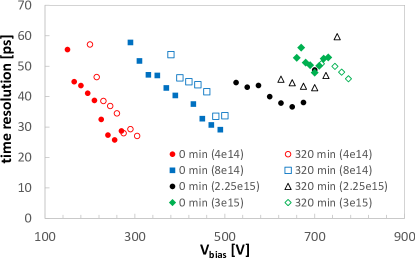
The annealing studies at smaller and larger fluences than cm-2 show the same behavior (see Fig. 10a). As most of the studies done so far were after 80 min annealing, it makes sense to compare the performance of annealed sensors with the one immediately after irradiation. Such a comparison is shown in Fig. 10b. It is clear that the bias voltage difference required for collection of e.g. 10 fC (dashed line) between 0 and 320 min annealing time increases slightly with fluence up to the cm-2, which is in agreement with the increase of with fluence. At the maximum fluence shown the voltage required for multiplication is already so high that it comes close to the breakdown, where the bulk multiplication starts to take place and this relation breaks down. It is therefore clear that the standard annealing point for most LGAD studies so far presents a conservative estimate of their timing and charge collection performance.
 |
 |
| (a) | (b) |
(c)
The time resolution at different fluences is in accordance with charge collection measurements (see Fig. 10c). The resolution decreases steadily with fluence from 27 ps at cm-2 to around 50 ps at cm-2.
6.1 Qualitative explanation of observed results
The effects of initial short term and long term annealing are best illustrated by the calculated electric field for HPK-3.2-50 detector irradiated to cm-2. As shown in Fig. 9a around 20 fC is collected at different annealing stages and bias voltages; 480 V after min, 510 V at 0 min and 570 V after 280 min. The difference originates from a different electric field in the gain layer due to both and . As the detector is always highly over-depleted with drift velocity close to saturated, the gain should depend on the electric field in the gain layer only. The electric field calculated with the approximation of constant doping concentration in two regions with abrupt transition between them is shown in Fig. 11. The values of () and as measured at different annealing stages in this work were used. Although the electric field differs significantly in the bulk it is identical in the gain layer, which validates equal charge measured. This illustrates that although it can significantly impact the electric field in the gain layer.

7 Conclusions
Both bulk and gain layer properties change with time after irradiation. The gain layer effective dopant concentration was found to decrease exponentially with time after the irradiation with time constant of around 50 min at 60∘C and 650 min at 40∘C, yielding the estimation of activation energy of 1.15 eV. Thus, the effective doping concentration in the gain layer won’t anneal until the yearly technical stops at HL-LHC. The relative fraction of the effective doping concentration in the gain layer that anneals after irradiation increases with fluence from around after cm-2, after cm-2 to after cm-2.
The changes of the bulk doping concentration can be well described by the Hamburg model. The short term and long term annealing have introduction rates cm-1 and annealing times tens min, min similar to those observed before in oxygen rich silicon detectors. The introduction of stable acceptors was difficult to estimate as the number of fluences was not enough to accurately model it, but it seems to be compatible with previous measurements. The annealing of generation current exhibit the same behavior as in standard detectors and follows the NIEL prediction.
Somewhat larger doping concentration in the gain layer immediately after irradiation, leads to higher charge collection and better timing resolution at a given voltage, offsetting the operational voltage by 50-100 V in the entire fluence range with respect to that at after standard annealing. However, after few tens of minutes at 60∘C the performance remains largely unaffected up to around thousand minutes. At very large annealing times of min a sizable improvement in charge collection and timing was observed for sensors irradiated to cm-2. A simple calculation of the electric field including all measured bulk and gain layer changes in doping concentration validated the charge collection measurements during different annealing stages. Although very long times are probably unpractical for HL-LHC they can be exploited in the case of unplanned events.
The standard annealing point of 80 min at 60∘C where most of the studies were done so far therefore represents a conservative estimate in terms of required operation voltage.
Acknowledgment
The authors acknowledge the financial support from the Slovenian Research Agency ( program ARRS P1-0135 and project ARRS J1-1699 ).
References
- [1] H.F-W. Sadrozinski, A. Seiden, N. Cartiglia, “4D tracking with ultra-fast silicon detectors”, REPORTS ON PROGRESS IN PHYSICS 81(2) 026101, 2018.
- [2] N. Cartiglia et al. , “Beam test results of a 16 ps timing system based on ultra-fast silicon detectors”, Nucl. Instr. and Meth. A 850 (2017) 83.
- [3] G. Pellegrini et al., “Technology developments and first measurements of Low Gain Avalanche Detectors (LGAD) for high energy physics applications”, Nucl. Instr. and Meth. A 765 (2014) 12.
- [4] M. Ferrero et al., “Radiation resistant LGAD design”, Nucl. Instr. and Meth. A 919 (2019) 16.
- [5] G. Lindström et al., “Radiation hard silicon detectors - developments by the RD48 (ROSE) collaboration”, Nucl. Instr. and Meth. A 466 (2001) p. 308.
- [6] G. Kramberger et al., “Radiation effects in Low Gain Avalanche Detectors after hadron irradiations”, JINST Vol. 10 (2015) P07006.
- [7] ATLAS Collaboration, “Technical Proposal: A High-Granularity Timing Detector for the ATLAS Phase-II Upgrade”, CERN-LHCC-2018-023 (2018).
- [8] CMS Collaboration, “A MIP Timing Detector for the CMS Phase-2 Upgrade”, CERN-LHCC-2019-003 (2019).
- [9] R. Wunstorf, W.M. Bugg, J. Walter et al. “Investigations of donor and acceptor removal and long term annealing in silicon with different boron/phosphorus ratios”, Nucl. Instr. and Meth. A377 (1996) 228.
- [10] M.Ferrero et al., “Radiation resistant LGAD design”, Nucl. Instr. and Meth. A919 (2019) 16.
- [11] L. Snoj, G. Žerovnik, A. Trkov, “Computational analysis of irradiation facilities at the JSI TRIGA reactor”, Appl. Radiat. Isot. 70 (2012) p. 483.
- [12] G. Kramberger et al., “Radiation hardness of thin low gain avalanche detectors”, Nucl. Instr. and Meth. A 891 (2018) 68.
- [13] Z. Galloway et al., “Properties of HPK UFSD after neutron irradiation up to 6e15 n/cm2”, Nucl. Instr. and Meth. A940 (2019) 19.
- [14] G. Kramberger et al., “Modeling of electric field in silicon micro-strip detectors irradiated with neutrons and pions”, JINST Vol. 9 (2014) P10016.
- [15] G. Lindström et al., “Epitaxial silicon detectors for particle tracking—Radiation tolerance at extreme hadron fluences”, Nucl. Instr. and Meth. A 568 (2006) p. 66.
- [16] G. Kramberger et al., “Field engineering by continuous hole injection in silicon detectors irradiated with neutrons”, Nucl. Instr. and Meth. A 497 (2003) p. 440.
- [17] M. Moll, E. Fretwurst, G. Lindstrom et al. ,“Leakage current of hadron irradiated silicon detectors - material dependence”, Nucl. Instr. and Meth. A 426 (1999) 87.
- [18] M. Milovanovic et al. ,“Effects of accelerated long term annealing in highly irradiated n(+)-p strip detector examined by Edge-TCT”, JINST Vol. 7 (2012) P06007.
- [19] L. Diehl et al. ,“Prolonged signals from silicon strip sensors showing enhanced charge multiplication”, APPLIED PHYSICS LETTERS 115 (2019) 223501.