Preliminary Demonstration of a Persistent Josephson Phase-Slip Memory Cell with Topological Protection
Abstract
Superconducting computing promises enhanced computational power in both classical and quantum approaches. Yet, scalable and fast superconducting memories are not implemented. Here, we propose a fully superconducting memory cell based on the hysteretic phase-slip transition existing in long aluminum nanowire Josephson junctions. Embraced by a superconducting ring, the memory cell codifies the logic state in the direction of the circulating persistent current, as commonly defined in flux-based superconducting memories. But, unlike the latter, the hysteresis here is a consequence of the phase-slip occurring in the long weak link and associated to the topological transition of its superconducting gap. This disentangle our memory scheme from the large-inductance constraint, thus enabling its miniaturization. Moreover, the strong activation energy for phase-slip nucleation provides a robust topological protection against stochastic phase-slips and magnetic-flux noise. These properties make the Josephson phase-slip memory a promising solution for advanced superconducting classical logic architectures or flux qubits.
Introduction
A Josephson junction (JJ) consists of a localized discontinuity (weak link) in the order parameter of two superconducting electrodes tinkham_introduction_2004 , where the dissipation-less current ruled by the Cooper pairs transport is controlled by the macroscopic quantum phase difference () across the junction. Weak links are typically realized in the form of a thin insulator, a semiconductor or metallic wire, or a narrow superconducting constriction tinkham_introduction_2004 ; likharev_superconducting_1979 . The junction current-phase relation (CPR) strongly depends on the structural attributes of the constriction, i.e., on how its effective length (, i.e., the distance between the superconducting leads), width (), and thickness () compare with the superconducting coherence length () likharev_superconducting_1979 . In a fully superconducting one-dimensional JJ () the CPR evolves from the single-valued distorted sinusoidal characteristic, typical of the short-junction limit ( Fig. 1a) and of non-superconducting weak links, to the multi-valued function obtained in the long regime (, Fig. 1b) likharev_superconducting_1979 . In the latter scenario, multiple (odd) solutions are available to the system at fixed , and the steady state will depend on the history of . In the specific example of Fig. 1b three solutions are possible for the Josephson current () at close to . Two of them are energetically-stable, they correspond to two local minima in the Josephson energy langer_intrinsic_1967 and are topologically discriminated by the parity of the winding number of the superconducting phase along the wire little_decay_1967 ; strambini_-squipt_2016 which reflects into two opposite directions of petkovic_deterministic_2016 , as indicated in Fig. 1b by the even (red) and odd (blue) branches of . In order to switch between these two stable branches, a slippage of the superconducting phase along the weak link is required. The slippage passes through the third backward solution in the CPR, a metastable state which corresponds to a saddle point in the Josephson energy separating the two stable minima and forming the barrier of a double-well potential. In analogy with the physics of topological insulators, this intermediate metastable state is gapless, and is associated to the formation of a phase-slip center in the middle of the junction langer_intrinsic_1967 ; arutyunov_superconductivity_2008 . The large superconducting condensation energy lost in this gapless center is at the origin of the strong phase-slip energy barrier separating the two topological branches. We take advantage of this topologically-protected double well potential to implement a robust and permanent superconducting memory: The Josephson phase-slip memory (PSM). Differing from similar quantum phase-slip memories mooij_phase-slip_2005 , the geometry of the PSM has been conceived for a deterministic control of the state via an external magnetic field, while stochastic quantum or thermally-activated phase slips are exponentially suppressed. As described below, these events are negligible thanks to the low resistance of the nanowire , where kvirtanen_spectral_2016 .
Results
Implementation of the memory cell
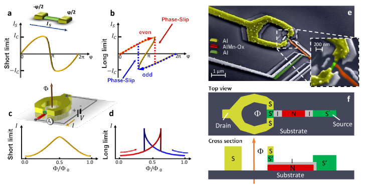
The design of a proof-of-concept PSM requires an architecture enabling the tuning of the superconducting phase and the definition of an efficient readout scheme. To finely control , the JJ is inserted in a superconducting loop, where an external magnetic field gives rise to a total flux () piercing the ring area. Stemming from fluxoid quantization doll_experimental_1961 , the superconducting phase difference across the weak link is given by (where Wb is the flux-quantum) while the phase drop along the loop is negligible (see Methods for details). The phase difference, together with the topological index, determines the amplitude of the superconducting gap in the local density of states (DOS) of the wire virtanen_spectral_2016 , which can be probed by a metallic electrode tunnel-coupled to the middle of the junction, thereby implementing a superconducting quantum interference proximity transistor (SQUIPT) giazotto_superconducting_2010 , as sketched on top of Fig. 1c. As a result, at fixed the amplitude of the tunneling current () flowing through the probing electrode will depend on the even/odd parity of the topological index of the junction codifying the logic [0] and [1] states of the PSM cell (see Fig. 1d). Encoding the memory state in the parity of the winding number is a common feature to all flux-based superconducting memories, including e.g. nano-SQUIDsmurphy_nanoscale_2017 ; ilin_supercurrent-controlled_2021 flux qubitsmooij_superconducting_2006 or kinetic-inductance memories chen_kinetic_1992 from which it shares the low dissipation and high operation speeds. But, differing form the latter approaches, the dynamics of the memory cell here is entirely dominated by the physics of the weak-link. The read out in the SQUPIT is based on a tunneling spectroscopy of the weak-link and the hysteresis in the magnetic flux is not a consequence of an unbalance between the ring and junction inductance but is an intrinsic property of the CPR.
The scanning electron micrograph (SEM) of a representative PSM cell is shown in Fig.1e together with a top-down and cross-section scheme in Fig.1f. Realized through a suspended-mask lithography technique (see Methods for fabrication details) the weak link consists of a one-dimensional Al nanowire (green, = 25 nm and = 90 nm) with a length nm, embedded in a micron-sized 70-nm-thick Al ring (yellow). In addition, a 20-nm-thick normal metal electrode (red, Al0.98Mn0.02) is tunnel-coupled to the center of the wire (with a normal-state tunnel resistance k). To measure the tunneling current, a second Al lead (green) is tunnel-coupled to the normal metal electrode (with a normal-state resistance k) ronzani_phase-driven_2017 . Based on the device structural parameters, we estimate the ratio , where nm is the zero-temperature coherence lengthde_simoni_metallic_2018 , thereby providing the frame of the long-junction regime likharev_superconducting_1979 ; virtanen_spectral_2016 (see Methods for details). Within these geometrical constrains and thanks to the low resistivity of Al (), both quantum and thermally-activated phase slips are negligibly small, with rates Hz (see Methods for more details on the estimate). Notably, the PSM is completely made of aluminum compounds thus ensuring high-quality tunnel barriers and full compatibility of all fabrication steps for industrial scaling.
Magneto-electric response
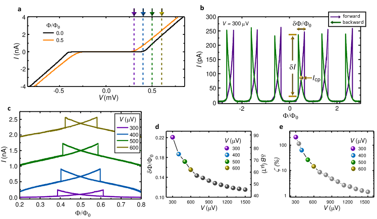
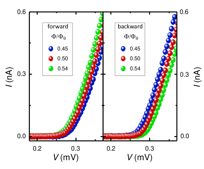
To test the PSM transport properties and assess the operation parameters of the memory cell, we first performed a preliminary magneto-electric characterization at bath temperature mK. Figure 2a shows the current vs voltage characteristics () of a typical device measured at (black curve) and (orange curve). At zero magnetic flux, the quasiparticle tunnel current is suppressed for V due to the presence of two S-I-N tunnel junctions in series and is consistent with the an Al gap of eV for both the read-out lead () and the weak link (). The latter can be modulated by the external magnetic flux giazotto_superconducting_2010 ; ronzani_phase-driven_2017 , showing a reduction of about at (orange line), eV (see also Supplementary Figure 1 for more details). Differently from short-junction SQUIPTs ligato_high_2017 ; ronzani_phase-driven_2017 , the characteristic is not only -periodic, but it is also strongly hysteretic in . This is highlighted in Fig. 2b, where the tunnel current measured at V as a function of increasing (purple trace) and decreasing (green trace) magnetic flux is shown. The forward trace exhibits periodic maxima followed by sudden jumps corresponding to the nucleation of a phase-slip center in the superconducting nanowire likharev_superconducting_1979 ; virtanen_spectral_2016 ; arutyunov_superconductivity_2008 . Accordingly, the backward trace evolves in a totally specular fashion. The evolution of on the bias voltage is shown in Fig. 2c. The hysteresis loop drawn by the back and forth exhibits a reduction of its width () by increasing , as quantified also in Fig. 2d. This trend can be ascribed to a local overheating in the weak link induced by the quasiparticle current flowing through the probing junction which enlarges tinkham_introduction_2004 thereby deviating the CPR towards the single-valued non-hysteretic form likharev_superconducting_1979 ; virtanen_spectral_2016 . The relative separation between the two branches can be quantified by a parameter () defined as the ratio between the current drop at the phase-slip transition and the current at the hysteresis crossing point, , where n is an integer odd number. A large improves the visibility of the PSM logic states. Similarly to , the increase of induces a monotonic reduction of , as shown in Fig. 2e.
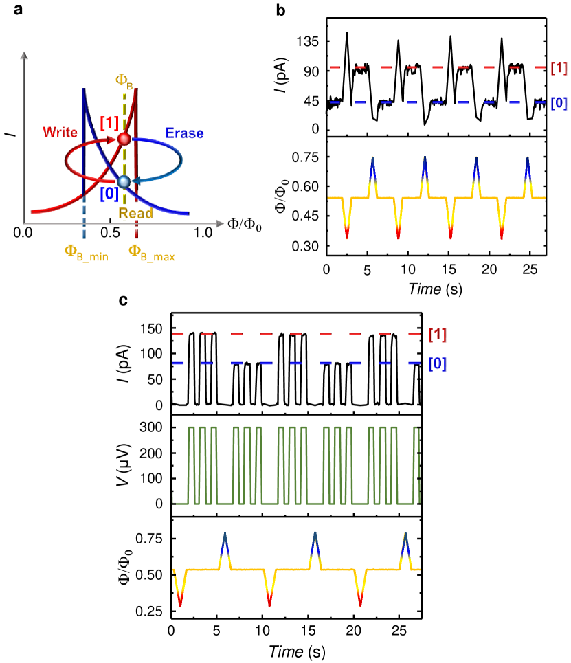
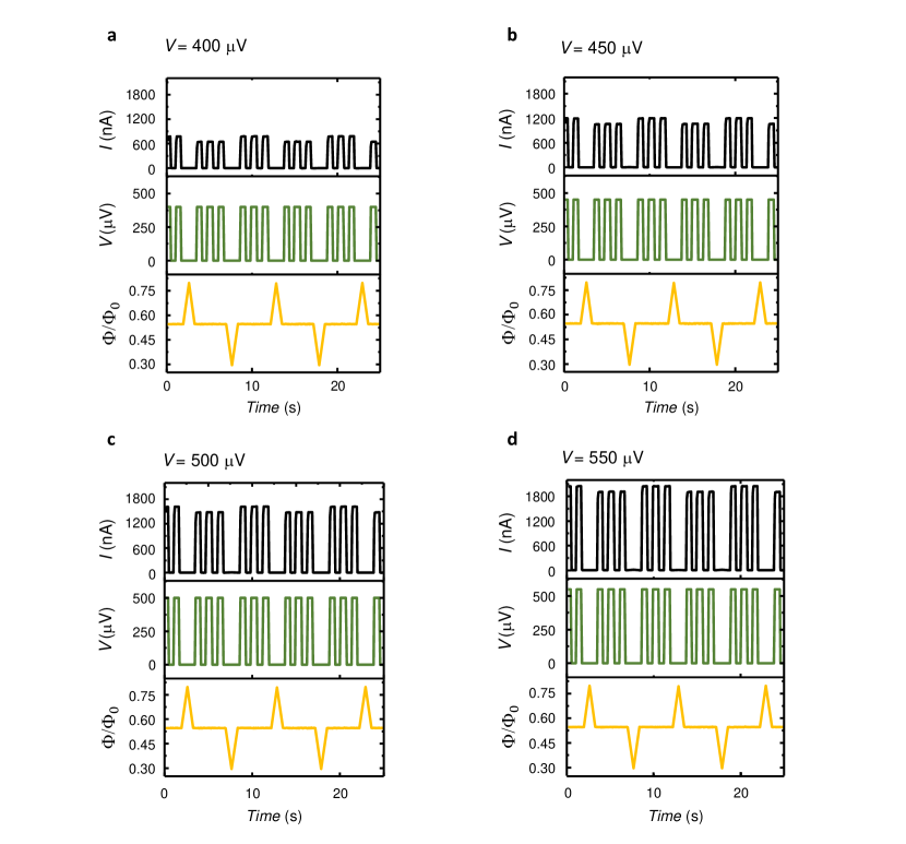
Memory operation with DC readout
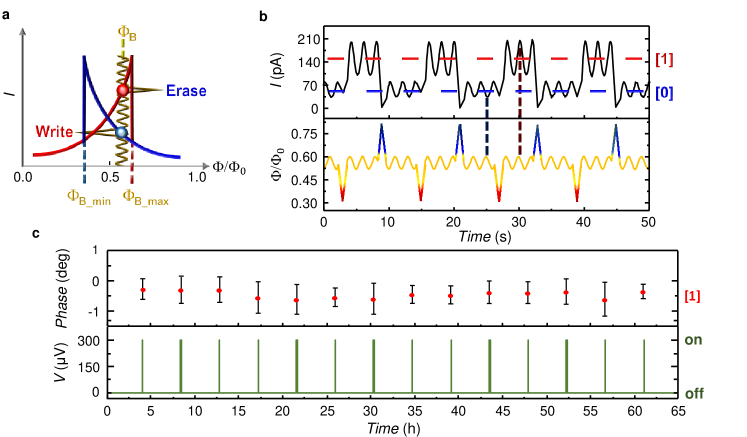
The typical operation cycle of the PSM memory cell is sketched in Fig. 3a. A bias flux () is required to access the multi valued state enclosed within the hysteretic domain (). Writing (erasing) operations are performed by lowering (increasing) the total flux below (above) the hysteretic domain by means of short pulses. As a consequence, the parity of the topological index switches between odd and even and the tunneling current between low and high current state. Figure 3b shows a real-time writing/erasing operation in the continuous read-mode, i.e., with a fixed a bias voltage V. The bias flux is set at , just above the crossing-point of the hysteresis to avoid degeneracy in the current amplitude (see Fig. 2c). The memory is then initialized in the [0] state corresponding to a current pA. By applying a negative flux pulse down to , the PSM logic state suddenly transits to [1] as detected by the current jump to pA. Conversely, the logic state [0] is recovered via a positive erasing flux pulse up to . The device unequivocally shows the typical behavior of a memory cell upon many erasing/writing cycles. From the real-time characteristic is possible also to quantify the energy required for the writing/erasing operations. This can be estimated from the energy difference of the system in the two flux configurations that can be simplified in , where is the kinetic inductance of the JJ mooij_phase-slip_2005 . In our experimental configuration, the estimated energy is eV, this number is consistent with the predictions for the energy of the topological barrier virtanen_spectral_2016 . Notably, differing from conventional flux-based superconducting memories, the inductance of the PSM ring is not relevant for the device which can be made negligibly small without any loss of hysteresis or functionality. This allows the miniaturization of the PSM that could be further operated with a flux generated by supercurrents directly injected in a small portion of the superconducting ring enrico_-chip_2019 therefore eliminating the requirement of an external magnetic field but with the disadvantage of an additional feed line integrated in the device.
The ability of a memory cell to retain the data even when the power is temporarily turned off is called non-volatility, which, even if not essential for a RAM memory, it is an adding value for energy saving and data storage. The PSM requires two power sources: one to generate the bias flux and one for the read-out signal. The former was provided by an external superconducting magnetic controlled by a current source, then power dependent. To overcome this limitation could also be generated by a permanent dissipationless superconducting coil as well as a metallic ferromagnetic layer buried in the semiconducting substrate or by directly employing a ferromagnetic insulator as dielectric substratestrambini_revealing_2017 ; de_simoni_toward_2018 . Alternatively, a proper phase bias might be generated with an additional ferromagnetic pi-junction ryazanov_coupling_2001 inserted in the ring or through a phase-battery strambini_josephson_2020 . The read-out voltage is only required to probe the resistance state of the PSM. As demonstrated in Figure 3c, temporarily and repeated measures of both logic states do not affect the stored data with a readout dissipation as low as fW and fW for logic state [0] and [1], respectively, and only limited by the noise of the current amplifier. This low dissipated power combined with the intrinsic cutoff time ps estimated from the RC circuit of the tunnel junctions (see Methods for details) yields a predicted tiny energy required per bit readout eV and eV. These values were only estimated, and stem from the severe bandwidth limitations of the cryogenic filters. Similarly to rapid single flux quantum, the writing/erasing process is expected with a switching time of ps which is typical for small superconducting loops golod_single_2015 ; zhao_compact_2018 ; ryazanov_magnetic_2012 . The PSM speed is therefore expected to be on par with current state-of-the-art superconducting memories both in the reading and in the writing/erasing process vernik_magnetic_2013 ; gingrich_controllable_2016 ; golod_single_2015 ; madden_phase_2018 ; zhao_compact_2018 .
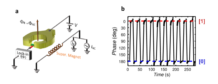
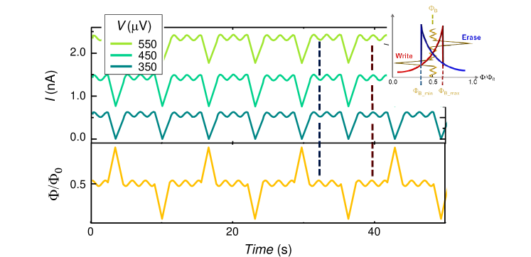
Memory robustness and operation with AC readout
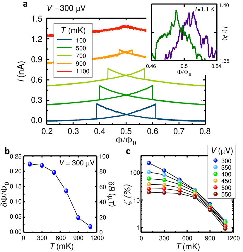
The robustness of the PSM against flux fluctuations is tested by superimposing to the working biasing flux a sizable sinusoidal signal (, see Fig. 4a). The PSM shows optimal stability with respect to flux oscillations, as shown in Fig. 4b for V and . The memory preserves the stored state and keeps the readout value of the two logic states well separated for fluctuations , then of the hysteretic domain of the memory , at least. Interestingly, thanks to the opposite sign of the magnetoconductance of PSM in the two topological states (visible for instance in Fig. 2b and c), the AC flux modulation induces an AC response in the tunneling current which acquires a shift when switching between the two logic states [0] and [1]. This phase shift provides a complementary and efficient method to probe the parity of the JJ winding number, which is not affected by the position of within the hysteretic domain, or by the low visibility of the DC readout signal (see also Supplementary Figure 4 and 5 for more details). This allows to operate the memory cell also in the degenerate point , where the energies of the [0] and [1] states are equal, a basic condition to implement a phase-slip qubit mooij_phase-slip_2005 ; mooij_superconducting_2006 . Therefore, the PSM provides an alternative low-frequency method for the qubit readout. With the phase-based readout the persistency of the PSM have been tested up to almost three days, as shown in Figure 4c. The memory is initialized to logic state [1], and the readout is performed every 4 hours. No sign of signal degradation has been observed even after days of measurement confirming the vanishing phase-slip rate (Hz) as estimated from our parameters virtanen_spectral_2016 ; arutyunov_superconductivity_2008 (See Methods for details on the estimate). As a consequence, the memory error rate expected for quantum and thermally-activated phase slips is infinitesimally small and errors can be generated only by large magnetic-flux fluctuations () of the driving magnetic flux. The other source of error that might degrade the memory state is the reading current that could switch the memory via inductive coupling to the ring or by quenching the superconductivity of the weak-link, as commonly happen for superconducting kinetic inductance memoriesilin_supercurrent-controlled_2021 . Differing from the latter, the high resistance of the probing tunnel barrier strongly limits the reading current to nA, then much smaller than the current required for switching (mA)enrico_-chip_2019 and the critical current of the weak-link (A for an Al nanowirebours_unveiling_2020 ). This makes also the error rate during readout operation negligible. High temperature can degrade the performance of PSM by increasing tinkham_introduction_2004 thereby lowering the JJ effective length, and driving the nanowire junction towards the non-hysteretic single-valued CPR occurring for likharev_superconducting_1979 ; troeman_temperature_2008 . In addition, thermal activation can substantially increase the phase-slip rate in the vicinity of the transition that is at and ) virtanen_spectral_2016 . Figure 5a shows the evolution of the hysteresis loop at several bath temperatures (). The hysteresis progressively fades out by increasing , but persists up to K, which corresponds to of the nanowire critical temperature, with reduced to the of the base temperature value (see Fig. 5b). Consequently, also the contrast lowers by increasing , as shown in Fig. 5c. Still, the visibility of the hysteresis loop at high-temperatures demonstrates the strength of the PSM with a substantial protection of the topological state even in the presence of a sizable amount of hot quasi-particles little_decay_1967 . Although the low achieved at high temperature degrades the robustness of the memory with respect to flux-noise, it also allows to write the memory cell with smaller fluxes for a total cost of operation down to meV.
Discussion
In summary, we have envisioned and demonstrated an original persistent Josephson phase-slip single memory cell which takes advantage of fluxoid quantization to codify two logic states in the topological index of the system, i.e., the parity of the superconducting winding number strambini_-squipt_2016 . Differing from conventional superconducting loops ilin_supercurrent-controlled_2021 ; murphy_nanoscale_2017 ; zhao_compact_2018 , here the separation between the two topological states is provided by the large phase-slip barrier, which is unique to long superconducting JJs little_decay_1967 ; virtanen_spectral_2016 . Moreover, its operation mechanism is completely independent of the size or inductance of the superconducting loop thus allowing device miniaturization only limited by fabrication capabilities. The memory exploits conventional superconductors thereby avoiding the use of complex ferromagnetic metals typical of present superconducting memories ryazanov_magnetic_2012 ; gingrich_controllable_2016 ; baek_hybrid_2014 ; golod_single_2015 ; madden_phase_2018 ; vernik_magnetic_2013 . Notably, the performances of the PSM are competing with state-of-the-art superconducting memories with an extremely low energy dissipation per bit operation ( J and J for readout and write, respectively) and high operation speed (up to ps and ps for readout and write, respectively). Thanks to the topological protection, the PSM shows endurance, persistence, and high-temperature operation (up to K), only limited by the Al critical temperature. The use of vanadium ligato_high_2017 or niobium jabdaraghi_low-temperature_2016 , therefore, could extend the memory operation above liquid He temperature, and further promote miniaturization thanks to the lower coherence length of these metals respect to Al.
In addition, our phase-based read-out scheme ensures protection against magnetic flux fluctuations, and provides ideal visibility in all the operation ranges. In fact, despite being intrinsically slower than conventional methods (high-speed lock-in amplifiers reach nowadays a clock frequency of about MHz), the phase-based readout can be a valuable approach for the readout of phase-slip qubits. Furthermore, scalability to large arrays of PSM cells might be designed by taking advantage of the well known architectures employed for transition edge sensors, since both devices are based on a precise resistance measurement. In particular, frequency domain multiplexing or microwave resonators together with SQUID amplifiers ullom_review_2015 could be used for the selective read-out of each PSM composing the total memory.
Sneak currents can be avoided by employing strongly non-linear resistors between each single memory unit, such as superconductor/insulator/normal metal/insulator/superconductor Josephson junctions. Integrating superconducting current feed lines in the ringenrico_-chip_2019 will allow to scale also the write procedure with the additional cost of wiring complexity. Yet, the presence of independent write and read lines, with the former characterized by a low impedance, increases stability against perturbations of the read current and might simplify the integration of the PSM with existing superconducting logic elements including rapid single flux quantumgolod_single_2015 ; zhao_compact_2018 ; ryazanov_magnetic_2012 , reciprocal quantum logic Herr , quantum flux parametrons Hosoya , Josephson field-effect transistors Doh , and gate-controlled cryotrons de_simoni_metallic_2018 ; Paolucci1 ; Paolucci2 . Yet, the strong topological protection and stability observed in the PSM make our approach promising in light of the implementation of phase-slip flux qubits mooij_phase-slip_2005 ; mooij_superconducting_2006 and quantum memories.
Methods
Device fabrication details.
The hybrid memory cells were realized by shadow-mask lithography technique. The suspended resist-mask was defined by electron-beam lithography (EBL) onto a SiO2 wafer. All metal-to-metal clean interfaces, and metal-to-oxide barriers were realized in an ultra-high vacuum (UHV) electron-beam evaporator (EBE) with a base pressure of 10-11 Torr equipped with a tiltable sample holder suitable for multi-directional depositions. In order to obtain wire/ring transparent interfaces, which is crucial for the device operation, the use of the same material is strongly recommendedronzani_phase-driven_2017 . Therefore, the nanowire and the ring of the PSM were realized with aluminum. Furthermore, the Al film evaporation is relatively simple, and its high-quality native oxide allows the realization of good tunnel barriers through oxygen exposure at room temperature. At first, 15 nm of Al0.98Mn0.02 were evaporated at an angle of -18∘ to realize the normal metal electrode. Subsequently, the sample was exposed to 60 mTorr of O2 for 5 min in order to form the thin insulating AlMnOx layer. Next, the sample holder was tilted to 10∘ for the deposition of 20 nm of Al realizing the SQUIPT nanowire (length = 400 nm, width nm and thickness nm) and the superconducting electrodes. Finally, a thicker layer of Al ( nm) was evaporated at 0∘ to realize the superconducting loop of circumference m, and average width nm.
Magneto-electric characterization.
The magneto-electric characterization of the samples was performed at cryogenic temperatures in a 3He-4He dilution refrigerator (Triton 200, Oxford Instruments) equipped with RC-filters of resistance 2k. The out-of-plane magnetic field was applied via a superconducting magnet driven by a low-noise current source (Series 2600, Keithley Instruments). The DC measurements were performed in a two-wire voltage-bias configuration through a low-noise voltage DC source (GS200, Yokogawa) coupled with a room-temperature current preamplifier (Model 1211, DL Instruments) (see Fig. 1-c). The AC characterization was performed via a combination of DC bias and low-frequency lock-in technique. A DC bias voltage () was applied to the device. A current given by the sum of a DC and AC sinusoidal modulation energized the superconducting magnet. The read-out current oscillations induced by variation of , and the phase of the signal (with respect to the flux oscillations) were recorded by a lock-in amplifier (SR830, Stanford Research Systems). Further details on the readout scheme can be found in the note 5 of the Supplementary Information.
Device parameters.
Based on the device structure, we estimate the zero-temperature nanowire coherence length = nm, where is the reduced Planck constant, cm2s-1 is the diffusion coefficient, and 200 eV is the zero-temperature gap in Al. The nanowire critical temperature is K, where is the Boltzmann constant. At low temperature, the ratio confirming the frame of the long JJ regime for the PSM.likharev_superconducting_1979 . The single-valued CPR limit (achieved for nm) is reached at temperature K likharev_superconducting_1979 , where nm is the nanowire mean free path, and m/s is the Fermi velocity of Al.
The kinetic inductance () of a long JJ depends on the geometry and superconducting properties of the nanowirevirtanen_spectral_2016 . In our case, at mK it takes the value pH meservey_measurements_1969 . The nanowire normal-state resistance is given by , where S m-1 is the Al film conductance (with J-1m-3 the density of states at the Fermi energy of Al). Analogously, the ring total inductance (including both the geometric and kinetic contributions) takes the value 1 pH ronzani_phase-driven_2017 (with normal-state resistance ). The contribution of the ring to the total inductance of the SQUIPT yields a screening parameter . The small cannot account for the hysteretic behavior of the PSM, which stems, differently, from the long-junction regime of the Josephson nanowire. The writing/erasing time () is mainly due to the time required to polarize the SQUIPT with the external flux. It is given by 1 ps, where and are the total inductance and resistance of the SQUIPT, respectively. The read-out time () is predominantly limited by the characteristic time of the two tunnel barriers, ps, where ps is the characteristic time of the first tunnel junction, and ps is the time constant of the second junction. The junctions capacitances ( fF and fF) are estimated from the area and the typical specific capacitance of AlOx tunnel barriers fF/m2
Phase-slip rates
Stochastic phase-slips are possible via quantum tunneling and thermal activation. They scale exponentially with the phase-slip barrier, the former with while the latter with . Both of them are small for (where ), as demonstrated in the following. The quantum phase-slip rate is mooij_phase-slip_2005 :
| (1) |
where THz is the quantum phase-slips attempt frequency. With the parameters of our experiment we obtain the negligibly small Hz. Thermally activated phase-slips rate reads arutyunov_superconductivity_2008 :
| (2) |
where is the free energy difference of the potential barrier and is the attempt frequency. In the temperature range of the experiment , is expected to be even smaller then . As an example, at mK the attempt frequency is THz and Hz. From these equations is possible to see that is relevant only at temperature very close to Tc.
Data Availability
The data that support the findings of this study are available from the corresponding author upon reasonable request.
Acknowledgements
The authors acknowledge M. Cuoco and P. Virtanen for fruitful discussions. N.L., E.S., and F.G. acknowledge partial financial support from the European Union’s Seventh Framework Programme (FP7/2007-2013)/ERC Grant No. 615187- COMANCHE. N.L., E.S., and F.G. were partially supported by EU’s Horizon 2020 research and innovation program under Grant Agreement No. 800923 (SUPERTED). The work of F.P. was partially supported by the Tuscany Government (Grant No POR FSE 2014-2020) through the INFN-RT2 172800 project. The authors acknowledge the European Union (Grant No. 777222 ATTRACT) through the T-CONVERSE project.
Author contributions
E.S. and F.G. conceived the experiment. N.L. fabricated the samples with inputs from F.P.. N.L. and E.S. performed the measurements. N.L. analyzed the experimental data with inputs from E.S. and F.G.. All the authors discussed the results and their implications equally at all stages and wrote the manuscript.
Competing Interests
The authors declare no competing interests
References
- (1) Tinkham, M. Introduction to superconductivity. Dover books on physics (Dover Publ, Mineola, NY, 2004), 2. ed edn.
- (2) Likharev, K. K. Superconducting weak links. Rev. Mod. Phys. 51, 101–159 (1979).
- (3) Langer, J. S. & Ambegaokar, V. Intrinsic Resistive Transition in Narrow Superconducting Channels. Phys. Rev. 164, 498–510 (1967).
- (4) Little, W. A. Decay of Persistent Currents in Small Superconductors. Phys. Rev. 156, 396–403 (1967).
- (5) Strambini, E. et al. The -SQUIPT as a tool to phase-engineer Josephson topological materials. Nat Nano 11, 1055–1059 (2016).
- (6) Petković, I., Lollo, A., Glazman, L. I. & Harris, J. G. E. Deterministic phase slips in mesoscopic superconducting rings. Nat Commun 7, 1–7 (2016).
- (7) Arutyunov, K. Y., Golubev, D. S. & Zaikin, A. D. Superconductivity in one dimension. Physics Reports 464, 1–70 (2008).
- (8) Mooij, J. E. & Harmans, C. J. P. M. Phase-slip flux qubits. New J. Phys. 7, 219–219 (2005).
- (9) Virtanen, P., Ronzani, A. & Giazotto, F. Spectral Characteristics of a Fully Superconducting SQUIPT. Phys. Rev. Applied 6, 054002 (2016).
- (10) Troeman, A. G. P. et al. Temperature dependence measurements of the supercurrent-phase relationship in niobium nanobridges. Phys. Rev. B 77, 024509 (2008).
- (11) Doll, R. & Näbauer, M. Experimental Proof of Magnetic Flux Quantization in a Superconducting Ring. Phys. Rev. Lett. 7, 51–52 (1961).
- (12) Giazotto, F., Peltonen, J. T., Meschke, M. & Pekola, J. P. Superconducting quantum interference proximity transistor. Nat. Phys. 6, 254 (2010).
- (13) Murphy, A., Averin, D. V. & Bezryadin, A. Nanoscale superconducting memory based on the kinetic inductance of asymmetric nanowire loops. New J. Phys. 19, 063015 (2017).
- (14) Ilin, E. et al. Supercurrent-controlled kinetic inductance superconducting memory element. Applied Physics Letters 118, 112603 (2021). Publisher: American Institute of Physics.
- (15) Mooij, J. E. & Nazarov, Y. V. Superconducting nanowires as quantum phase-slip junctions. Nature Phys 2, 169–172 (2006).
- (16) Chen, G., Rosenthal, P. & Beasley, M. Kinetic inductance memory cell. IEEE Transactions on Applied Superconductivity 2, 95–100 (1992). Conference Name: IEEE Transactions on Applied Superconductivity.
- (17) Ronzani, A., D’Ambrosio, S., Virtanen, P., Giazotto, F. & Altimiras, C. Phase-driven collapse of the Cooper condensate in a nanosized superconductor. Phys. Rev. B 96, 214517 (2017).
- (18) De Simoni, G., Paolucci, F., Solinas, P., Strambini, E. & Giazotto, F. Metallic supercurrent field-effect transistor. Nature Nanotechnology 13, 802–805 (2018).
- (19) Ligato, N., Marchegiani, G., Virtanen, P., Strambini, E. & Giazotto, F. High operating temperature in V-based superconducting quantum interference proximity transistors. Scientific Reports 7, 8810 (2017).
- (20) Enrico, E., Croin, L., Strambini, E. & Giazotto, F. On-chip tuning of electrodes quasiparticles population in fully superconducting SQUISETs. arXiv:1901.01248 [cond-mat] (2019).
- (21) Strambini, E. et al. Revealing the magnetic proximity effect in EuS/Al bilayers through superconducting tunneling spectroscopy. Physical Review Materials 1, 054402 (2017).
- (22) De Simoni, G., Strambini, E., Moodera, J. S., Bergeret, F. S. & Giazotto, F. Toward the Absolute Spin-Valve Effect in Superconducting Tunnel Junctions. Nano Letters 18, 6369–6374 (2018).
- (23) Ryazanov, V. V. et al. Coupling of Two Superconductors through a Ferromagnet: Evidence for a Junction. Phys. Rev. Lett. 86, 2427–2430 (2001).
- (24) Strambini, E. et al. A Josephson phase battery. Nature Nanotechnology 15, 656–660 (2020).
- (25) Golod, T., Iovan, A. & Krasnov, V. M. Single Abrikosov vortices as quantized information bits. Nat Commun 6, 1–5 (2015).
- (26) Zhao, Q.-Y. et al. A compact superconducting nanowire memory element operated by nanowire cryotrons. Supercond. Sci. Technol. 31, 035009 (2018).
- (27) Ryazanov, V. V. et al. Magnetic Josephson Junction Technology for Digital and Memory Applications. Physics Procedia 36, 35–41 (2012).
- (28) Vernik, I. V. et al. Magnetic Josephson Junctions With Superconducting Interlayer for Cryogenic Memory. IEEE Transactions on Applied Superconductivity 23, 1701208–1701208 (2013).
- (29) Gingrich, E. C. et al. Controllable josephson junctions containing a ferromagnetic spin valve. Nat Phys 12, 564–567 (2016).
- (30) Madden, A. E., Willard, J. C., Loloee, R. & Birge, N. O. Phase controllable Josephson junctions for cryogenic memory. Supercond. Sci. Technol. 32, 015001 (2018).
- (31) Bours, L., Mercaldo, M. T., Cuoco, M., Strambini, E. & Giazotto, F. Unveiling mechanisms of electric field effects on superconductors by a magnetic field response. Physical Review Research 2, 033353 (2020).
- (32) Baek, B., Rippard, W. H., Benz, S. P., Russek, S. E. & Dresselhaus, P. D. Hybrid superconducting-magnetic memory device using competing order parameters. Nature Communications 5, 3888 (2014).
- (33) Jabdaraghi, R. N., Peltonen, J. T., Saira, O.-P. & Pekola, J. P. Low-temperature characterization of Nb-Cu-Nb weak links with Ar ion-cleaned interfaces. Appl. Phys. Lett. 108, 042604 (2016).
- (34) Ullom, J. N. & Bennett, D. A. Review of superconducting transition-edge sensors for x-ray and gamma-ray spectroscopy. Superconductor Science and Technology 28, 084003 (2015).
- (35) Herr, Q. P., Herr, A. Y., Oberg, O. T. & Ioannidis, A. G. Ultra-low-power superconductor logic. J. Appl. Phys. 109, 103903 (2011).
- (36) Hosoya, M. et al. Quantum flux parametron: a single quantum flux device for Josephson supercomputer. IEEE Trans. Appl. Supercond. 1, 77–89 (1991).
- (37) Doh, Y.-J. et al. Tunable Supercurrent Through Semiconductor Nanowires. Science 309, 272–275 (2005).
- (38) Paolucci, F. et al. Magnetotransport Experiments on Fully Metallic Superconducting Dayem Bridge Field-Effect Transistors. Phys. Rev. Applied 11, 024061 (2019).
- (39) Paolucci, F. et al. Field-Effect Control of Metallic Superconducting Systems. AVS Quantum Sci. 1, 016501 (2019).
- (40) Meservey, R. & Tedrow, P. M. Measurements of the Kinetic Inductance of Superconducting Linear Structures. Journal of Applied Physics 40, 2028–2034 (1969).
Supplementary Information
I Hysteresis in the current vs voltage characteristics
To test the PSM transport properties and highlight the hysteresis in its magneto-resistance, we electrically characterized the device at mK. Figure S1 shows the current vs voltage characteristics () of a typical PSM measured at (blue curve), (red curve) and (green curve) for positive (left) and negative (right) sweeps of the magnetic flux. The tunnel () characteristics reveal a magnetic-flux-induced modulation of the superconducting gap of the Al nanowire (), and hysteric behavior with , showing a maximum reduction of at = and for the forward and backward traces, respectively.
II PSM in continuous read-out configuration for several applied voltage biases
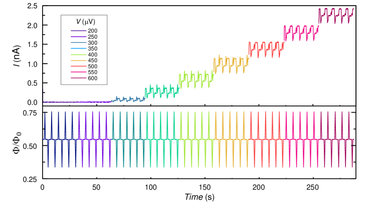
In order to find the optimal operating parameters for the PSM, we performed the writing/erasing operations in the continuous read-mode, i.e., when a bias voltage (V) is permanently applied, varying the values of from 200 V to 600 V, as shown in Fig. S2 at mK. The bias flux is set just above the crossing-point of the hysteresis, namely at . The memory can be written or erased by applying a flux pulse down to or up to , respectively.
The PSM shows the typical behavior of a memory cell with distinct current values for and states for V. By increasing the visibility between the two stored states increases until saturating for the largest biases. This trend is due to local overheating in the weak link induced by the quasiparticle current flowing through the probing junction, which increases thereby deviating the CPR towards the single-valued non-hysteretical form. Finally, we stress that the memory works properly for many bias cycles, confirming the endurance of the PSM cell.
III Non-volatility of the PSM measured at different voltage biases
Here, we study the non-volatility of the PSM. Since the quiescent magnetic flux could be provided by a metallic ferromagnet buried in the isolating substrate or by a ferromagnetic insulator dielectric, the only power source relevant for the PSM is the voltage bias (). Figure S3 shows the non-volatility of the device measured for several values of . Temporarily removing the voltage bias has no effect on the stored data. In fact, the reading voltage is set to only during the readout operation. In addition, the writing, erasing and reading operations have been performed several times without any sizeable outcome change.
IV PSM operation at the degenerate flux
This section is devoted to the study of the properties of the PSM when operated at the degenerate flux , where the two current branches are expected to show the same value. To this end, we bias the device with a constant voltage () while a sinusoidal oscillation of the magnetic flux is superimposed on . Figure S4 confirms that the average values of I[0] and I[1] are indistinguishable. Conversely, the readout current oscillates in reversed phase depending on the stored state. Therefore, the information of the memory state is stored in the phase of the current signal, thus enabling the design of a phase-dependent readout.
V Phase-dependent read-out scheme
The phase-dependent read-out can be realized by means of the experimental setup shown in Fig. S5a. The total magnetic flux is the sum of a constant component (due to the current flowing in the superconducting magnet) and a small sinusoidal component (due to the current ). The PSM is biased with a constant voltage V. The phase of the output current () is measured with a lock-in amplifier with respect to the oscillations. The results are summarized in Fig. S5b. The readout current for state oscillates in phase with the magnetic flux oscillations, while state shows a counter phase (180∘) fluctuation. We note that the device unequivocally shows the typical behavior of a memory cell upon many erasing/writing cycles even for the phase-dependent readout.