Topological valley plasmon transport in bilayer graphene metasurfaces for sensing applications
Abstract
Topologically protected plasmonic modes located inside topological bandgaps are attracting increasing attention, chiefly due to their robustness against disorder-induced backscattering. Here, we introduce a bilayer graphene metasurface that possesses plasmonic topological valley interface modes when the mirror symmetry of the metasurface is broken by horizontally shifting in opposite directions the lattice of holes of the top layer of the two freestanding graphene layers. In this configuration, light propagation along the domain-wall interface of the bilayer graphene metasurface shows unidirectional features. Moreover, we have designed a molecular sensor based on the topological properties of this metasurface using the fact that the Fermi energy of graphene varies upon chemical doping, namely molecular adsorption in our case. This effect induces strong variation of the transmission of the topological guided modes, which can be employed as the underlying working principle of gas sensing devices. Our work opens up new ways of developing robust integrated plasmonic devices for molecular sensing.
Research in topological photonics, inspired by the theory of quantum Hall effect in solid-state physics, has led to the discovery of novel and unique phenomena, such as unidirectional, defect-immune, and scattering-free propagation of light [1, 2, 3, 4, 5, 6], which have the potential to contribute to the development of robust on-chip ultracompact nanophotonic devices. Topological photonic modes could be achieved by gapping out symmetry-protected Dirac cones, for example, through time-reversal symmetry breaking induced by magneto-optical effects under an external static magnetic field, or spatial-inversion symmetry breaking induced by spatially asymmetric perturbations [1, 2, 3]. Currently, a variety of experimental platforms are available for topological photonics, including metamaterials, photonic crystals, and evanescently coupled waveguides and optical-ring resonators [3].
Valley degree of freedom, which is associated to the conduction-band minima (or valence-band maxima) in graphene-like two-dimensional (2D) materials [4], has recently been introduced to photonics [5], too. These materials exhibit nontrivial Berry curvature distribution in the momentum space around each valley, which gives rise to a valley-dependent topological index associated to the integral of Berry curvature around a valley [4]. Furthermore, a domain-wall interface separating two topologically distinct valley photonic crystals can support valley-momentum locked modes localized at the interface, similar to the quantum-valley Hall effect [5]. Until now, valley-Hall photonic modes have been mostly studied in bulk materials, such as photonic crystals [1, 2, 3], being less explored in 2D photonic platforms, including graphene [7]. This 2D material is becoming a promising platform to achieve passive and active topologically protected plasmonic modes [8, 9], due to its high carrier mobility and long relaxation time [10, 11]. Equally important, recent advances in nanofabrication techniques make it possible to achieve graphene based plasmonic nanostructures with particularly complex geometrical configurations[12, 13].
In this paper, we design a bilayer graphene metasurface to realize, to the best of our knowledge for the first time, valley topological plasmonic modes by utilizing a novel mechanism of mirror symmetry breaking between the top and bottom freestanding layers of a graphene metasurface, by horizontally shifting in opposite directions the lattice of holes of the top layer. As such, the symmetry-protected Dirac cones are gapped out and, consequently, a topological nontrivial frequency gap emerges. Furthermore, topologically guided valley modes are observed along a domain-wall interface with respect to which the composite metasurface is mirror symmetric. Our full-wave numerical simulations, based on solving the full set of 3D Maxwell equations via the finite element method, verify that the light propagation along the domain-wall interface shows indeed unidirectional feature. Employing this unique feature of unidirectional propagation and the tunable optical response of graphene, a molecular sensor based on this newly proposed topological metasurface is designed and its sensitivity and functionality are quantitatively characterized.
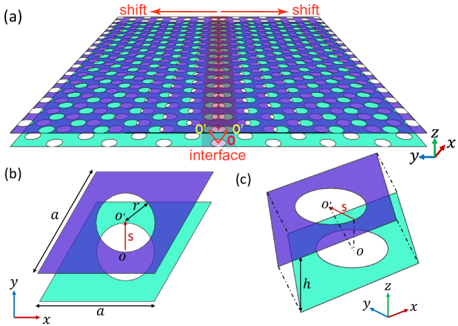
The schematic of the proposed topological bilayer graphene metasurface is shown in Fig. 1. It consists of two freestanding, optically coupled graphene plasmonic crystals with the same unit cell. Note that the conclusions of this study remain qualitatively valid if one assumes that the two graphene layers are separated by a certain dielectric material instead of air, the only changes being of quantitative nature. Moreover, the hole lattice of the left- and right-hand side domains of the top graphene layer are horizontally shifted, in opposite directions and normally onto an interface lying along the -axis, by a certain distance, . Each domain consists of a hexagonal graphene plasmonic crystal with a hole in the unit cell. The top and bird’s-eye views of the unit cell are given in Figs. 1(b) and 1(c), respectively. In this work, we fix the lattice constant , the radius of holes , and the distance between the top and bottom graphene layers .
The optical properties of graphene are described by its electric permittivity, , which is given by Kubo’s formula [11]:
| (1) |
where is the frequency, is the temperature, is the chemical potential, is the graphene thickness, , and , with being the relaxation time. Note that dispersive and dissipative effects are incorporated in our simulations via the frequency-dependent complex surface conductivity of graphene, defined as . In our analysis, and , and we set unless otherwise stated.
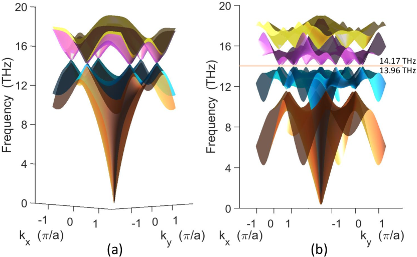
Unlike the case of the mirror-symmetric bilayer graphene metasurface (), in the case of a metasurface with , the frequency maxima and minima are not necessarily located at the high-symmetry points of the first Brillouin zone (FBZ) [14]. Thus, in order to properly identify the frequency band gap, the plasmonic bands of this bilayer graphene metasurface have been evaluated in the entire FBZ and the results are given in Fig. 2 (we have used the Wave Optics Module of COMSOL Multiphysics 5.4). When the distance between the top and bottom graphene layers in Fig. 1(c) is large, the optical near-field coupling between the two layers can be neglected. As a consequence, each graphene layer, which is a plasmonic crystal, possesses decoupled Dirac cones protected by point symmetry group [15]. This is indeed verified by the bands presented in Fig. 2(a), where the Dirac cones located at of each graphene plasmonic crystal perfectly overlap. In order to enhance the optical coupling between the top and bottom graphene layers, the distance is reduced to and, to break the mirror symmetry between the top and bottom graphene layers, a shift of is introduced as explained above. As a result, the -symmetry-protected Dirac cones are gapped out, and a frequency band gap emerges. Specifically, the band diagram of the bilayer graphene metasurface exhibits a topological gap from , as depicted in Fig. 2(b). Note that all the results reported here remain qualitatively the same for smaller but the frequency bandgap would be narrower. Thus, if is reduced to , the bandgap would decrease by .
Since the bilayer graphene metasurface has hexagonal symmetry, it possesses six Dirac cones (see Fig. 2) with two non-equivalent valleys at and symmetry points. The integral of the Berry curvature around each valley defines the valley Chern number of [5]. Moreover, the two valleys at and are related to each other via rotations of the metasurface by , , and . Therefore, in order to construct a domain-wall interface that can possess topological interface modes, one can place together two bilayer graphene metasurfaces with in a mirror-symmetric manner, i.e. rotated by w.r.t. each other, as per Fig. 1(a). Consequently, the difference of the valley Chern number across the domain-wall interface at each valley is or . In this way, we can obtain a pair of valley-momentum locked interface states, where the interface state at one valley has a positive velocity whereas the other has a negative one.
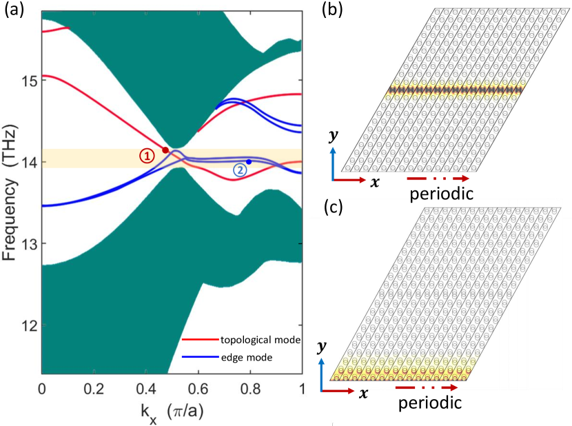
The projected band diagram of a finite bilayer graphene metasurface consisting of 20 unit cells along the -axis and periodic along the -axis is computed, and the results are presented in Fig. 3(a). In this figure, the green regions represent the bulk states and the topological interface modes are marked by red lines. Note that since the bilayer graphene metasurface has a finite number of unit cells along the -axis, there are additional edge modes in Fig. 3(a). More specifically, the blue lines in this figure indicate edge modes confined at the metasurface boundaries rather than the domain-wall interface. In particular, we find that the edge modes generally appear in pairs, at the top and bottom boundaries, and their influence on the domain-wall interface topological modes can be neglected when the number of unit cells of each domain along -axis is larger than about . However, additional functionality can be achieved in a photonic system in which these modes become optically coupled [16, 17].
In order to gain deeper physical insights into the properties of these interface and edge modes, their corresponding field distribution are further investigated. To be more specific, the field distribution of the interface mode ① in Fig. 3(a), given in Fig. 3(b), is highly confined at the domain-wall interface, whereas the field distribution of the edge mode ② in Fig. 3(a), presented in Fig. 3(c), is confined at the boundary of the finite metasurface.
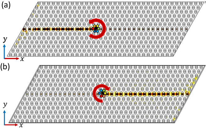
Importantly, we also demonstrated the unidirectional character of light propagation along the domain-wall interface. To illustrate this, we simulated the composite bilayer graphene metasurface with absorbing boundary conditions, but left a certain air space along the -axis to allow for the radiation losses. A monochromatic light source with frequency of was used to excite the proposed composite bilayer graphene metasurface. In order to study the chirality-momentum locking property, which arises from the valley-Hall effects induced by the intrinsic chirality associated to each valley [4], the excitation source was constructed by placing at the corners of a small hexagon six electric dipoles, marked by circles in Fig. 4. In our simulations, the phase difference between neighboring dipoles is set to , so as to implement right-circularly polarized (RCP) and left-circularly polarized (LCP) sources, respectively. More specifically, as illustrated in Fig. 4(a), a RCP light source is placed at the center of the composite bilayer graphene metasurface, and unidirectional propagation of light along the negative direction of the -axis of the domain-wall interface is observed. Similarly, as shown in Fig. 4(b), a LCP light source located at the center of the metasurface, created by reversing the phase difference between adjacent dipoles, excites at the interface a topological mode that propagates along the positive direction of the -axis.
The unidirectional propagation feature of the topological interface mode of the bilayer graphene metasurface investigated in this work can find applications to efficient photonic nanodevices. To illustrate this, in what follows we demonstrate how the interfacial topological mode can be used as the key component of a molecular sensor. Thus, graphene is a particularly promising 2D material for sensing applications, chiefly due to its tunable chemical potential and high optical damage threshold [18]. Generally, the chemical potential of graphene is proportional to the Fermi velocity and the carrier density , which can be tuned via molecular doping, which is a particular type of chemical doping [19]. As such, graphene based sensors can be used to detect the concentration of specific gases in the environment, by measuring the concentration of the corresponding molecules adsorbed onto a graphene sheet. To be more specific, as shown in Fig. 5(a), the proposed bilayer graphene metasurface is used to design a molecular sensor based on the large variations of its optical properties induced by small changes of its chemical characteristics.
The sensor consists of three bilayer graphene metasurfaces, marked as regions I, II, and III, the lengths of these regions being , , and , respectively, and the corresponding chemical potentials . The gas molecules can be adsorbed only in the region II, and upon their adsorption varies. In practice, this can be achieved by covering the regions I and III with some material, e.g., polymethyl methacrylate – PMMA. To add specificity to our analysis, we assume that the gas is NO2. The relation between the variation of the chemical potential induced by NO2 gas with concentration, , is , where the experimentally determined value of is /p.p.m [20, 21, 22]. The variation of the chemical potential in the region II, in turn, leads to a variation of the graphene permittivity, and consequently to a shift of the frequency of the topological band gap associated to region II. This means that, if the frequency of the input light in region I is in the band gap of this region, the corresponding topological interfacial mode can be switched to a leaky bulk mode in the region II. Since the leaky bulk modes are particularly lossy, the output power collected in the region III will sharply decrease.
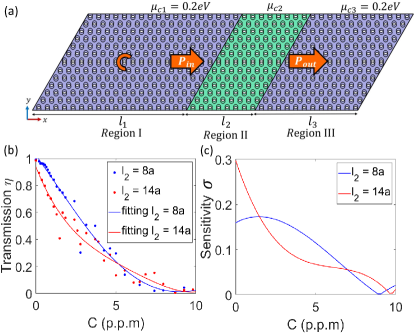
In order to validate these ideas, we have studied the light transmission in the proposed graphene metasurface based molecular sensor. To this end, a monochromatic light source with frequency of is placed in the center of the region I. The lengths of the region I () and region III () are and , respectively. Moreover, we computed the transmission of the optical power, , defined as the ratio between the output power, , collected in the region III and the input power in the region I, namely . These calculations were performed for two different values of the length of region II, namely for and , and the corresponding results are summarized in Fig. 5.
It can be seen in Fig. 5(b), where we plot the dependence of the transmission on the concentration of molecules adsorbed in region II, that the transmission decreases steeply when the concentration of the NO2 gas adsorbed in this region increases. In Fig. 5(b), the dots represent the numerically computed data, whereas the solid lines indicate the fitting of the results via a third-order polynomial. These results prove that, as expected, the longer the length of the region II is, the larger the slope of the transmission curve is, which means that the radiation loss of the input power in the region II is larger. Note also that when p.p.m., the transmission in the case when is larger than when , which is attributable to the constructive interference of the mode propagating in region II, and which undergoes multiple reflections at the interfaces between this region and regions I and III. When the concentration is larger than about p.p.m, most of the input power is scattered out into radiation modes, so that the transmitted power is almost zero in this case. Moreover, we have also studied the sensitivity of the metasurface sensor, , which is defined as the absolute value of the first-order derivative of the transmission with respect to the concentration of NO2 molecules adsorbed in region II, that is, . As shown in Fig. 5(c), the proposed molecular sensor can be used to detect the gas variations in a broad range of molecular concentrations, its sensitivity being particularly large for small concentrations of adsorbed molecules.
In conclusion, we have proposed a novel mechanism to realize valley-Hall topological plasmon transport in a bilayer graphene metasurface. In order to create a topological nontrivial valley bandgap, the lattice of holes of the top layer of the two freestanding graphene layers is horizontally shifted by a certain distance with respect to the bottom layer, such that the mirror symmetry between the top and bottom layers is broken. Moreover, to produce a valley-Hall topological plasmon mode within the nontrivial bandgap, a domain-wall interface is constructed by placing together two bilayer graphene metasurfaces in a way in which the composite metasurface is mirror-symmetric with respect to the interface. The results of our numerical computations show that the proposed domain-wall interfacial waveguide supports topological modes that exhibit unidirectional propagation feature. This property is further used to design a molecular sensor based on the fact that the chemical potential of graphene can by tuned via gas molecule adsorption. Our work could have an important impact on the development of integrated plasmonic devices and key applications pertaining to molecular sensing.
Funding. European Research Council (ERC) (ERC-2014-CoG-648328); China Scholarship Council (CSC); University College London (UCL).
Disclosures. The authors declare no conflicts of interest.
References
- [1] L. Lu, J. D. Joannopoulos, and M. Soljacic, Nat. Photonics 8, 821 (2014).
- [2] A. B. Khanikaev and G. Shvets, Nat. Photonics 11, 763 (2017).
- [3] T. Ozawa, H. M. Price, A. Amo, N. Goldman, M. Hafezi, L. Lu, M. C. Rechtsman, D. Schuster, J. Simon, O. Zilberberg, and I. Carusotto, Rev. Mod. Phys. 91, 015006 (2019).
- [4] D. Xiao, W. Yao, and Q. Niu, Phys. Rev. Lett. 99, 236809 (2007).
- [5] T. Ma and G. Shvets, New J. Phys. 18, 025012 (2016).
- [6] W. Zhang, X. Chen, and F. Ye, Opt. Lett. 42, 4063 (2017).
- [7] J. W. You, Z. Lan, Q. Bao, and N. C. Panoiu, IEEE J. Sel. Top. Quantum Electron. In print, DOI: 10.1109/JSTQE.2020.2982991 (2020).
- [8] D. Jin, T. Christensen, M. Soljacic, N. X. Fang, L. Lu, and X. Zhang, Phys. Rev. Lett. 118, 245301 (2017).
- [9] J. W. You, Z. Lan, and N. C. Panoiu, Sci. Adv. 6, eaaz3910 (2020).
- [10] J. W. You, S. Bongu, Q. Bao, and N. C. Panoiu, Nanophotonics 8, 63 (2018).
- [11] P. A. D. Goncalves and N. M. Peres, An Introduction to Graphene Plasmonics (World Scientific, 2016).
- [12] V. Singh, D. Joung, L. Zhai, S. Das, S. I. Khondaker, and S. Seal, Prog. Mater. Sci. 56, 1178 (2011).
- [13] Y. Zhang, L. Zhang, and C. Zhou, Acc. Chem. Res. 46, 2329 (2013).
- [14] C. Kittel, P. McEuen, and P. McEuen, Introduction to solid state physics, ed. (Wiley New York, 1996).
- [15] B. Y. Xie, H. F. Wang, X. Y. Zhu, M. H. Lu, Z. Wang, and Y. F. Chen, Opt. Express 26, 24531 (2018).
- [16] Y. J. Tsofe and B. A. Malomed, Phys. Rev. E. 75, 056603 (2007).
- [17] S. Ha and A. A. Sukhorukov, J. Opt. Soc. Am. B 25, C15 (2008).
- [18] Q. Bao and K. P. Loh, ACS Nano 6, 3677 (2012).
- [19] D. Rodrigo, O. Limaj, D. Janner, D. Etezadi, F. J. G. De Abajo, V. Pruneri, and H. Altug, Science 349, 165 (2015).
- [20] F. Schedin, A. Geim, S. Morozov, E. Hill, P. Blake, M. Katsnelson, and K. Novoselov, Nat. Mater. 6, 652 (2007).
- [21] H. Hu, X. Yang, X. Guo, K. Khaliji, S. R. Biswas, F. J. G. de Abajo, T. Low, Z. Sun, and Q. Dai, Nat. Commun. 10, 1 (2019).
- [22] K. S. Novoselov, A. K. Geim, S. Morozov, D. Jiang, M. I. Katsnelson, I. Grigorieva, S. Dubonos, and A. A. Firsov, Nature 438, 197 (2005).
- [23] J. N. Anker, W. P. Hall, O. Lyandres, N. C. Shah, J. Zhao, and R. P. Van Duyne, in Nanoscience and Technology: A Collection of Reviews from Nature Journals (World Scientific, 2010) p. 308.