High-yield wafer-scale fabrication of ultralow-loss, dispersion-engineered
silicon nitride photonic circuits
Low-loss photonic integrated circuits (PIC) and microresonators have enabled novel applications ranging from narrow-linewidth lasers Huang et al. (2019a); Xiang et al. (2020), microwave photonics Marpaung et al. (2019); Eggleton et al. (2019), to chip-scale optical frequency combs Kippenberg et al. (2018); Gaeta et al. (2019) and quantum frequency conversion Li et al. (2016); Lu et al. (2019). To translate these results into a widespread technology Agrell et al. (2016), attaining ultralow optical losses with established foundry manufacturing is critical. Recent advances in fabrication of integrated Si3N4 photonics Xuan et al. (2016); Ji et al. (2017); Liu et al. (2018a); Ye et al. (2019); Dirani et al. (2019) have shown that ultralow-loss, dispersion-engineered microresonators can be attained at die-level throughput. For emerging nonlinear applications such as integrated travelling-wave parametric amplifiers Foster et al. (2006); Kuyken et al. (2011); Ooi et al. (2017); Yang et al. (2018) and mode-locked lasers Xin et al. (2019), PICs of length scales of up to a meter are required, placing stringent demands on yield and performance that have not been met with current fabrication techniques. Here we overcome these challenges and demonstrate a fabrication technology which meets all these requirements on wafer-level yield, performance and length scale. Photonic microresonators with a mean factor exceeding , corresponding to a linear propagation loss of 1.0 dB/m, are obtained over full 4-inch wafers, as determined from a statistical analysis of tens of thousands of optical resonances and cavity ringdown with 19 ns photon storage time. The process operates over large areas with high yield, enabling 1-meter-long spiral waveguides with 2.4 dB/m loss in dies of only mm2 size. Using a modulation response measurement self-calibrated via the Kerr nonlinearity, we reveal that, strikingly, the intrinsic absorption-limited factor of our Si3N4 microresonators exceeds . This absorption loss is sufficiently low such that the Kerr nonlinearity dominates the microresonator’s modulation response even in the audio frequency band. Transferring the present Si3N4 photonics technology to standard commercial foundries, and merging it with silicon photonics using heterogeneous integration technology Liang et al. (2010); Park et al. (2020); Blumenthal (2020), will significantly expand the scope of today’s integrated photonics and seed new applications.
Silicon photonics Thomson et al. (2016) has evolved into a mature technology enabling the generation, modulation and detection of optical signals on-chip, via heterogeneous or hybrid integration of different material platforms Liang et al. (2010); Park et al. (2020); Blumenthal (2020). Within the past two decades, it has been transferred from academic research to large-volume commercial deployment in datacenter interconnects. A second revolution is currently under way in which, the optical nonlinearities of PIC - accessed with continuous-wave lasers at sub-milliwatt power - become relevant for applications, i.e. integrated nonlinear photonics. The Kerr, or Brillouin nonlinearities enable novel schemes for nonlinear optical signal generation and processing Marpaung et al. (2019); Gaeta et al. (2019); Wang et al. (2018). Major effort has been made in the past decade in developing various integrated nonlinear photonic platforms ranging from Si3N4 Xuan et al. (2016); Ji et al. (2017); Liu et al. (2018a); Ye et al. (2019); Dirani et al. (2019), diamond Hausmann et al. (2014), Ta2O5 Jung et al. (2019), SiC Lukin et al. (2020) to highly nonlinear AlGaAs Pu et al. (2016); Chang et al. (2020) and GaP Wilson et al. (2020) on insulator, as well as electro-optic platforms such as LiNbO3 Wang et al. (2018); Zhang et al. (2019); He et al. (2019); Fang et al. (2019) and AlN Jung et al. (2014); Guo et al. (2016); Liu et al. (2018b, c). Significant progress has been achieved on harnessing the Kerr nonlinearity which enables the generation of dissipative Kerr soliton microcombs in integrated optical microresonators Kippenberg et al. (2018); Gaeta et al. (2019). Microcombs constitute chip-scale frequency combs with broad bandwidths and repetition rates in the microwave domain, amenable to heterogeneous or hybrid integration with III-V/Si lasers Stern et al. (2018); Raja et al. (2019), and have been used in system-level demonstrations including coherent telecommunications Marin-Palomo et al. (2017), integrated frequency synthesizers Spencer et al. (2018), astronomical spectrometer calibration Obrzud et al. (2019); Suh et al. (2019), ultrafast ranging Trocha et al. (2018); Suh and Vahala (2018), low-noise microwave generation Liang et al. (2015); Liu et al. (2020) and massively parallel coherent LiDAR Riemensberger et al. (2020).
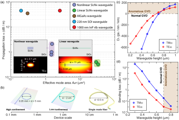
For nonlinear integrated photonics, Si3N4 Levy et al. (2010); Moss et al. (2013); Blumenthal et al. (2018) has emerged as a leading material due to its ultralow linear and nonlinear optical losses, strong Kerr nonlinearity, high refractive index, and high power handling capability Gyger et al. (2020). To date, among all integrated photonics platforms Kovach et al. (2020), optical losses near or below 1 dB/m have only been demonstrated in Si3N4 waveguides. First achieved in thin-core waveguides (e.g. waveguide height nm) Spencer et al. (2014); Gundavarapu et al. (2019); Bauters et al. (2011), ultralow losses have later also been attained in thick-core (i.e. nm) Xuan et al. (2016); Ji et al. (2017); Liu et al. (2018a) waveguides enabling negligible bending loss, dispersion engineering and significantly higher Kerr nonlinearity, as outlined in Fig. 1. Many system-level demonstrations of soliton microcombs Marin-Palomo et al. (2017); Obrzud et al. (2019); Trocha et al. (2018); Liu et al. (2020); Riemensberger et al. (2020) have been based on this type of Si3N4 PICs. Figure 1(a) highlights the lowest-loss nonlinear (ref. Xuan et al. (2016); Ji et al. (2017) and this work) and linear Spencer et al. (2014); Gundavarapu et al. (2019) Si3N4 waveguides in terms of their optical losses and effective area of the fundamental optical mode, in comparison with the state-of-the-art, lowest-loss silicon Selvaraja et al. (2014), InP Ciminelli et al. (2013) and AlGaAs Chang et al. (2020) waveguides. The tight confinement significantly relaxes the bending loss, a key parameter for device footprint and photonic integration, as outlined in Fig. 1(b). Though the desirable combination of tight confinement, ultralow loss and anomalous GVD has been achieved to date Xuan et al. (2016); Ji et al. (2017), it has only been attained in individual chips, i.e. with die-level throughput. Meanwhile, the fabrication of densely packed, meter-long PIC has not been achieved. Nor has wafer-level fabrication yield, reliability and reproducibility, required for widespread adoption in CMOS foundries, been demonstrated. Yet, densely packed, meter-long nonlinear Si3N4 PIC could enable a new class of devices, ranging from integrated travelling-wave parametric amplifiers Foster et al. (2006); Kuyken et al. (2011); Ooi et al. (2017); Yang et al. (2018) to integrated mode-locked-lasers based on rare-earth doping Xin et al. (2019).

Here we report a high-yield wafer-scale fabrication technology to build tight-confinement, ultralow-loss, dispersion-engineered Si3N4 waveguides of length scales up to more than a meter. It is based on the photonic Damascene process Pfeiffer et al. (2018a) using standard CMOS fabrication techniques such as DUV stepper lithography, dry etching and low-pressure chemical vapor deposition (LPCVD). Figure 2(a) shows process flow and scanning electron micrographs (SEM) for selected key steps. The waveguides and stress-release filler patterns Pfeiffer et al. (2018a) are written directly on the SiO2 substrate via DUV stepper lithography based on 248 nm KrF excimer laser. The use of DUV, in contrast to the commonly employed electron-beam lithography, enables dramatic increase in throughput, stability and reproducibility, essential to large-volume manufacturing. The patterns are then dry-etched to the SiO2 substrate to create waveguide preforms. We note that our SiO2 dry etching does not introduce a trade-off between the etch verticality and surface roughness. Figure 2(d) top shows the sidewall bottom angle . To further reduce the waveguide sidewall roughness (root mean square) to sub-nanometer level, the entire substrate is annealed at 1250∘C (“preform reflow”) Pfeiffer et al. (2018b). Importantly, this reflow process can further reduce the scattering loss, and does not lead to prominent deformation of the waveguide preform. Figure 2(d) bottom shows the measured sidewall bottom angle . An LPCVD Si3N4 film of 1000 nm thickness is deposited on the patterned substrate, filling the preform trenches and forming the waveguides. A novel etchback planarization process is applied, combining photoresist coating, dry etching and chemical-mechanical planarization (CMP). This process enables full control of polishing depth and wafer-scale uniformity with variation below 3%. Afterwards, the entire substrate is thermally annealed at 1200∘C to drive out the residual hydrogen impurities in the Si3N4 film Liu et al. (2018a). Top SiO2 cladding composed of TEOS and low-temperature oxide (LTO) are deposited on the wafer, followed by SiO2 thermal annealing. Finally, the wafer is separated into chips via deep dry etching followed by dicing or backside grinding, to attain chip facets with superior quality which is critical for edge coupling Raja et al. (2019); Shen et al. ; Voloshin et al. .
Figure 2(b) shows the final Si3N4 chips containing multiple ring resonators of different free spectral ranges (FSR). Figure 2(c) shows the optical micrograph of the Si3N4 ring resonator, bus waveguide and filler patterns, as well as the tightly confined waveguide mode. The resulted negligible bending loss allows microresonators of small radii below 23 m (i.e. 1 THz FSR), which find wide applications in optical filters and coupled-resonator-based delay lines Poon et al. (2004); Cardenas et al. (2010). The filler patterns consist of horizontal and vertical bars uniformly distributed over the entire wafer area, and can significantly relax the as-deposited LPCVD Si3N4 film stress for crack prevention. These filler patterns are also required for etching and CMP uniformity.
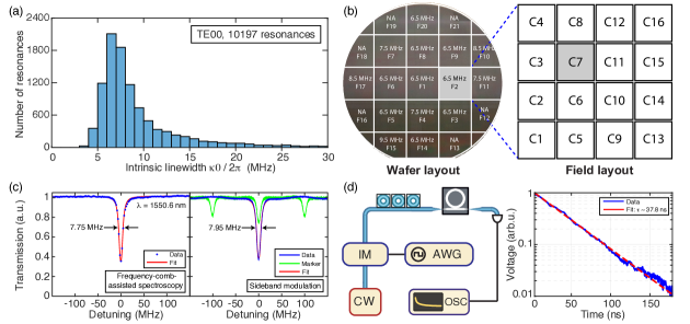
Statistical analysis of microresonator factors: We fabricate Si3N4 microresonators of 40.6 GHz FSR, 2200 nm width and 950 nm height, and systematically study the microresonator factors (i.e. loss). Frequency-comb-assisted diode laser spectroscopy Del’Haye et al. (2009); Liu et al. (2016) is used to characterize the resonance frequency and linewidth , which relate to the resonance factor as . Here we mainly study the fundamental transverse electric (TE00) mode. The total (loaded) linewidth , the intrinsic loss and the coupling strength are extracted from each resonance fit. Figure 3(a) shows the histogram of 10,197 TE00 resonances measured from twenty-six microresonators. The most probable value is MHz, corresponding to an intrinsic factor of . In comparison, MHz is found for the fundamental transverse magnetic (TM00) mode, corresponding to . Finally, as the threshold power for soliton formation scales as , such high microresonator allows soliton formation of 40 GHz repetition rate with only 10 mW optical power, without using an optical power amplifier (The measured GVD is kHz).
Next, we demonstrate wafer-scale yield of our fabrication technology. Figure 3(b) shows our mask layout comprising chip designs on the DUV stepper reticle. Each chip has a mm2 size, and contains multiple microresonators as shown in Fig. 2(b). The DUV stepper writes the reticle pattern uniformly over the full 4-inch wafer in discrete fields. The calibration chips of 40 GHz FSR studied here are the C7 chips. The most probable value of histograms of C7 chips is measured and plotted in each exposure field, as shown in Fig. 3(b). In most fields, MHz is found. While exceptionally narrow linewidth has been reported previously on individual resonances, our statistics based on tens of thousands of analyzed resonances from dozens of samples at different wafer positions, shows wafer-scale fabrication throughput and yield.
In addition, sideband modulation technique Li et al. (2012) is performed to measure the resonance linewidth and to fit . Two sidebands, each separated from the carrier by 100 MHz, are used to calibrate the resonance linewidth. Figure 3(c) compares the measured and fitted of the same resonance which does not present a visible mode split, using both the frequency-comb-assisted diode laser spectroscopy ( MHz and MHz) and the sideband modulation technique ( MHz and MHz). Both methods agree with each other, and show .
Furthermore, cavity ring-down measurement is performed to validate the measured linewidth (see Method). Figure 3(d) shows the schematic of the experimental setup and a representative ring-down measurement data. The fitted optical field decay time is 37.8 ns, corresponding to 18.9 ns photon storage time. The calculated loaded linewidth is MHz, showing consistency between the three characterization methods used here.
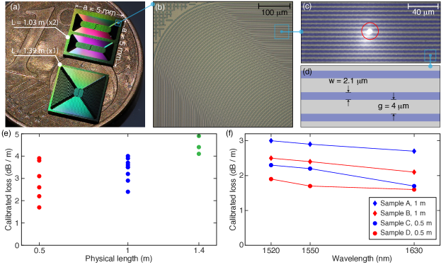
Meter-long spiral waveguides: In addition to high- microresonators, we also fabricate and characterize meter-long spiral waveguides that are key elements to build photonic true-time delay lines. Previously, silica suspended wedge waveguides Lee et al. (2012) and thin-core Si3N4 waveguides Bauters et al. (2011) have been studied to build delay lines with losses below 0.1 dB/m. However, as a result of avoiding bending losses, these waveguides occupy more than 20 cm2 areas, thus suffering from significant device footprints. While tight optical confinement can reduce the footprint, losses approaching even 1 dB/m have not been achieved in any nonlinear waveguide including thick-core Si3N4. Here, we demonstrate meter-long Si3N4 waveguides featuring ultralow loss and small footprint, which can enable key applications for travelling-wave parametric amplifiers Foster et al. (2006); Kuyken et al. (2011); Ooi et al. (2017); Yang et al. (2018), rare-earth-doped mode-locked lasers Xin et al. (2019) and optical coherence tomography (OCT) Ji et al. (2019).
Figure 4(a) shows a photograph of photonic chips containing Si3N4 waveguides of physical lengths longer than 1 m. Figure 4(b, c, d) shows the spiral layout. The waveguides are densely packed in Archimedean spirals, with waveguide width m and gap distance m. Three lengths are studied here: a 0.5-meter-long spiral contains 50 coils and covers 3.1 mm2 area; a 1.0-meter-long spiral contains 106 coils and covers 6.6 mm2 area; and a 1.4-meter-long spiral contains 130 coils and covers 20.2 mm2 area. Compared with the previous report based on thin-core Si3N4 waveguides Bauters et al. (2011) showing a device footprint of more than 20 cm2 area for 1 m physical length, our devices represent a footprint reduction of 300 times, critical for photonic integration. Figure 4(e) shows the measured losses in multiples samples, calibrated using the adjacent 5-millimeter-long waveguide which has a fiber-chip-fiber through coupling efficiency of 33% (4.8 dB for two chip facets). The lowest loss values found are 1.7 dB/m for 0.5 m length, 2.4 dB/m for 1.0 m length, and 4.1 dB/m for 1.4 m length. These loss values are higher than the value extrapolated from microresonator characterization (1.0 dB/m). Meanwhile, the overall trend shows higher losses in longer waveguides. We attribute both observations to the extra light-scattering defects. Light-scattering defects are found under an infrared (IR) microscope, as shown in Fig. 4(c). By counting the number of defects in high-loss spirals, we estimate that each defect causes 1–2 dB extra loss. The probability of defects depends on the waveguide area. These defects are likely caused by particle contamination on the wafer, as we have verified that these defects are not on the DUV reticle which would generate the same defects in the same position in each exposure field. Figure 4(f) shows the calibrated losses measured at different wavelengths for four selected samples. A trend showing a higher loss at a shorter wavelength is observed.
Quantitative analysis of loss limit: Next, we investigate quantitatively the intrinsic absorption and scattering losses of our Si3N4 waveguides. The optical losses in the telecommunication band have two main contributions: the Rayleigh scattering loss caused mainly by the waveguide sidewall roughness, and the absorption loss due to e.g. hydrogen impurities. While the hydrogen absorption loss can be efficiently eliminated via repeated thermal annealing of Si3N4 at high temperature C Luke et al. (2015); Liu et al. (2018a), efforts on loss reduction have mainly focused on reducing waveguide roughness via optimized dry etching Ji et al. (2017), wet etching Huang et al. (2015), and etchless process Griffith et al. (2012); Kim et al. (2019). In addition, the large mode area of thin-core Si3N4 waveguides Bauters et al. (2011); Gundavarapu et al. (2019); Spencer et al. (2014) results in reduced optical mode interaction with waveguide sidewall roughness, and thereby reduced scattering losses.
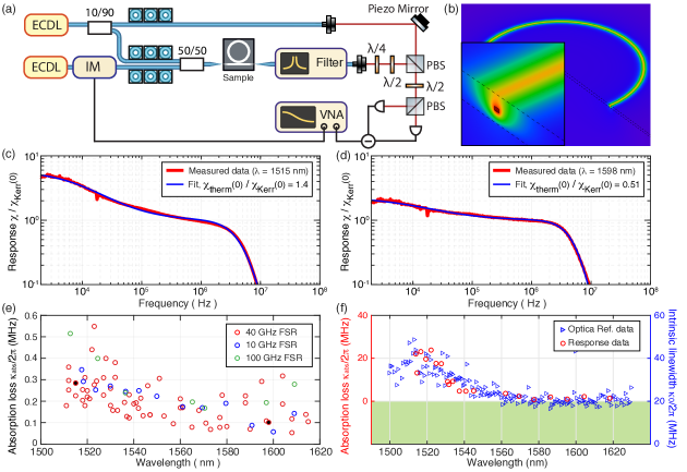
To quantify the thermal absorption loss of our Si3N4 waveguides, a modulation response measurement Wilson et al. (2020) is performed. The experimental setup is shown in Fig. 5(a), with two lasers, the pump and probe. The pump laser is tuned to an optical resonance whose frequency is , and the thermal absorption loss in this resonance is to be characterized. Meanwhile, the pump laser is intensity-modulated with frequency . The probe laser is loosely locked (i.e. low-bandwidth locking) to another optical resonance whose frequency is . The principle of the linear microresonator response measurement is to characterize the resonance frequency shift of the probe mode induced by the intensity modulation of the pump mode . This intensity modulation causes intracavity power modulation (i.e. photon number modulation ), which modulates the resonance frequency of the probe mode via Kerr and thermal nonlinearities. The pump power is maintained sufficiently low, such that the steady-state frequency shift of the probe mode is small compared to the resonance linewidth , i.e. . In this linear regime, the frequency response to the modulating pump power is given by Wilson et al. (2020)
| (1) |
The total response consists of two parts: the Kerr response with infinite bandwidth, and the thermal response with a bandwidth below 20 kHz. Therefore, by calibrating the response as a function of the modulation frequency , and can be individually identified. Using the values of and at DC (), the absorption rate is calculated as
| (2) |
where is the effective optical mode volume, mW is the nonlinear index of Si3N4, is the group index, is the material index and K is the thermo-optic coefficient Arbabi and Goddard (2013), and is the absorbed power.
The frequency response to the pump modulation is transduced into the probe laser’s phase modulation. The phase response is measured using a balanced homodyne detection, with the pump laser being filtered out before detection (see Methods). To evaluate the absorption rate , the factor is retrieved by a two-pole fitting of the measured response , which presents a thermal cutoff frequency and a cavity cutoff frequency . The fitting exploits the fact that the thermal response dominates at frequency below 10 kHz and has a cutoff frequency kHz. At higher frequency, the Kerr response dominates. Figure 5(c, d) present two examples of measured and fitted . Finite-element simulations of optical mode profiles and bulk absorption heating are performed to calculate the coefficients and . Figure 5(b) shows the temperature profile from the thermal simulation (see Method).
Figure 5(e) shows the calculated absorption rates of different resonances from four 40-GHz-FSR Si3N4 samples featuring , in comparison with 10- and 100-GHz-FSR samples fabricated using the same process but from different wafers. All samples show similar trends, and present two conclusions. First, the mean absorption loss is only MHz, corresponding an absorption-loss-limited factor of . Therefore, the optical losses of our Si3N4 waveguides ( MHz) are currently dominated by scattering losses. Second, is higher ( MHz) around 1520 nm, compared to the value at e.g. 1600 nm ( MHz). This is caused by the residual hydrogen impurities in our thermally annealed Si3N4. Note that, only standard LPCVD Si3N4 / SiO2 films and thermal annealing are used in our fabrication to achieve such low absorption losses.
To validate our findings, we further benchmark the linear response measurement by characterizing a partially annealed Si3N4 sample whose resonance linewidth data have been published in ref. Liu et al. (2018a). We characterize again this particular sample, using both the response measurement and the frequency-comb-assisted diode laser spectroscopy, and compare the results using both methods in Fig. 5(f). Assuming a wavelength-independent scattering loss of 20 MHz, the measured hydrogen absorption loss using the response measurement agrees with the total loss measured using the other method.
Conclusion: We have demonstrated a fabrication technology enabling high-yield and reproducible wafer-scale manufacturing of ultralow-loss, high-confinement, anomalous-GVD Si3N4 PIC. We present a statistical study of microresonator losses based on tens of thousands of analyzed resonances. We further reveal that our waveguide losses are dominated by scattering losses, which could be further reduced via e.g. optimized lithography and etching. In the ideal case limited only by the thermal absorption loss, the potential microresonator is calculated to exceed (corresponding to a linear loss of 0.03 dB/m). The optimized photonic Damascene fabrication technology allows tight-confinement, ultralow-loss, high-yield, meter-scale, nonlinear PIC, and is suitable for adoption in CMOS foundries.
Methods
Cavity ringdown: An intensity modulator (IM) is used to rapidly switch on and off the pump field. The ring-down signal of the transmitted light is recorded by a 1-GHz-bandwidth low-noise photodetector. A 50-kHz square wave electrical drive signal is generated using a fast arbitrary waveform generator, ensuring that the light is switched off significantly faster than the resonance linewidth. The upper and lower voltage levels of the square wave are adjusted to match the maximum and minimum transmission voltage of the IM, such that the electrical overshoot and undershoot of the square wave signal do not twist the ring-down slope. Due to the finite extinction ratio of the IM, the residual pump field beats with the leakage of the intracavity field, producing a field ring-down signal which is affected by the detuning of the laser from the cavity mode resonances Wójtewicz et al. (2018). At small detunings (), the effective ring-down rate is increased by the laser’s detuning from cavity resonance, and thus the directly inferred quality factor is less accurate than the sideband fitting result. Therefore, the ring-down results can only serve as a lower bound of the loaded factor of the measured resonances. The estimated loaded linewidth MHz is in agreement with the sideband fitting results, showing consistency between the three characterization methods used here.
Thermal simulations: We use COMSOL Multiphysics to simulate the thermal response due to bulk absorption heating of our Si3N4 samples. The main material property coefficients of interest used in the current simulation are identical to the ones used in ref.Huang et al. (2019b) for simulating the Si3N4 thermal refractive noise. We first simulate the waveguide optical mode profile (TE00 mode), from which the effective mode volume is calculated. Bulk absorption heating is introduced whose power distribution is proportional to the intensity distribution of the optical mode . From the stationary study of the sample heating, the dependence of temperature change on absorbed power, , is retrieved from an absorption power sweep. The combined value of is calculated as in the case of full SiO2 cladding for samples used in Fig. 5(c, d, e), and is in the case of missing top SiO2 cladding for samples used in Fig. 5(f).
Response calibration: In order to extract the actual microresonator response from the experimentally photodetected , the frequency response of our entire experiment setup and detection chain needs to be calibrated first. This is realized by direct detection of the pump power modulation in the absence of the probe laser and the pump filter. The measured response is normalized to the setup response , and thus the actual microresonator response is retrieved, with an uncertain constant factor. This constant factor is removed when retrieving from the two pole fitting of using a fitting function
with and being the thermal and cavity cutoff frequencies, being the parameter accounting for the material inhomogeneity (that is, the Si3N4 waveguide has a finite dimension and is surrounded by SiO2 cladding). In Fig. 5(c, d), only the normalized response is shown, with the uncertain constant factor removed.
Funding Information: This work was supported by Contract HR0011-15-C-055 (DODOS) from the Defense Advanced Research Projects Agency (DARPA), Microsystems Technology Office (MTO), by the Air Force Office of Scientific Research, Air Force Materiel Command, USAF under Award No. FA9550-15-1-0250, and by Swiss National Science Foundation under grant agreement No. 176563. (BRIDGE).
Acknowledgments: We thank Bahareh Ghadiani for the assistance in the fabrication process development in the early stage, and Qi-Fan Yang for the fruitful discussion. The Si3N4 microresonator samples were fabricated in the EPFL center of MicroNanoTechnology (CMi).
Data Availability Statement: The code and data used to produce the plots within this work will be released on the repository Zenodo upon publication of this preprint.
References
- Huang et al. (2019a) D. Huang, M. A. Tran, J. Guo, J. Peters, T. Komljenovic, A. Malik, P. A. Morton, and J. E. Bowers, Optica 6, 745 (2019a).
- Xiang et al. (2020) C. Xiang, W. Jin, J. Guo, J. D. Peters, M. J. Kennedy, J. Selvidge, P. A. Morton, and J. E. Bowers, Optica 7, 20 (2020).
- Marpaung et al. (2019) D. Marpaung, J. Yao, and J. Capmany, Nature Photonics 13, 80 (2019).
- Eggleton et al. (2019) B. J. Eggleton, C. G. Poulton, P. T. Rakich, M. J. Steel, and G. Bahl, Nature Photonics 13, 664 (2019).
- Kippenberg et al. (2018) T. J. Kippenberg, A. L. Gaeta, M. Lipson, and M. L. Gorodetsky, Science 361 (2018), 10.1126/science.aan8083.
- Gaeta et al. (2019) A. L. Gaeta, M. Lipson, and T. J. Kippenberg, Nature Photonics 13, 158 (2019).
- Li et al. (2016) Q. Li, M. Davanço, and K. Srinivasan, Nature Photonics 10, 406 EP (2016).
- Lu et al. (2019) X. Lu, G. Moille, Q. Li, D. A. Westly, A. Singh, A. Rao, S.-P. Yu, T. C. Briles, S. B. Papp, and K. Srinivasan, Nature Photonics 13, 593 (2019).
- Agrell et al. (2016) E. Agrell, M. Karlsson, A. R. Chraplyvy, D. J. Richardson, P. M. Krummrich, P. Winzer, K. Roberts, J. K. Fischer, S. J. Savory, B. J. Eggleton, M. Secondini, F. R. Kschischang, A. Lord, J. Prat, I. Tomkos, J. E. Bowers, S. Srinivasan, M. Brandt-Pearce, and N. Gisin, Journal of Optics 18, 063002 (2016).
- Xuan et al. (2016) Y. Xuan, Y. Liu, L. T. Varghese, A. J. Metcalf, X. Xue, P.-H. Wang, K. Han, J. A. Jaramillo-Villegas, A. A. Noman, C. Wang, S. Kim, M. Teng, Y. J. Lee, B. Niu, L. Fan, J. Wang, D. E. Leaird, A. M. Weiner, and M. Qi, Optica 3, 1171 (2016).
- Ji et al. (2017) X. Ji, F. A. S. Barbosa, S. P. Roberts, A. Dutt, J. Cardenas, Y. Okawachi, A. Bryant, A. L. Gaeta, and M. Lipson, Optica 4, 619 (2017).
- Liu et al. (2018a) J. Liu, A. S. Raja, M. Karpov, B. Ghadiani, M. H. P. Pfeiffer, B. Du, N. J. Engelsen, H. Guo, M. Zervas, and T. J. Kippenberg, Optica 5, 1347 (2018a).
- Ye et al. (2019) Z. Ye, A. Fülöp, Óskar Bjarki Helgason, P. A. Andrekson, and V. Torres-Company, Opt. Lett. 44, 3326 (2019).
- Dirani et al. (2019) H. E. Dirani, L. Youssef, C. Petit-Etienne, S. Kerdiles, P. Grosse, C. Monat, E. Pargon, and C. Sciancalepore, Opt. Express 27, 30726 (2019).
- Foster et al. (2006) M. A. Foster, A. C. Turner, J. E. Sharping, B. S. Schmidt, M. Lipson, and A. L. Gaeta, Nature 441, 960 (2006).
- Kuyken et al. (2011) B. Kuyken, X. Liu, G. Roelkens, R. Baets, J. Richard M. Osgood, and W. M. J. Green, Opt. Lett. 36, 4401 (2011).
- Ooi et al. (2017) K. J. A. Ooi, D. K. T. Ng, T. Wang, A. K. L. Chee, S. K. Ng, Q. Wang, L. K. Ang, A. M. Agarwal, L. C. Kimerling, and D. T. H. Tan, Nature Communications 8, 13878 (2017).
- Yang et al. (2018) M. Yang, L. Xu, J. Wang, H. Liu, X. Zhou, G. Li, and L. Zhang, IEEE Journal of Selected Topics in Quantum Electronics, IEEE Journal of Selected Topics in Quantum Electronics 24, 1 (2018).
- Xin et al. (2019) M. Xin, N. Li, N. Singh, A. Ruocco, Z. Su, E. S. Magden, J. Notaros, D. Vermeulen, E. P. Ippen, M. R. Watts, and F. X. Kärtner, Light: Science & Applications 8, 122 (2019).
- Liang et al. (2010) D. Liang, G. Roelkens, R. Baets, and J. E. Bowers, Materials 3, 1782 (2010).
- Park et al. (2020) H. Park, C. Zhang, M. A. Tran, and T. Komljenovic, Optica 7, 336 (2020).
- Blumenthal (2020) D. J. Blumenthal, APL Photonics 5, 020903 (2020).
- Thomson et al. (2016) D. Thomson, A. Zilkie, J. E. Bowers, T. Komljenovic, G. T. Reed, L. Vivien, D. Marris-Morini, E. Cassan, L. Virot, J.-M. Fédéli, J.-M. Hartmann, J. H. Schmid, D.-X. Xu, F. Boeuf, P. O’Brien, G. Z. Mashanovich, and M. Nedeljkovic, Journal of Optics 18, 073003 (2016).
- Wang et al. (2018) C. Wang, M. Zhang, X. Chen, M. Bertrand, A. Shams-Ansari, S. Chandrasekhar, P. Winzer, and M. Lončar, Nature 562, 101 (2018).
- Hausmann et al. (2014) B. J. M. Hausmann, I. Bulu, V. Venkataraman, P. Deotare, and M. Lončar, Nature Photonics 8, 369 EP (2014).
- Jung et al. (2019) H. Jung, S.-P. Yu, D. R. Carlson, T. E. Drake, T. C. Briles, and S. B. Papp, in Nonlinear Optics (NLO) (Optical Society of America, 2019) p. NW2A.3.
- Lukin et al. (2020) D. M. Lukin, C. Dory, M. A. Guidry, K. Y. Yang, S. D. Mishra, R. Trivedi, M. Radulaski, S. Sun, D. Vercruysse, G. H. Ahn, and J. Vučković, Nature Photonics 14, 330 (2020).
- Pu et al. (2016) M. Pu, L. Ottaviano, E. Semenova, and K. Yvind, Optica 3, 823 (2016).
- Chang et al. (2020) L. Chang, W. Xie, H. Shu, Q.-F. Yang, B. Shen, A. Boes, J. D. Peters, W. Jin, C. Xiang, S. Liu, G. Moille, S.-P. Yu, X. Wang, K. Srinivasan, S. B. Papp, K. Vahala, and J. E. Bowers, Nature Communications 11, 1331 (2020).
- Wilson et al. (2020) D. J. Wilson, K. Schneider, S. Hönl, M. Anderson, Y. Baumgartner, L. Czornomaz, T. J. Kippenberg, and P. Seidler, Nature Photonics 14, 57 (2020).
- Zhang et al. (2019) M. Zhang, B. Buscaino, C. Wang, A. Shams-Ansari, C. Reimer, R. Zhu, J. M. Kahn, and M. Lončar, Nature 568, 373 (2019).
- He et al. (2019) Y. He, Q.-F. Yang, J. Ling, R. Luo, H. Liang, M. Li, B. Shen, H. Wang, K. Vahala, and Q. Lin, Optica 6, 1138 (2019).
- Fang et al. (2019) Z. Fang, H. Luo, J. Lin, M. Wang, J. Zhang, R. Wu, J. Zhou, W. Chu, T. Lu, and Y. Cheng, Opt. Lett. 44 (2019), 10.1364/OL.44.005953.
- Jung et al. (2014) H. Jung, K. Y. Fong, C. Xiong, and H. X. Tang, Opt. Lett. 39, 84 (2014).
- Guo et al. (2016) X. Guo, C.-L. Zou, and H. X. Tang, Optica 3, 1126 (2016).
- Liu et al. (2018b) X. Liu, C. Sun, B. Xiong, L. Wang, J. Wang, Y. Han, Z. Hao, H. Li, Y. Luo, J. Yan, T. Wei, Y. Zhang, and J. Wang, ACS Photonics, ACS Photonics 5, 1943 (2018b).
- Liu et al. (2018c) X. Liu, C. Sun, B. Xiong, L. Wang, J. Wang, Y. Han, Z. Hao, H. Li, Y. Luo, J. Yan, T. Wei, Y. Zhang, and J. Wang, Applied Physics Letters 113, 171106 (2018c).
- Stern et al. (2018) B. Stern, X. Ji, Y. Okawachi, A. L. Gaeta, and M. Lipson, Nature 562, 401 (2018).
- Raja et al. (2019) A. S. Raja, A. S. Voloshin, H. Guo, S. E. Agafonova, J. Liu, A. S. Gorodnitskiy, M. Karpov, N. G. Pavlov, E. Lucas, R. R. Galiev, A. E. Shitikov, J. D. Jost, M. L. Gorodetsky, and T. J. Kippenberg, Nature Communications 10, 680 (2019).
- Marin-Palomo et al. (2017) P. Marin-Palomo, J. N. Kemal, M. Karpov, A. Kordts, J. Pfeifle, M. H. P. Pfeiffer, P. Trocha, S. Wolf, V. Brasch, M. H. Anderson, R. Rosenberger, K. Vijayan, W. Freude, T. J. Kippenberg, and C. Koos, Nature 546, 274 (2017).
- Spencer et al. (2018) D. T. Spencer, T. Drake, T. C. Briles, J. Stone, L. C. Sinclair, C. Fredrick, Q. Li, D. Westly, B. R. Ilic, A. Bluestone, N. Volet, T. Komljenovic, L. Chang, S. H. Lee, D. Y. Oh, M.-G. Suh, K. Y. Yang, M. H. P. Pfeiffer, T. J. Kippenberg, E. Norberg, L. Theogarajan, K. Vahala, N. R. Newbury, K. Srinivasan, J. E. Bowers, S. A. Diddams, and S. B. Papp, Nature 557, 81 (2018).
- Obrzud et al. (2019) E. Obrzud, M. Rainer, A. Harutyunyan, M. H. Anderson, J. Liu, M. Geiselmann, B. Chazelas, S. Kundermann, S. Lecomte, M. Cecconi, A. Ghedina, E. Molinari, F. Pepe, F. Wildi, F. Bouchy, T. J. Kippenberg, and T. Herr, Nature Photonics 13, 31 (2019).
- Suh et al. (2019) M.-G. Suh, X. Yi, Y.-H. Lai, S. Leifer, I. S. Grudinin, G. Vasisht, E. C. Martin, M. P. Fitzgerald, G. Doppmann, J. Wang, D. Mawet, S. B. Papp, S. A. Diddams, C. Beichman, and K. Vahala, Nature Photonics 13, 25 (2019).
- Trocha et al. (2018) P. Trocha, M. Karpov, D. Ganin, M. H. P. Pfeiffer, A. Kordts, S. Wolf, J. Krockenberger, P. Marin-Palomo, C. Weimann, S. Randel, W. Freude, T. J. Kippenberg, and C. Koos, Science 359, 887 (2018).
- Suh and Vahala (2018) M.-G. Suh and K. J. Vahala, Science 359, 884 (2018).
- Liang et al. (2015) W. Liang, D. Eliyahu, V. S. Ilchenko, A. A. Savchenkov, A. B. Matsko, D. Seidel, and L. Maleki, Nature Communications 6, 7957 (2015).
- Liu et al. (2020) J. Liu, E. Lucas, A. S. Raja, J. He, J. Riemensberger, R. N. Wang, M. Karpov, H. Guo, R. Bouchand, and T. J. Kippenberg, Nature Photonics (2020), 10.1038/s41566-020-0617-x.
- Riemensberger et al. (2020) J. Riemensberger, A. Lukashchuk, M. Karpov, W. Weng, E. Lucas, J. Liu, and T. J. Kippenberg, Nature 581, 164 (2020).
- Spencer et al. (2014) D. T. Spencer, J. F. Bauters, M. J. R. Heck, and J. E. Bowers, Optica 1, 153 (2014).
- Gundavarapu et al. (2019) S. Gundavarapu, G. M. Brodnik, M. Puckett, T. Huffman, D. Bose, R. Behunin, J. Wu, T. Qiu, C. Pinho, N. Chauhan, J. Nohava, P. T. Rakich, K. D. Nelson, M. Salit, and D. J. Blumenthal, Nature Photonics 13, 60 (2019).
- Selvaraja et al. (2014) S. K. Selvaraja, P. D. Heyn, G. Winroth, P. Ong, G. Lepage, C. Cailler, A. Rigny, K. K. Bourdelle, W. Bogaerts, D. V. Thourhout, J. V. Campenhout, and P. Absil, in Optical Fiber Communication Conference (Optical Society of America, 2014) p. Th2A.33.
- Ciminelli et al. (2013) C. Ciminelli, F. Dell’Olio, M. N. Armenise, F. M. Soares, and W. Passenberg, Opt. Express 21, 556 (2013).
- Levy et al. (2010) J. S. Levy, A. Gondarenko, M. A. Foster, A. C. Turner-Foster, A. L. Gaeta, and M. Lipson, Nature Photonics 4, 37 (2010).
- Moss et al. (2013) D. J. Moss, R. Morandotti, A. L. Gaeta, and M. Lipson, Nature Photonics 7, 597 (2013).
- Blumenthal et al. (2018) D. J. Blumenthal, R. Heideman, D. Geuzebroek, A. Leinse, and C. Roeloffzen, Proceedings of the IEEE 106, 2209 (2018).
- Gyger et al. (2020) F. Gyger, J. Liu, F. Yang, J. He, A. S. Raja, R. N. Wang, S. A. Bhave, T. J. Kippenberg, and L. Thévenaz, Phys. Rev. Lett. 124, 013902 (2020).
- Kovach et al. (2020) A. Kovach, D. Chen, J. He, H. Choi, A. H. Dogan, M. Ghasemkhani, H. Taheri, and A. M. Armani, Adv. Opt. Photon. 12, 135 (2020).
- Bauters et al. (2011) J. F. Bauters, M. J. R. Heck, D. D. John, J. S. Barton, C. M. Bruinink, A. Leinse, R. G. Heideman, D. J. Blumenthal, and J. E. Bowers, Opt. Express 19, 24090 (2011).
- Pfeiffer et al. (2018a) M. H. P. Pfeiffer, C. Herkommer, J. Liu, T. Morais, M. Zervas, M. Geiselmann, and T. J. Kippenberg, IEEE Journal of Selected Topics in Quantum Electronics 24, 1 (2018a).
- Pfeiffer et al. (2018b) M. H. P. Pfeiffer, J. Liu, A. S. Raja, T. Morais, B. Ghadiani, and T. J. Kippenberg, Optica 5, 884 (2018b).
- (61) B. Shen, L. Chang, J. Liu, H. Wang, Q.-F. Yang, C. Xiang, R. N. Wang, J. He, T. Liu, W. Xie, J. Guo, D. Kinghorn, L. Wu, Q.-X. Ji, T. J. Kippenberg, K. Vahala, and J. E. Bowers, arXiv 1911.02636.
- (62) A. S. Voloshin, J. Liu, N. M. Kondratiev, G. V. Lihachev, T. J. Kippenberg, and I. A. Bilenko, arXiv 1912.11303.
- Poon et al. (2004) J. K. S. Poon, J. Scheuer, Y. Xu, and A. Yariv, J. Opt. Soc. Am. B 21, 1665 (2004).
- Cardenas et al. (2010) J. Cardenas, M. A. Foster, N. Sherwood-Droz, C. B. Poitras, H. L. R. Lira, B. Zhang, A. L. Gaeta, J. B. Khurgin, P. Morton, and M. Lipson, Opt. Express 18, 26525 (2010).
- Del’Haye et al. (2009) P. Del’Haye, O. Arcizet, M. L. Gorodetsky, R. Holzwarth, and T. J. Kippenberg, Nature Photonics 3, 529 (2009).
- Liu et al. (2016) J. Liu, V. Brasch, M. H. P. Pfeiffer, A. Kordts, A. N. Kamel, H. Guo, M. Geiselmann, and T. J. Kippenberg, Opt. Lett. 41, 3134 (2016).
- Li et al. (2012) J. Li, H. Lee, K. Y. Yang, and K. J. Vahala, Opt. Express 20, 26337 (2012).
- Lee et al. (2012) H. Lee, T. Chen, J. Li, O. Painter, and K. J. Vahala, Nature Communications 3, 867 (2012).
- Ji et al. (2019) X. Ji, X. Yao, Y. Gan, A. Mohanty, M. A. Tadayon, C. P. Hendon, and M. Lipson, APL Photonics 4, 090803 (2019).
- Luke et al. (2015) K. Luke, Y. Okawachi, M. R. E. Lamont, A. L. Gaeta, and M. Lipson, Opt. Lett. 40, 4823 (2015).
- Huang et al. (2015) Y. Huang, Q. Zhao, L. Kamyab, A. Rostami, F. Capolino, and O. Boyraz, Opt. Express 23, 6780 (2015).
- Griffith et al. (2012) A. Griffith, J. Cardenas, C. B. Poitras, and M. Lipson, Opt. Express 20, 21341 (2012).
- Kim et al. (2019) D.-G. Kim, S. Han, J. Hwang, I. H. Do, D. Jeong, J.-H. Lim, Y.-H. Lee, M. Choi, Y.-H. Lee, D.-Y. Choi, and H. Lee, arXiv 1909.13594 (2019).
- Arbabi and Goddard (2013) A. Arbabi and L. L. Goddard, Opt. Lett. 38, 3878 (2013).
- Wójtewicz et al. (2018) S. Wójtewicz, A. Cygan, J. Domysławska, K. Bielska, P. Morzyński, P. Masłowski, R. Ciuryło, and D. Lisak, Opt. Express 26, 5644 (2018).
- Huang et al. (2019b) G. Huang, E. Lucas, J. Liu, A. S. Raja, G. Lihachev, M. L. Gorodetsky, N. J. Engelsen, and T. J. Kippenberg, Physical Review A 99, 061801 (2019b).