Interfacial charge transfer and gate induced hysteresis in monochalcogenide InSe/GaSe heterostructures
Abstract
Heterostructures of 2D van der Waals semiconductor materials offer a diverse playground for exploring fundamental physics and potential device applications. In InSe/GaSe heterostructures formed by sequential mechanical exfoliation and stacking of 2D monochalcogenides InSe and GaSe, we observe charge transfer between InSe and GaSe due to the 2D van der Waals interface formation and a strong hysteresis effect in the electron transport through the InSe layer when a gate voltage is applied through the GaSe layer. A gate voltage dependant conductance decay rate is also observed. We relate these observations to the gate voltage dependant dynamical charge transfer between InSe and GaSe layers.
keywords:
American Chemical Society, LaTeXIR,NMR,UV
1 Introduction
Heterostructures built from two-dimensional (2D) van der Waals (vdW) layered materials offer a large variety of possible systems for probing fundamental physics and device applications, thanks to the development of facile mechanical exfoliation and dry transfer techniques1, 2, 3. Using single crystal hexagonal boron nitride (hBN), a 2D vdW insulator as the substrate, graphene/hBN and MoS2/hBN heterostructures exhibited remarkably improved electron transport performance compared to bare graphene or MoS2 on amorphous oxide dielectric 4, 5, 6. In addition to the high quality interface and carrier mobility, the coupling between the two vdW crystals’ lattices in a heterostructure may also lead to new phenomena. The richness of emerging physics in 2D vdW heterostructures is exemplified by the plethora of novel quantum transport phenomena discovered in graphene/hBN heterostructures in recent years such as the fractal quantum Hall effect, topological conduction, and unconventional superconductivity5, 7, 8, 9.
Heterostructures built from 2D vdW semiconductors have also demonstrated merits of usage as optoelectronic devices 10, 11. A lot of the research in this direction has been exploring MoS2 or other transition metal dichalcogenide (TMDC) based heterostructures 12, 13, 14, 15, 16, 17, 11, 18, 19, 20. For photodetector applications, graphene/TMDC/graphene heterostructures and p-n junction type vertical TMDC heterostructures have emerged as two leading candidates 11. In graphene/TMDC/graphene photodetectors, the TMDC layer is used as the primary light absorbing layer and graphene is used as a contact material whose gate tunable work function is used to drive the generated charge carriers to opposite electrodes. In this category, graphene/MoS2/graphene heterostructures have shown highly effeicient photocurrent generation with a maximum External Quantum Efficiency (EQE) of 55 percent 18. In the case of p-n junction type vertical vdW heterostructure photodetectors, the main advantage over conventional p-n junction photodiodes is the possibility of modifying diode characteristics and photoresponsivity through gate modulation 11. In this category, Vertically stacked MoS2/WSe2 12, 14,MoS2/Black Phosphorous 15 and MoS2/GaTe heterostructures 19 have been explored as photodetectors, with EQE as high as 61 percent reported in MoS2/GaTe heterostructures 19. This type of heterostructure has also been explored for light-emitting devices20, encouraged by the observation of electroluminescence in MoS2/WSe2 heterostructures14.
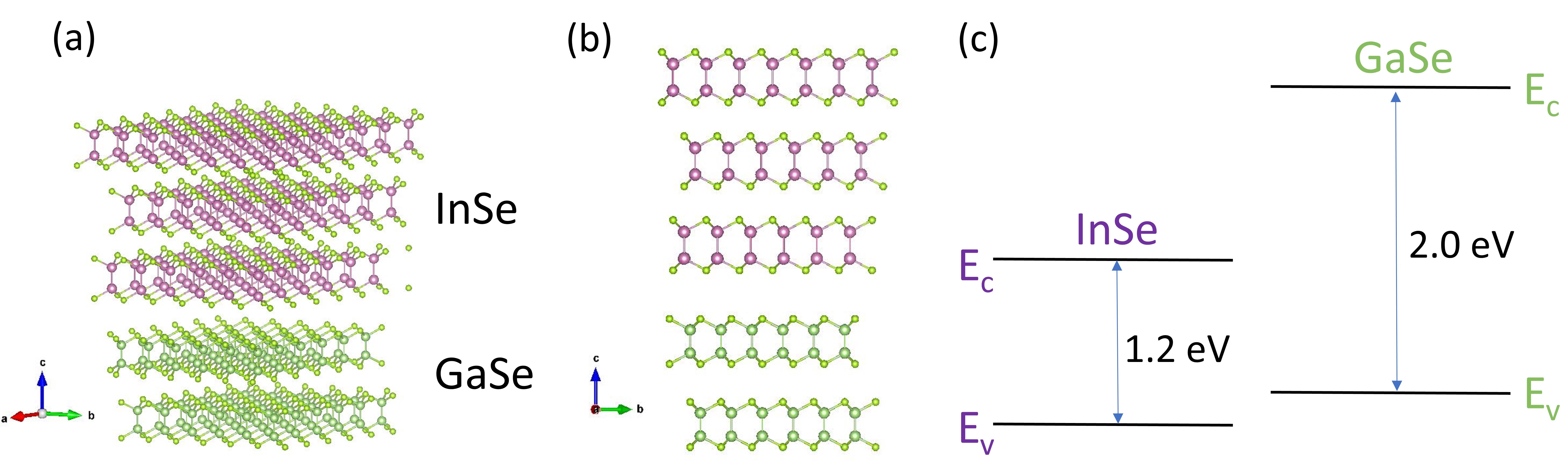
Going beyond MoS2 and TMDCs, group-III 2D monochalcogenides, represented by InSe, and GaSe, have emerged as an important family of 2D semiconductors with unique attributes. InSe has a direct band gap of 1.2 eV in the bulk and it has a layered honey-comb lattice structure with each layer containing four covalently bonded atomic planes, given by the bonding structure of Se-In-In-Se21, 22, 23, 24. The order of layer stacking gives us different polymorphs – -InSe,-InSe etc. GaSe, another group III monochalcogenide 2D semiconductor, has the same crystal structure of InSe but with a wider band-gap of 2 eV, in the bulk form (Fig.1)21. The high intrinsic electron mobility of InSe has recently attracted significant research interest for exploring fundamental physics such as high mobility 2D electron transport, quantum hall effect 22, 23, 24, 25, 26 and spin-orbit interaction 27, 28 in an atomically thin semiconductor layer. In terms of optical properties, in contrast to the TMDC family, these III-VI monochalcogenides exhibit a direct to indirect bandgap transition in the few layer thickness limit29, 24 suggesting possible device applications in opto-electronics with only a few layer thickness. Few layer InSe nanodevices were demonstrated as flexible photodetectors 30, 31 and n-InSe/p-GaSe heterostructures were shown to have potential in light emitting or photodetection devices32, 21. There is also an increasing interest in the electronic, optical and thermal properties of group-III monochalcogenide heterostructures in theory33, 34. However, the electrical transport properties of InSe/GaSe heterostructures remain largely unexplored.
In this paper, we report on the gate modulated electrical transport properties of InSe/GaSe heterostructures. Evidence for electron transfer from GaSe to InSe upon the heterostructure formation is observed in InSe FET devices supported on SiO2 after stacking few-layer GaSe on top of InSe. In devices with InSe supported on few-layer GaSe, the gating of InSe channel is shown to exhibit a strong scanning rate dependent hysteresis effect and time-dependent conductance relaxation. Such hysteretic or dynamic phenomenon is explained in the context of type II band alignment in InSe/GaSe21, 32 and gate electric field assisted charge transfer at the interface. These results provide insights on the understanding and future developments of group-III 2D monochalcogenide heterostructure electronic devices.
2 Experimental Section
For this study, InSe and GaSe bulk crystals grown by the Bridgeman method, similar to Sucharitakul et al 23. InSe and GaSe nano-flakes were exfoliated using the mechanical exfoliation method1, 2, 3. First, nanoflakes of GaSe or InSe were transferred onto degenerately doped Si substrates with a 300 nm thick SiO2 surface capping layer. To form a vertical heterostructure, e.g. InSe/GaSe heterostructure with InSe on top, a PDMS (Poly-DiMethyl-Siloxane) stamp placed on a glass slide was used to pick up an InSe nanoflake of thickness 10 nm – 60 nm and aligned with the GaSe pre-identified on the SiO2/Si substrate under a transfer stage microscope, and brought into contact. The PDMS was slowly removed, leaving the formed InSe/GaSe heterostructure on the substrate. GaSe/InSe heterostructure with InSe at the bottom can be formed in a similar way except it is the GaSe nanoflake being manipulated by the PDMS and aligned with InSe nanoflake on SiO2/Si substrate. The completed heterostructure was then annealed at 250°C under Ar/H2 atmosphere. To fabricate metal electrodes, a copper grid was used as a shadow mask, with the grid covering the active channel of the heterostructure device. 30 nm thick Ti and 60 nm thick Ni metals were then evaporated onto the masked substrate, followed by removal of the copper grid. The completed device was then annealed at 250°C under Ar/H2 atmosphere to improve contacts with the metal electrodes.
For electrical measurement at room temperature, devices were characterized in a Lakeshore Probe Station. DC source (S)-drain (D) voltage in the range 0.1-1V and gate voltages from -70V to 70V were applied to the Si substrate backgate (G) and the source-drain current was measured with a current amplifier. A Physical Property Measuring System (Quantum Design Inc.) was used for temperature dependent measurements down to 10K.
3 Results and discussion
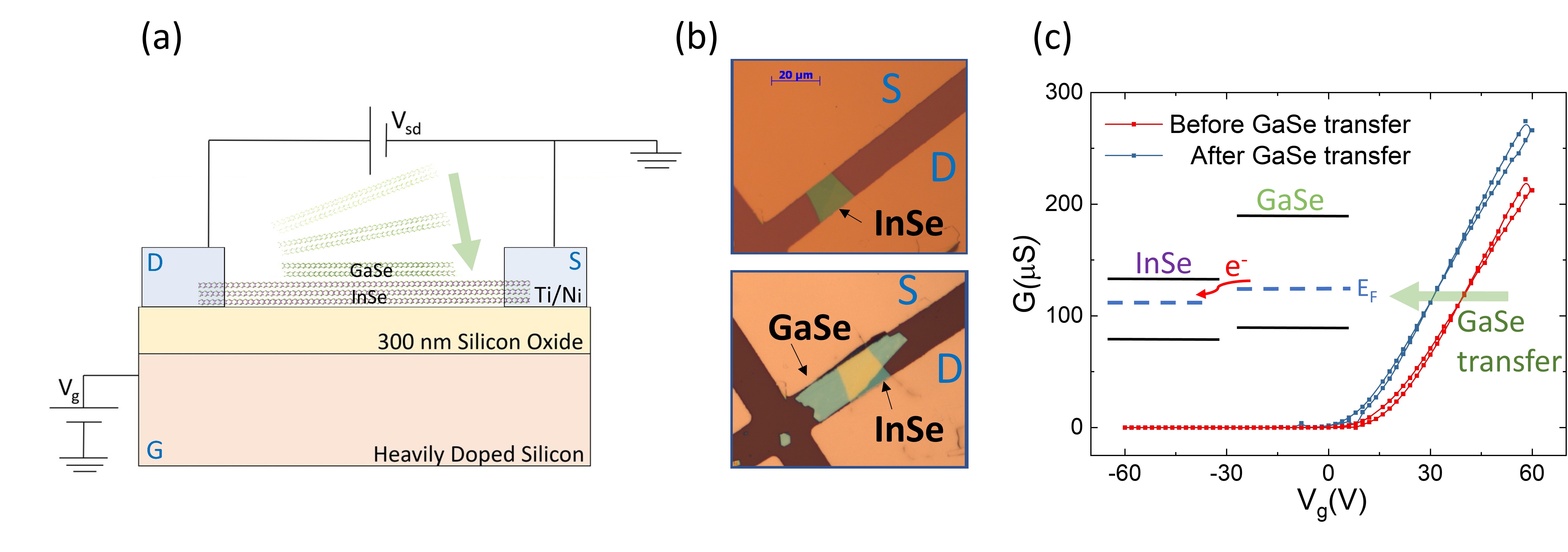
We first consider an experiment where we study the effect of the GaSe/InSe hetero-interface on InSe’s electronic property before and after the hetero-interface formation (Fig.2(a)). In this experiment, a few-layer GaSe flake was placed on top of a two-probe device with an InSe nanoflake conducting channel such that the backgate voltage is applied only through the SiO2 dielectric and we can use the gate transfer characteristics of InSe before/after the GaSe transfer to understand the influence of GaSe on InSe’s transport behavior. For this experiment, we first measured the room temperature gate-transfer characteristics in vacuum of a two-probe InSe FET device on SiO2 (Fig.2(b), top image). The measurement was done by setting the source-drain voltage (at 0.5V) and varying the backgate voltage from -70V to 70V (in steps of 2V) while measuring the source-drain current , and calculating conductance (defined as ). Afterwards, we transferred a few-layer GaSe flake onto the device using the PDMS dry-transfer technique and took care to ensure that the GaSe layer does not contact the metal electrodes (Fig.2(b), bottom image), so that conduction is still dominated by the InSe channel. The heterostructure device is then annealed in an Ar/H2 environment at 250 °C for 1 hour, to improve the hetero-interface, and gate-transfer characteristics was measured again in vacuum. We then compare the gate-transfer curves of the same InSe device before and after GaSe transfer. The device images and experimental results are shown in Fig.2 (Data for an additional sample is plotted in Fig.S1, Supplementary Info) .
From Fig.2(c), we observe a negative threshold shift of 10V following GaSe transfer, indicative of electron transfer from GaSe to InSe. The observed n-type gating behavior is typical of few-layer InSe FETs 23. Although bare GaSe nanoflakes show a p-type gating behavior (Fig.S2, Supplementary Info), the negative threshold shift upon GaSe transfer suggests that the Fermi level EF in GaSe is higher than InSe and electrons transfer from the GaSe to InSe layer upon hetero-interface formation, as illustrated in the inset of Fig.2(c). Such charge transfer is expected to cause a small band bending at the interface which will be discussed later. From the capacitance of the SiO2 dielectric layer, the charge transfer to the InSe channel is estimated from the observed threshold shift to be /cm2 (Section 5, Supplementary Info). It is interesting to point out that there is little change in the slope of gate transfer curve in Fig.2(c) after GaSe transfer, suggesting very little effect of the GaSe layer on the electron field effect mobility of InSe (estimated to be 500 cm2/Vs from the transconductance23). Besides revealing the interfacial charge transfer across the GaSe/InSe interface, this experiment also shows that the fabrication process produced high quality interface and there is a good contact between GaSe and InSe.
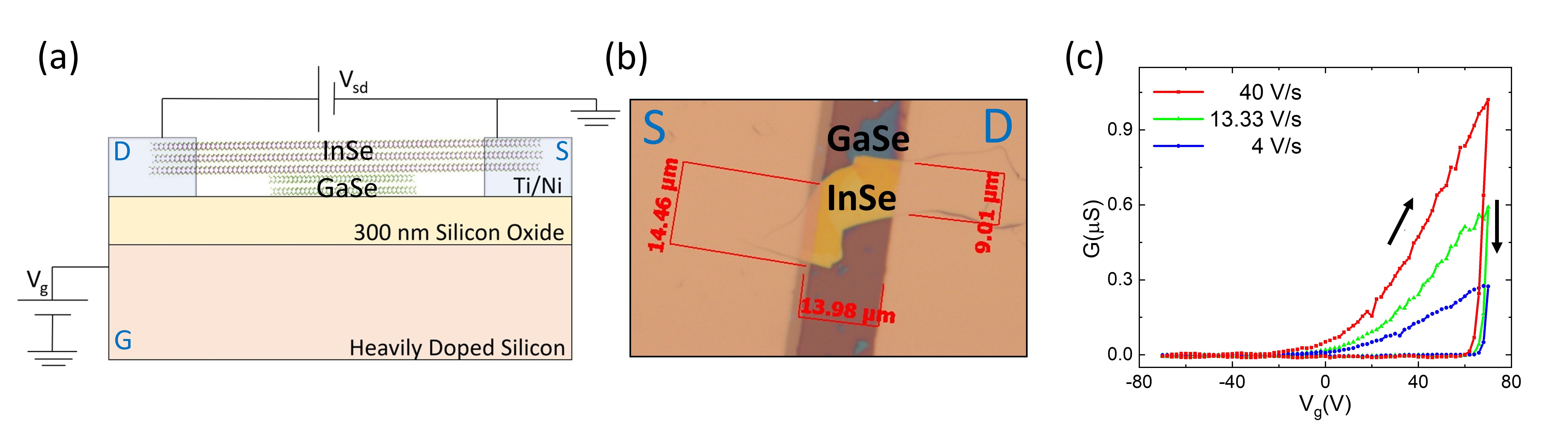
We next turn to the understanding of InSe/GaSe heterostructures when there is an external gate bias applied across the interface. Fig. 3 shows a device structure with InSe supported on top of a few-layer GaSe, where the InSe conducting channel is gated through the few-layer GaSe in addition to the SiO2 dielectric layer. The supporting GaSe layer is not in direct contact with metal electrodes, which prevents direct conduction through GaSe (Fig. 3 (a)). The gate-transfer curves for this type of devices exhibit n-type behaviour, consistent with the conduction being dominated by n-type InSe (I-V characteristics showing ohmic behavior over the range is plotted in Fig.S3 in Supplementary Info) . In contrast, we observed p-type conduction for bare GaSe (Fig. S2 in Supplementary Info). However, we see that the conductance upon gating for this type of device is two orders of magnitude lower than our bare InSe devices on SiO2 (as in Fig.2). Further, there is a strong scanning rate dependant hysteresis in the gate-transfer curves. From Fig. 3 (c) (red curve), we see that, in the direction of increasing gate voltage, the conductance increases slowly from an OFF state ( 10-2 µS) to 1 µS when changes from -20V to 70V. However, in the direction of decreasing gate voltage, the current decreases quickly from 1 µS to an OFF state within the space of 10V. This indicates a strong hysteresis effect, evidenced by a large shift in threshold voltage of 60V between the increasing and decreasing gate voltage scans. A similar hysteretic effect is seen for the different scanning rates shown in Fig. 3(c) where,in addition, we observe a strong scanning rate dependence in the gate-transfer curves with peak conductance (i.e conductance at =70V) reducing from 1 µS to 0.25 µS as the gate voltage scanning rate changes from 40 V/s to 4 V/s. These results indicate a strong time-dependant component in the gating mechanism of these heterostructure devices, which we explore further in this study. Experiments shown in Fig.3 and 4 were done in ambient atmosphere, and those in Fig.6 were done in an inert atmosphere of 6-9 Torr of He but no significant difference in the hysteresis features studied here was observed due to the effect of ambient atmosphere when compared to measurements in inert He environment or a vacuum of 50 mTorr.
Fig.4 shows the results of time-dependant conductance measurements on InSe/GaSe heterostructure devices with the structure shown in Fig.3(a). For these measurements, the source-drain voltage is fixed at 0.5V and a specific constant gate voltage is suddenly switched on and the time-dependence of the source-drain current (and hence the conductance) is measured. For the results shown in Fig. 4(a), we carry out time dependant measurements after setting =50V (from =0V). For the results shown in Fig. 4(b), we measure the time-dependence of conductance after subsequently setting gate voltages in intervals of 10V from 0-100V.
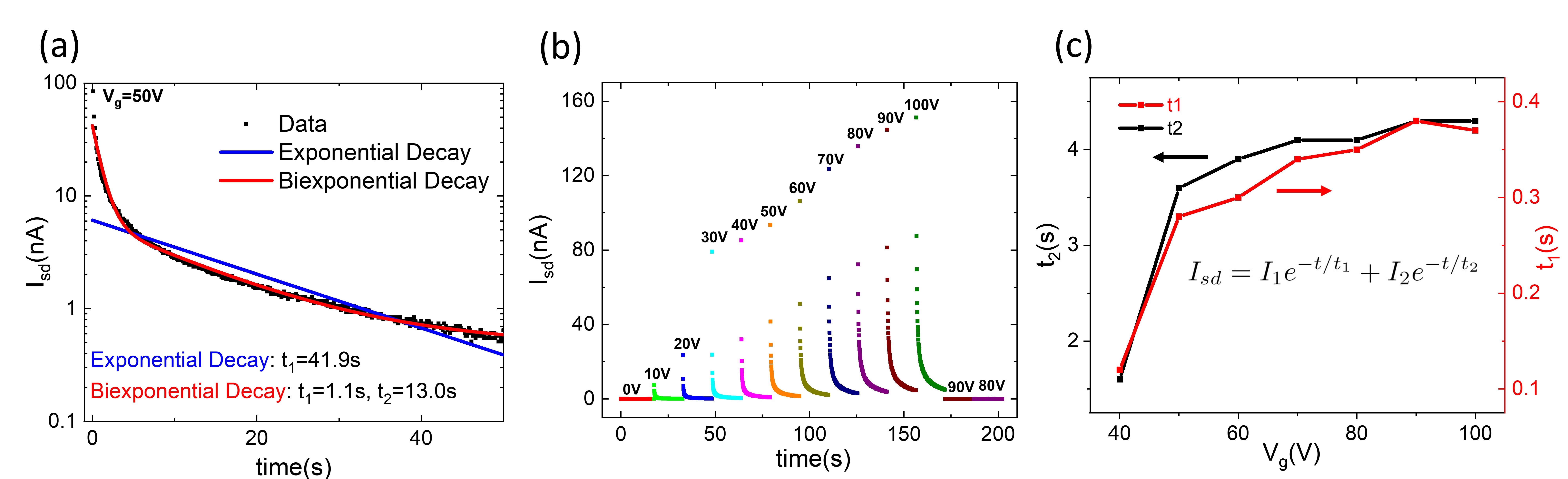
In Fig. 4(a), We observe a decay in source-drain current after setting =50V and recognize that it has good agreement with a bi-exponential decay model (equation shown in Fig. 4 (c)). In Fig. 4 (b), we observe a similar conductance decay for each gate voltage step in the increasing scanning direction, with good agreement to the bi-exponential decay equation (shown in Fig.4(c)) for 30V. The gate voltage dependence of the two time constants from the bi-exponential fit are shown in Fig.4(c). We observe that the time constants of the bi-exponential decay are of the order of 3s and 0.3s respectively, and show a gradual increase with increasing gate voltage. However, when gate voltage is decreased, a drop in conductance to a nearly zero-current OFF state is seen even at = 90V, at a rate that is much faster than the time dependence in the increasing gate voltage measurements. These observations are consistent with the scanning-rate dependant hysteretic gate-transfer curves shown in Fig.3(c).
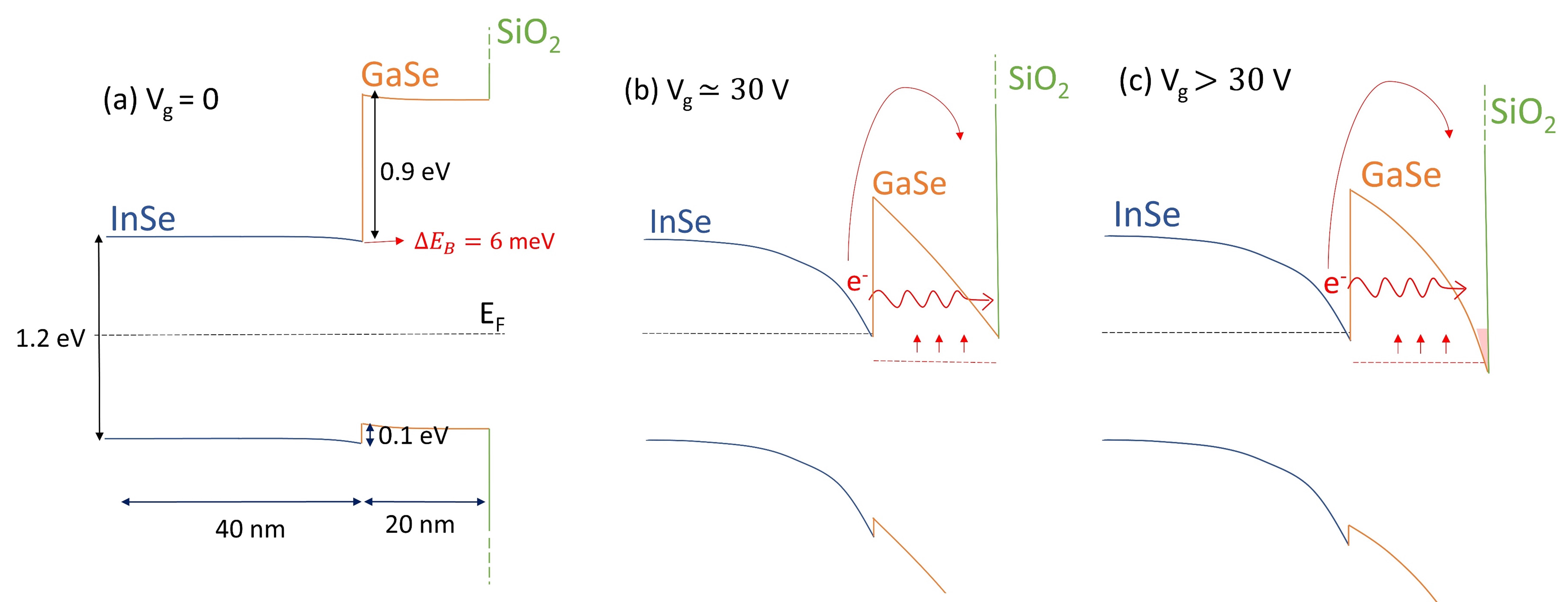
The hysteresis and time-dependent relaxation behavior suggest there is a mechanism that takes away electrons from the InSe layer when the backgate voltage is increased to transfer electrons from gate to InSe. Such mechanism is likely associated with the electron transferring from InSe to GaSe under an increasing gate bias. This also explains the much faster response of the system when the backgate voltage is decreased to transfer electrons out of InSe, since the electrons flow directly from InSe to gate in such a situation. In previous studies, n-InSe/p-GaSe heterostructures have been shown to form a Type II staggered gap band alignment, with band offsets in the conduction and valence bands determined to be approximately 0.9 eV and 0.1 eV respectively 21, 32. Close to the interface, band bending due to to equilibrium charge transfer will modify this picture, as discussed previously in the experiment shown in Fig.2. We can estimate the extent of band bending that would result from the previously estimated charge transfer of /cm2 from GaSe to InSe, by calculating the corresponding change in using the 2D density of states. We find that the band-bending at the InSe/GaSe interface to be meV (Section 5, Supplementary Info), which is insignificant compared to the band offsets. The completed band diagram relevant to our InSe/GaSe heterostructure device in Fig.3 is therefore shown in Fig.5(a) (Typical InSe and GaSe nanoflake thicknesses for our heterostructures were estimated to be 40 nm and 20 nm respectively).
Further, we quantitatively estimate the effect of applying a positive gate voltage through the SiO2 gate dielectric, on this band diagram. The gate electric field would cause the bands to tilt down, with a slope given by said electric field. At , the conduction band minimum (CBM) of InSe, tilted by electric field, is brought down to the Fermi level at the InSe/GaSe interface ( of InSe is estimated to be 0.6 eV below the CBM at =0V, see discussion in Section 5, Supplementary Info). The CBM of GaSe is also tilted downward. However, at these low gate-voltages, the CBM of GaSe is still higher than of InSe. Increasing further to , we estimate a band tilting of 0.9 eV across the 20 nm GaSe layer, which brings the CBM of GaSe at the GaSe/SiO2 interface to the level of InSe’s (Fig. 5(b)) (further details of calculation shown in Section 5, Supplementary Info). Such strong band tilting in the GaSe layer at would cause electrons accumulated in InSe to transfer into GaSe and trapped at the GaSe/SiO2 interface, giving rise to the conductance/current in InSe layer to decay with time, as shown in Fig. 5(b),(c).
We see, from Fig. 5(b), that the band diagram upon increasing the gate voltage creates a triangular potential barrier seen by electrons accumulated in InSe. There are two pathways for electrons populated in the InSe layer to transfer into the GaSe layer. The first one is through thermionic emission-like process where electrons are thermally excited above the potential barrier and the second process is direct tunneling through the barrier. These processes result in the gate voltage-induced electrons in the conducting InSe channel transferring to GaSe, leading to the observed time dependant decay in conductance after a gate voltage increase, as observed in Fig.4.
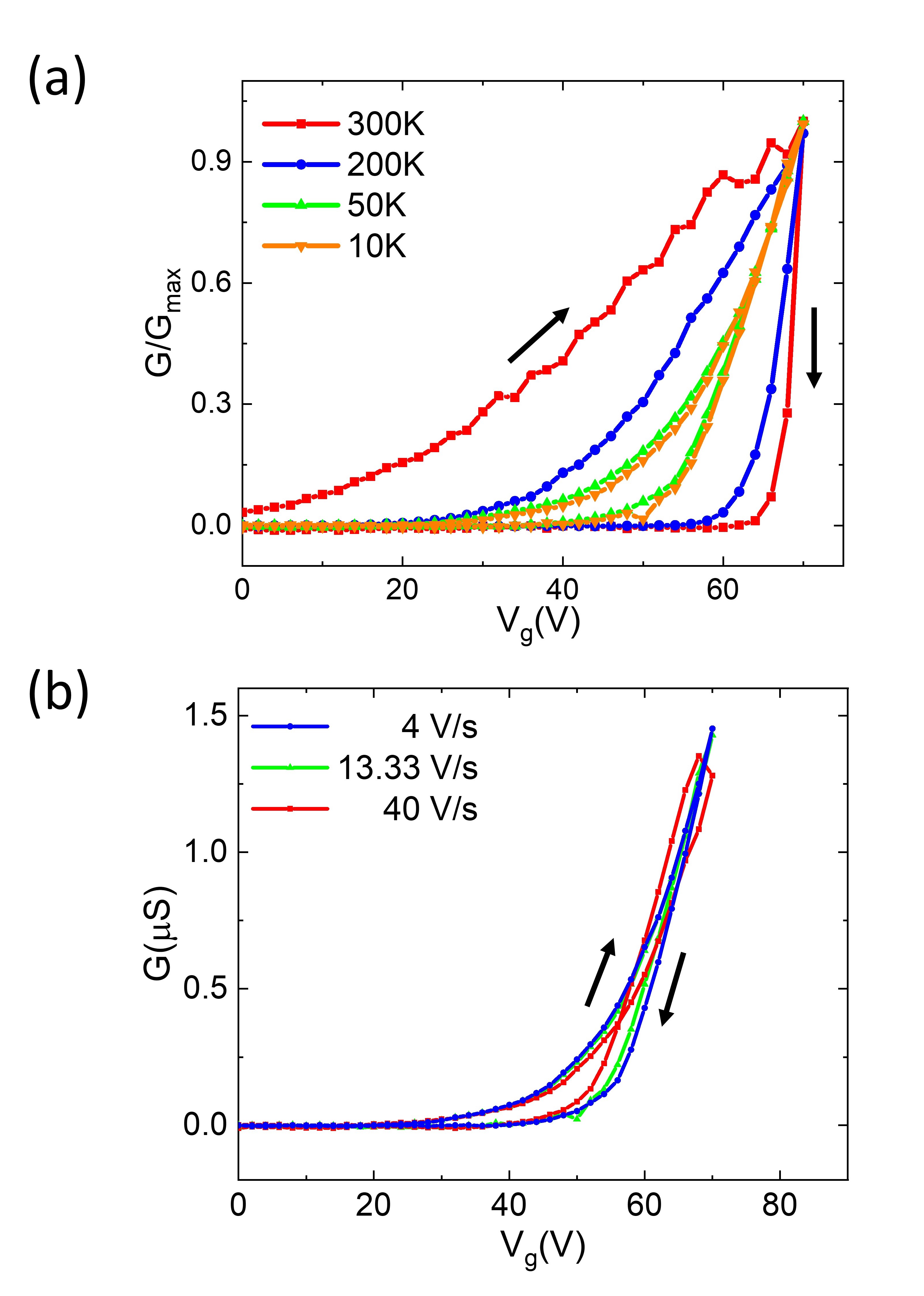
We further consider whether the relaxation time could be associated with the simple RC time constant of charging/decharging the InSe layer as the InSe channel is being depleted (via the electron transferring into GaSe). If we consider the being depleted InSe channel to have a resistance (from the current 0.5 nA at 0.5 V in Fig.4(a)) and capacitance given by (where is the gate capacitance per unit area of 300 nm SiO2 and is the area of the InSe nanoflake), this gives us a time constant s. This is significantly lesser than the measured time-constants and (Fig. 4(c)). Therefore, we conclude that the RC charging time of the circuit is not relevant to the observed bi-exponential gate-induced conductance decay. It is therefore likely that this bi-exponential decay is due to the two interfacial charge transfer processes of thermionic emission and electron tunneling across the InSe/GaSe interface. When the gate voltage is decreased, however, these processes do not play a role as the gate-induced electrons are directly pulled from the InSe channel at a much faster rate (set by the RC time constants of the circuit and measurement setup). This results in a rapid conductance decrease over a small decrease in gate voltage, and hence a large hysteresis effect in gate transfer curves, as observed in Fig.3. To further investigate the effect of thermal excitation on these observed properties, we perform temperature dependant gate-transfer measurements on these heterostructure devices down to 10K to distinguish processes that are temperature dependent (e.g. thermionic emission) or temperature-independent (e.g. tunneling). We observe, from results shown in Fig.6(a) which plots the normalized conductance vs. gate voltage at different temperatures for a fixed scanning rate, that the hysteresis effect seen at room temperature (Fig.3) becomes less at lower temperatures and only a weak residual hysteresis is seen below 50K (raw data are shown in Fig.S4 in Supplementary Information). At low temperatures, the scanning-rate of gate voltage also does not have much effect on the gate-transfer measurements as shown in Fig. 6(b) taken at 10K. This indicates that thermionic emission-like thermally assisted charge transfer process no longer plays a role at these low temperatures and any residual hysteresis observed is due to electron tunneling (which also occurs at a much lower rate at lower temperatures - see Hartman et al35, for example).
The charge transfer mechanism we have discussed in this paper is in analogy to the one discussed in Li et al 36 to explain large hysteresis in BP/hBN/MoS2 heterostructures demonstrated for non-volatile memory applications. In Li et al 36, a 25 nm layer of hBN is used to create the potential barrier across which electrons can tunnel through. In the case of our InSe/GaSe heterostructures, the InSe/GaSe band alignment creates this potential barrier, which is adjusted by the backgate voltage.
4 Conclusions
In summary, We have studied electron transport properties of InSe/GaSe heterostructures through DC transport measurements. Under static condition without an external electric field applied across the InSe/GaSe interface, we find evidence of electron transfer from GaSe to InSe layer upon the hetero-interface formation. When an external gate voltage is applied across the InSe/GaSe interface, a bi-exponential conductance decay is observed after setting a gate voltage together with a strong scanning rate dependant hysteresis effect in the gate-transfer curve. We interpret these observations through dynamical interfacial charge transfer between InSe and GaSe, mediated by gate voltage. These observations give insight into transport mechanisms in 2D van der Waal semiconductor heterostructures, and highlight the importance of band alignment in these heterostructure devices. They also open up possibilities for using InSe/GaSe heterostructure’s dynamic charge transport properties for device applications (e.g. non-volatile memory).
XPAG acknowledges the financial support from NSF (DMR-1607631) and Raman Sankar and Art Ramirez for providing some of the bulk InSe, GaSe crystals used in this work.
I-V characterization data for the InSe/GaSe heterostructure sample used in this text (Fig.3), additional data on other samples, gate-transfer curve for a bare GaSe sample, and band bending calculation details are available in Supplementary Info.
References
- Novoselov et al. 2016 Novoselov, K. S.; Mishchenko, A.; Carvalho, A.; Castro Neto, A. H. 2D materials and van der Waals heterostructures. Science (New York, N.Y.) 2016, 353, 9439
- Geim and Grigorieva 2013 Geim, A. K.; Grigorieva, I. V. Van der Waals heterostructures. Nature 2013, 499, 419–425
- Frisenda et al. 2018 Frisenda, R.; Navarro-Moratalla, E.; Gant, P.; Pérez De Lara, D.; Jarillo-Herrero, P.; Gorbachev, R. V.; Castellanos-Gomez, A. Recent progress in the assembly of nanodevices and van der Waals heterostructures by deterministic placement of 2D materials. Chemical Society Reviews 2018, 47, 53–68
- Dean et al. 2010 Dean, C. R.; Young, A. F.; Meric, I.; Lee, C.; Wang, L.; Sorgenfrei, S.; Watanabe, K.; Taniguchi, T.; Kim, P.; Shepard, K. L.; Hone, J. Boron nitride substrates for high-quality graphene electronics. Nature Nanotechnology 2010, 5, 722–726
- Dean et al. 2013 Dean, C. R.; Wang, L.; Maher, P.; Forsythe, C.; Ghahari, F.; Gao, Y.; Katoch, J.; Ishigami, M.; Moon, P.; Koshino, M.; Taniguchi, T.; Watanabe, K.; Shepard, K. L.; Hone, J.; Kim, P. Hofstadter’s butterfly and the fractal quantum Hall effect in moiré superlattices. Nature 2013, 497, 598–602
- Cui et al. 2015 Cui, X. et al. Multi-terminal transport measurements of MoS2 using a van der Waals heterostructure device platform. Nature Nanotechnology 2015, 10, 534–540
- Terrés et al. 2016 Terrés, B.; Chizhova, L. A.; Libisch, F.; Peiro, J.; Jörger, D.; Engels, S.; Girschik, A.; Watanabe, K.; Taniguchi, T.; Rotkin, S. V.; Burgdörfer, J.; Stampfer, C. Size quantization of Dirac fermions in graphene constrictions. Nature Communications 2016, 7, 11528
- Li et al. 2016 Li, J.; Wang, K.; McFaul, K. J.; Zern, Z.; Ren, Y.; Watanabe, K.; Taniguchi, T.; Qiao, Z.; Zhu, J. Gate-controlled topological conducting channels in bilayer graphene. Nature Nanotechnology 2016, 11, 1060–1065
- Cao et al. 2018 Cao, Y.; Fatemi, V.; Fang, S.; Watanabe, K.; Taniguchi, T.; Kaxiras, E.; Jarillo-Herrero, P. Unconventional superconductivity in magic-angle graphene superlattices. Nature 2018, 556, 43–50
- Zhang et al. 2016 Zhang, W.; Wang, Q.; Chen, Y.; Wang, Z.; Wee, A. T. S. Van der Waals stacked 2D layered materials for optoelectronics. 2D Materials 2016, 3, 022001
- Liu et al. 2016 Liu, Y.; Weiss, N. O.; Duan, X.; Cheng, H.-C.; Huang, Y.; Duan, X. Van der Waals heterostructures and devices. Nature Reviews Materials 2016, 1, 16042
- Lee et al. 2014 Lee, C.-H.; Lee, G.-H.; van der Zande, A. M.; Chen, W.; Li, Y.; Han, M.; Cui, X.; Arefe, G.; Nuckolls, C.; Heinz, T. F.; Guo, J.; Hone, J.; Kim, P. Atomically thin p–n junctions with van der Waals heterointerfaces. Nature Nanotechnology 2014, 9, 676–681
- Furchi et al. 2014 Furchi, M. M.; Pospischil, A.; Libisch, F.; Burgdörfer, J.; Mueller, T. Photovoltaic Effect in an Electrically Tunable van der Waals Heterojunction. Nano Letters 2014, 14, 4785–4791
- Cheng et al. 2014 Cheng, R.; Li, D.; Zhou, H.; Wang, C.; Yin, A.; Jiang, S.; Liu, Y.; Chen, Y.; Huang, Y.; Duan, X. Electroluminescence and Photocurrent Generation from Atomically Sharp WSe2 /MoS2 Heterojunction p–n Diodes. Nano Letters 2014, 14, 5590–5597
- Deng et al. 2014 Deng, Y.; Luo, Z.; Conrad, N. J.; Liu, H.; Gong, Y.; Najmaei, S.; Ajayan, P. M.; Lou, J.; Xu, X.; Ye, P. D. Black Phosphorus–Monolayer MoS2 van der Waals Heterojunction p–n Diode. ACS Nano 2014, 8, 8292–8299
- Ye et al. 2016 Ye, L.; Li, H.; Chen, Z.; Xu, J. Near-Infrared Photodetector Based on MoS2 /Black Phosphorus Heterojunction. ACS Photonics 2016, 3, 692–699
- Xue et al. 2016 Xue, Y.; Zhang, Y.; Liu, Y.; Liu, H.; Song, J.; Sophia, J.; Liu, J.; Xu, Z.; Xu, Q.; Wang, Z.; Zheng, J.; Liu, Y.; Li, S.; Bao, Q. Scalable Production of a Few-Layer MoS2 /WS2 Vertical Heterojunction Array and Its Application for Photodetectors. ACS Nano 2016, 10, 573–580
- Yu et al. 2013 Yu, W. J.; Liu, Y.; Zhou, H.; Yin, A.; Li, Z.; Huang, Y.; Duan, X. Highly efficient gate-tunable photocurrent generation in vertical heterostructures of layered materials. Nature Nanotechnology 2013, 8, 952–958
- Wang et al. 2015 Wang, F.; Wang, Z.; Xu, K.; Wang, F.; Wang, Q.; Huang, Y.; Yin, L.; He, J. Tunable GaTe-MoS2 van der Waals p–n Junctions with Novel Optoelectronic Performance. Nano Letters 2015, 15, 7558–7566
- Baugher et al. 2014 Baugher, B. W. H.; Churchill, H. O. H.; Yang, Y.; Jarillo-Herrero, P. Optoelectronic devices based on electrically tunable p–n diodes in a monolayer dichalcogenide. Nature Nanotechnology 2014, 9, 262–267
- Balakrishnan et al. 2014 Balakrishnan, N.; Kudrynskyi, Z. R.; Fay, M. W.; Mudd, G. W.; Svatek, S. A.; Makarovsky, O.; Kovalyuk, Z. D.; Eaves, L.; Beton, P. H.; Patanè, A. Room Temperature Electroluminescence from Mechanically Formed van der Waals III-VI Homojunctions and Heterojunctions. Advanced Optical Materials 2014, 2, 1064–1069
- Feng et al. 2014 Feng, W.; Zheng, W.; Cao, W.; Hu, P. Back Gated Multilayer InSe Transistors with Enhanced Carrier Mobilities via the Suppression of Carrier Scattering from a Dielectric Interface. Advanced Materials 2014, 26, 6587–6593
- Sucharitakul et al. 2015 Sucharitakul, S.; Goble, N. J.; Kumar, U. R.; Sankar, R.; Bogorad, Z. A.; Chou, F.-C.; Chen, Y.-T.; Gao, X. P. A. Intrinsic Electron Mobility Exceeding 103 cm2/(V s) in Multilayer InSe FETs. Nano Letters 2015, 15, 3815–3819
- Bandurin et al. 2017 Bandurin, D. A. et al. High electron mobility, quantum Hall effect and anomalous optical response in atomically thin InSe. Nature Nanotechnology 2017, 12, 223–227
- Ho et al. 2017 Ho, P.-H.; Chang, Y.-R.; Chu, Y.-C.; Li, M.-K.; Tsai, C.-A.; Wang, W.-H.; Ho, C.-H.; Chen, C.-W.; Chiu, P.-W. High-Mobility InSe Transistors: The Role of Surface Oxides. ACS Nano 2017, 11, 7362–7370
- Li et al. 2018 Li, M.; Lin, C.-Y.; Yang, S.-H.; Chang, Y.-M.; Chang, J.-K.; Yang, F.-S.; Zhong, C.; Jian, W.-B.; Lien, C.-H.; Ho, C.-H.; Liu, H.-J.; Huang, R.; Li, W.; Lin, Y.-F.; Chu, J. High Mobilities in Layered InSe Transistors with Indium-Encapsulation-Induced Surface Charge Doping. Advanced Materials 2018, 30, 1803690
- Premasiri et al. 2018 Premasiri, K.; Radha, S. K.; Sucharitakul, S.; Kumar, U. R.; Sankar, R.; Chou, F.-C.; Chen, Y.-T.; Gao, X. P. A. Tuning Rashba Spin–Orbit Coupling in Gated Multilayer InSe. Nano Letters 2018, 18, 4403–4408
- Zeng et al. 2018 Zeng, J. et al. Gate-tunable weak antilocalization in a few-layer InSe. Physical Review B 2018, 98, 125414
- Mudd et al. 2013 Mudd, G. W.; Svatek, S. A.; Ren, T.; Patanè, A.; Makarovsky, O.; Eaves, L.; Beton, P. H.; Kovalyuk, Z. D.; Lashkarev, G. V.; Kudrynskyi, Z. R.; Dmitriev, A. I. Tuning the Bandgap of Exfoliated InSe Nanosheets by Quantum Confinement. Advanced Materials 2013, 25, 5714–5718
- Lei et al. 2014 Lei, S.; Ge, L.; Najmaei, S.; George, A.; Kappera, R.; Lou, J.; Chhowalla, M.; Yamaguchi, H.; Gupta, G.; Vajtai, R.; Mohite, A. D.; Ajayan, P. M. Evolution of the Electronic Band Structure and Efficient Photo-Detection in Atomic Layers of InSe. ACS Nano 2014, 8, 1263–1272
- Tamalampudi et al. 2014 Tamalampudi, S. R.; Lu, Y.-Y.; Kumar U., R.; Sankar, R.; Liao, C.-D.; Moorthy B., K.; Cheng, C.-H.; Chou, F. C.; Chen, Y.-T. High Performance and Bendable Few-Layered InSe Photodetectors with Broad Spectral Response. Nano Letters 2014, 14, 2800–2806
- Yan et al. 2017 Yan, F.; Zhao, L.; Patanè, A.; Hu, P.; Wei, X.; Luo, W.; Zhang, D.; Lv, Q.; Feng, Q.; Shen, C.; Chang, K.; Eaves, L.; Wang, K. Fast, multicolor photodetection with graphene-contacted p-GaSe/ n-InSe van der Waals heterostructures. Nanotechnology 2017, 28, 27LT01
- Ibarra-Hernández et al. 2017 Ibarra-Hernández, W.; Elsayed, H.; Romero, A. H.; Bautista-Hernández, A.; Olguín, D.; Cantarero, A. Electronic structure, lattice dynamics, and optical properties of a novel van der Waals semiconductor heterostructure: InGaSe2. Phys. Rev. B 2017, 96, 035201
- Rahman et al. 2018 Rahman, A. U.; Morbec, J. M.; Rahman, G.; Kratzer, P. Commensurate versus incommensurate heterostructures of group-III monochalcogenides. Phys. Rev. Materials 2018, 2, 094002
- Hartman and Chivian 1964 Hartman, T. E.; Chivian, J. S. Electron Tunneling Through Thin Aluminum Oxide Films. Phys. Rev. 1964, 134, A1094–A1101
- Li et al. 2015 Li, D.; Wang, X.; Zhang, Q.; Zou, L.; Xu, X.; Zhang, Z. Nonvolatile Floating-Gate Memories Based on Stacked Black Phosphorus-Boron Nitride-MoS2 Heterostructures. Advanced Functional Materials 2015, 25, 7360–7365