Electronic localization in twisted bilayer MoS2 with small rotation angle
Abstract
Moiré patterns are known to confine electronic states in transition metal dichalcogenide bilayers, thus generalizing the notion of magic angles discovered in twisted bilayer graphene to semiconductors. Here, we present a revised Slater-Koster tight-binding model that facilitates the first reliable and systematic studies of such states in twisted bilayer MoS2 for the whole range of rotation angles . We show that isolated bands appear at low energy for . Moreover, these bands become “flatbands”, characterized by a vanishing average velocity, for the smallest angles .
Introduction.– Electronic correlations, i.e., the Coulomb interactions between electrons, can give rise to exotic states of matter, with notable examples including Mott insulators Mott (1949) and superconductors Bardeen et al. (1957). Some of the phenomena observed, e.g., in the so-called high-temperature superconductors Lee et al. (2006) continue to pose puzzles despite of decades of research. The discovery of electronic localization by a moiré pattern in twisted bilayer graphene Lopes dos Santos et al. (2007); Trambly de Laissardière et al. (2010); Suárez Morell et al. (2010); Bistritzer and MacDonald (2011) allows the realization of such phenomena in intrinsically only weakly correlated 2D materials thanks to the emergence of flatbands at low energies that enhances the importance of interactions. Research in this field has been boosted by the experimental discovery of correlated insulators Cao et al. (2018a) and unconventional superconducting states Cao et al. (2018b). In recent years, the broad family of transition metal dichalcogenides (TMDs) Wang et al. (2015a); Liu et al. (2015); Duong et al. (2017), which offers a wide variety of possible rotationally stacked bilayer systems, has also prompted numerous experimental van der Zande et al. (2014); Liu et al. (2014); Huang et al. (2014, 2016); Zhang et al. (2017); Trainer et al. (2017); Yeh et al. (2016); Lin et al. (2018); Pan et al. (2018); Zhang et al. (2020a) and theoretical Roldán et al. (2014); Fang et al. (2015); Cao and Li (2015); Wang et al. (2015b); Constantinescu and Hine (2015); Tan et al. (2016); Lu et al. (2017); Naik and Jain (2018); Conte et al. (2019); Maity et al. (2019); Tang et al. (2020); Wu et al. (2020); Lu et al. (2020); Xian et al. (2020); Pan et al. (2020) studies to understand such confined moiré states in semiconductor materials. Many of these studies analyze the interlayer distances, the possible atomic relaxation, the transition from a direct band gap in the monolayer system to an indirect band gap in bilayer systems, and more generally the effect of interlayer coupling in those twisted 2D systems with various rotation angles . At small values of , the emergence of flatbands has been established Naik and Jain (2018) from first-principles density functional theory calculations in twisted bilayer MoS2 (tb-MoS2), and observed in a 3∘ twisted bilayer WSe2 sample by using scanning tunneling spectroscopy Zhang et al. (2020a). Recently, it has been shown numerically Lu et al. (2020) that Lithium intercalation in tb-MoS2 increases interlayer coupling and thus promotes flatbands around the gap. There is also experimental evidence that moiré patterns may give rise to confined states due to the mismatch of the lattice parameters in MoS2-WSe2 heterobilayers Pan et al. (2018).
Most theoretical investigations of the electronic structure of bilayer MoS2 are density-functional theory (DFT) studies van der Zande et al. (2014); Liu et al. (2014); Huang et al. (2014); Zhang et al. (2017); Roldán et al. (2014); Fang et al. (2015); Cao and Li (2015); Wang et al. (2015b); Constantinescu and Hine (2015); Huang et al. (2016); Tan et al. (2016); Lu et al. (2017); Fang et al. (2015); Trainer et al. (2017); Naik and Jain (2018); Debbichi et al. (2014); Peng et al. (2014); He et al. (2014); Sun et al. (2020) with eventually a Wannier wavefunction analysis Fang et al. (2015). Those approaches provide interesting results, but they do not allow a systematic analysis of the electronic structure as a function of the rotation angle , in particular for small angles, i.e., very large moiré cells, for which DFT calculations are not feasible. Several Tight-Binding (TB) models, based on Slater-Koster (SK) parameters Slater and Koster (1954), have been proposed for monolayer MoS2 Cappelluti et al. (2013); Rostami et al. (2013); Zahid et al. (2013); Ridolfi et al. (2015); Silva-Guillén et al. (2016) and multi-layer MoS2 Cappelluti et al. (2013); Roldán et al. (2014); Fang et al. (2015); Zahid et al. (2013). Following these efforts, we propose here a Slater-Koster set of parameters that match correctly the DFT bands around the gap of tb-MoS2 with rotation angles . This SK-TB model, with the same parameters, is then used for smaller angles, in order to describe the confined moiré states. We thus show that, for , the valence band with the highest energy is separated from the other valence states by a minigap of a few meV. In addition, the width of this band decreases as decreases so that the average velocity of these electronic states reaches 0 for such that flatbands emerge at these angles. This is reminiscent of the vanishing of the velocity at certain “magic” rotation angles in bilayer graphene Lopes dos Santos et al. (2007); Trambly de Laissardière et al. (2010); Suárez Morell et al. (2010); Bistritzer and MacDonald (2011); Trambly de Laissardière et al. (2012) except that in the case of bilayer MoS2 it arises for an interval of angles. Other minigaps and flatbands are also found in the conduction band. The confined states that are closest to the gap are localized in the AA stacking regions of the moiré pattern, like in twisted bilayer graphene.
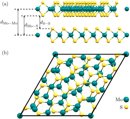
Atomic structure.– The commensurate structure of tb-MoS2 can be defined in the same manner that is common for twisted bilayer graphene (see for instance Refs. Campanera et al. (2007); Mele (2010)). Here we use the same notation as in Refs. Trambly de Laissardière et al. (2010, 2012). A commensurate tb-MoS2 with rotation angle is defined by two integers and , such that
| (1) |
and its lattice vectors are and , where ( and ( are the lattice vectors of monolayer MoS2, with the lattice distance nm. A unit cell of tb-MoS2 contains atoms. Figure 1 shows a (, ) tb-MoS2 unit cell containing 114 atoms. The cell of monolayer MoS2 contains 3 atoms: Mo at , S at and S at Huisman et al. (1971); Ridolfi et al. (2015). Note that in tb-MoS2 different types of moiré cells can be built, as the atoms of a monolayer unit cell are not equivalent by symmetry (see Supplemental Material sup , section I). For simplicity, we consider only moiré patterns constructed as follows in the main text. Starting from an AA stacked bilayer (where Mo atoms of a layer lie above the Mo atoms of the other layer, and S atoms of a layer lie above the S atoms of the other layer), the layer 2 is rotated with respect to the layer 1 by the angle around a rotation axis going through two Mo atoms. We have checked that the qualitative results presented here are also found in tb-MoS2 built from an AB stacked bilayer before rotation (see Supplemental Material sup ). The interlayer distance between layers containing Mo atoms is fixed to nm which is the DFT-optimized interlayer distance for AA stacked bilayer MoS2. The atomic relaxation probably has an important effect on the electronic structure in tb-MoS2 Naik and Jain (2018); Maity et al. (2019), like in twisted bilayer graphene Nam and Koshino (2017). However in this work, our aim is to provide a simple tight-binding (TB) scheme using Slater-Koster parameters that can be used for tb-MoS2 at all angles in order to analyze qualitatively the electronic states that are confined by the moiré pattern. Indeed, as was the case for twisted bilayer graphene, the study of the non-relaxed structure should make it possible to identify generic properties that will persist with relaxation. Therefore, our numerical results hould be qualitatively relevant even if they may not be quantitatively accurate.
DFT calculations.– The DFT Hohenberg and Kohn (1964); Kohn and Sham (1965) calculations were carried out with the ABINIT software Gonze et al. (2002, 2009, 2016) within the Monkhorst-Pack scheme Zupan et al. (1998) (more details are given in the Supplemental Material sup ). LDA Jones and Gunnarsson (1989) and GGA + Van der Waals Perdew et al. (1996) exchange-correlation functionals yield very similar results (see Fig. S4 in the Supplemental Material sup ), so all the results presented here are based on LDA calculations, which require less computation time for large systems.
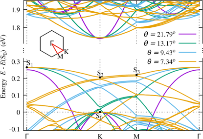
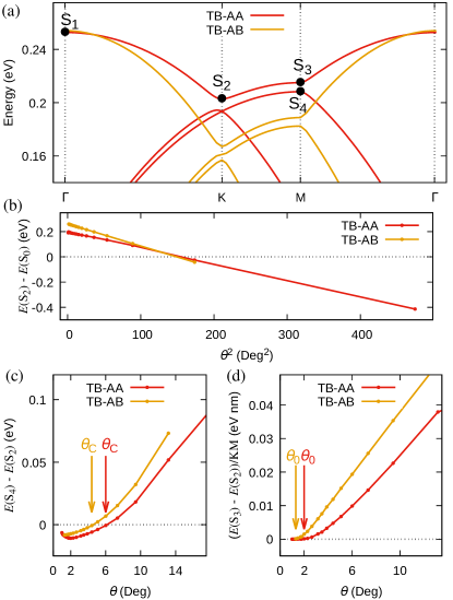
Figure 2 shows DFT bands of tb-MoS2 along symmetric lines of the first Brillouin zone for four values of the rotation angle . Note that the size of the Brillouin zones depends on the size of a unit cell of the moiré pattern such that the scale of the horizontal axis varies with . These bands should be compared with the monolayer bands plotted in the same first Brillouin zone as follows. On the one hand, some bands are not affected by the value of . Indeed, as shown in Fig. S5 of the Supplemental Material sup , the parabolic band that emanates for the point S0 is not affected by . Therefore, we always set the energy of S0 to zero. Similarly, for the angles shown in Fig. 2, the curvature of the parabola at the lowest conduction band energy at K is not affected by . On the other hand, many bands are modified with respect to the monolayer case. Like for simple stacking bilayers (AA, AB, AB’, …) Debbichi et al. (2014); Peng et al. (2014); He et al. (2014), the highest valence energy at , , increases with respect to the monolayer such that the gap becomes indirect. However, does not vary significantly with . In particular for the angles presented in Fig. 2, the curvature of the parabola at S1 is not affected by and remains close to that of the monolayer.
Finally, considering the valence band, the most spectacular effect of decreasing is the increase of the energies of some bands, thus gradually filling the gap. This is, for instance, clearly seen in Fig. 2 when considering the energy variation of the states S2 and S3 when decreases. Similarly, some energies of certain conduction bands decrease as decreases. Such a dependence of bands has already been observed for some values of the rotation angle in previous DFT calculations Naik and Jain (2018). In order to analyze it systematically, it is necessary to perform calculation for smaller angles which is difficult using DFT calculations. This is the reason why we have developed a TB model that can be used for every value of .
TB calculations.– In a first step, one needs to describe monolayer MoS2 correctly. The states around the gap at the Fermi energy are mainly 4 states of Mo Huisman et al. (1971). However, to describe valence and conduction bands correctly, it is not sufficient to restrict an effective Hamiltonian to 4 Mo orbitals. Indeed, the ligand field (S atoms) splits the 4 levels of the transition metal (Mo) atoms, and thus creates a direct gap at the K point Huisman et al. (1971). Therefore, all TB models proposed in the literature include at least 3 S orbitals Cappelluti et al. (2013); Rostami et al. (2013); Zahid et al. (2013); Ridolfi et al. (2015); Silva-Guillén et al. (2016). Roughly speaking the valence band has mainly Mo character, whereas the conduction band has character mixed with Mo character near the gap, and Mo character for higher energies Cappelluti et al. (2013). It seems that S orbitals, which have lower on-site energies, act as a perturbation of the Mo bands. For this reason, several TB models Cappelluti et al. (2013); Ridolfi et al. (2015); Silva-Guillén et al. (2016) fit rather well to the DFT band structure, while they propose very different parameters (on-site energies and Slater-Koster parameters). Our TB model for monolayer MoS2 (Fig. S3 in the Supplemental Material sup ) is an adaptation of the model proposed in Ref. Ridolfi et al. (2015) for monolayers, and is presented in detail in the Supplemental Material sup . Each unit cell of the monolayer contains 11 orbitals: 5 Mo orbitals (, , of 1 Mo atom) and 6 S orbitals (, and of 2 S atoms). Since the precise model may differ for valence and conduction states Ridolfi et al. (2015), we have decided to focus on reproducing the valence band accurately. Note that our TB model has been adapted to simulate not only the DFT monolayer bands, but also the DFT bands of twisted bilayers (mainly valence bands), as shown in the following.
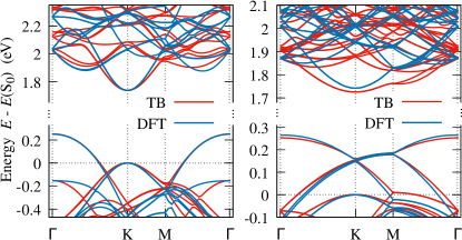
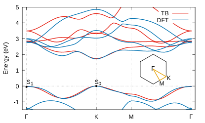
In a second step, we consider the coupling between two layers of MoS2. Most previous studies Cappelluti et al. (2013); Roldán et al. (2014); Fang et al. (2015); Zahid et al. (2013) include only interlayer coupling terms, but and terms may also be important because we do not limit the interlayer coupling to first-neighbor hopping. Therefore, we include , , and interlayer terms in our Slater-Koster scheme. It turns out that the latter two are indeed important to reproduce the DFT valence band correctly. An exponential decay with inter-atomic distance Fang et al. (2015) and a cutoff function Mehl and Papaconstantopoulos (1996) are applied to of these interlayer terms, like in twisted bilayer graphene Trambly de Laissardière et al. (2012). Figure 3 shows the comparison between DFT and TB bands for tb-MoS2 with and . The agreement is excellent for the highest energy valence bands and qualitatively correct for the conduction bands. All parameters of our TB model are given in the Supplemental Material sup .
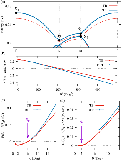
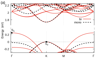
Effect of the rotation angle on bands.– We now analyze the evolution of the bands around the main gap with . Figure 4 shows this evolution for the top of the valence bands with a focus on the states labeled S1, S2, S3, and S4. Both DFT and TB results show that the energies and vary almost linearly with (Fig. 4(b)), which is a strong indication that this phenomenon is a direct consequence of the moiré structure. Indeed, in the MoS2 monolayer, the states around the gap are close to the and K points in reciprocal space, with a parabolic dispersion. In the twisted bilayer, the points and of the 2 monolayers (layer 1 and layer 2) coincide, while K1 and K2 are separated by a small distance proportional to the angle for small . As the monolayer band dispersion is parabolic, the energy of the crossing of the bands of the two layers varies with , and so do the changes in energy induced by the moiré pattern. Similarly, many studies have shown that the changes of energy due to the moiré pattern in twisted graphene bilayer varies linearly with because the low-energy bands of a graphene monolayer are linear in (see, e.g., Ref. Brihuega et al. (2012)).
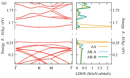
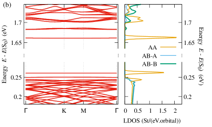
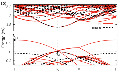
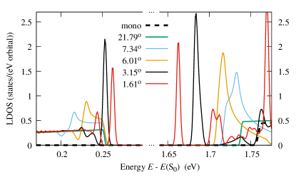
Furthermore, our TB computations show that the highest energy valence band is isolated from the remainder of the valence bands by a minigap for sufficiently small values of (Fig. 5). This is illustrated by Fig. 4(c), showing that , i.e., the presence of a minigap, for . This isolated band is not degenerate, thus it corresponds to one state per moiré cell. Figure 5 shows that such isolated bands are also present among the conduction bands with different values of . Finally, for the smallest angles, several isolated bands appear both among the valence and conduction bands.
We also consider the average slope of the highest valence band between the points K and M, i.e., between the states S2 and S3 (Fig. 4(a)). This quantity is proportional to the average Boltzmann velocity (intra-band velocity). As shown in Fig. 4(d), this velocity tends towards zero for small angles, . This demonstrates an electronic confinement corresponding to a “flatband”, like it has been found for twisted bilayer graphene for specific angles, so-called magic angles Lopes dos Santos et al. (2007); Trambly de Laissardière et al. (2010); Suárez Morell et al. (2010); Bistritzer and MacDonald (2011); Trambly de Laissardière et al. (2012). However, in tb-MoS2, this velocity vanishes not only for discrete values of , but flatbands emerge for a continuous range of , .
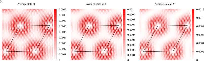
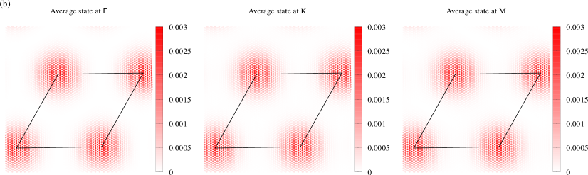
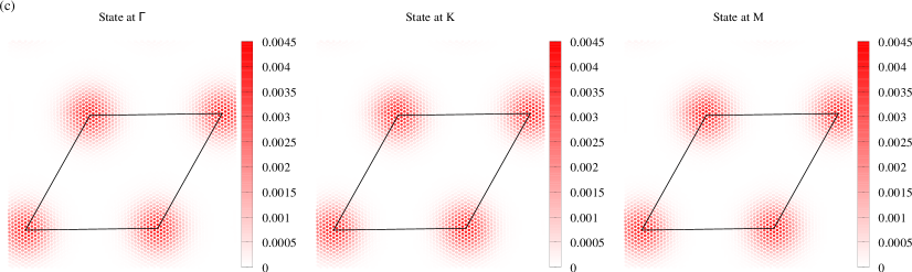
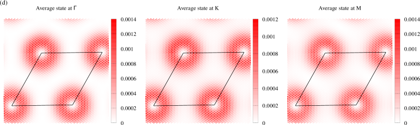
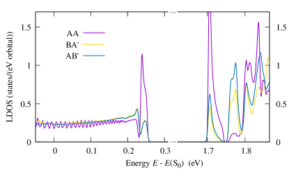
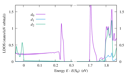
Confined state in the AA region of the moiré pattern.– Like for the monolayer, the electronic states of tb-MoS2 closest to the gap have mainly Mo character. This is still true for small angles, but states of the isolated bands are mainly localized in the AA stacking region. Consequently, the local density of states (LDOS) for Mo at the center of AA region contains sharp peaks around the gap (Fig. 5). Note that in the LDOS (Fig. 5), the minigap discussed in the previous paragraph is not seen clearly because of the numerical Gaussian broadening used to calculate the LDOS. Other figures, presented in the Supplemental Material sup , show that the sharp peaks closest to the main gap are found neither in the LDOS of the other Mo orbitals, nor in the LDOS of the Mo atoms that are not located in the AA stacking regions. Thus, the flatband states are confined in AA stacking regions, like in twisted bilayer graphene for small rotation angles Trambly de Laissardière et al. (2010); Bistritzer and MacDonald (2011); Trambly de Laissardière et al. (2012); Lopes dos Santos et al. (2012); Namarvar et al. (2020). The lowest-energy flatbands (closest to the gap in the valence and conduction bands) are localized at the center of the AA regions, as is also reflected by a strong enhancement of the local density of states in the corresponding regions (Fig. 5), whereas the next flatbands are localized in a ring in the AA regions rather than at the their center (see Fig. S9 in the Supplemental Material sup ).
Conclusion.– We have revisited the tight-binding description of twisted MoS2 bilayers starting from DFT computations. Particular attention was paid to inerlayer Slater-Koster parameters and we confirmed that not only the closest interlayer coupling terms, but also and coupling needs to be taken into account for an accurate description. We then used this tight-binding model to investigate the band structure of MoS2 bilayers at smaller rotation angles where the moiré unit cell becomes too large for DFT computations. We found that isolated bands appear in the valence and conduction bands close to the gap for . For even smaller angles , the average velocity vanishes. The emergence of the corresponding flatbands is reflected by sharp peaks in the density of states. This phenomenon is accompanied by a localization of the wave function mainly in AA stacking regions. Depending on the flatband, this real-space confinement can occur at the center of AA region and also in a ring around the center of the AA region.
In the present discussion, we have focused on rotated MoS2 bilayers that are constructed from AA stacking, but we have checked sup that qualitatively the same behavior is found when one starts from AB stacking instead.
The vanishing velocity and related emergence of flatbands identifies weakly doped MoS2 bilayers as good candidates for the observation of strong correlation effects. Beyond first theoretical efforts in this direction Xian et al. (2020), we offer our DFT-based tight-binding model as a solid starting point for more detailed studies of correlation effects in twisted MoS2 bilayers.
Note added. Recently, we were alerted of two closely related preprints Zhan et al. (2020); Zhang et al. (2020b).
Acknowledgments.– The authors wish to thank L. Magaud, P. Mallet, D. Mayou, A. Missaoui, J. Vahedi, and J.-Y. Veuillen for fruitful discussions. Calculations have been performed at the Centre de Calculs (CDC), CY Cergy Paris Université and using HPC resources from GENCI-IDRIS (grant A0060910784). We thank Y. Costes and B. Mary, CDC, for computing assistance. This work was supported by the ANR project J2D (ANR-15-CE24-0017) and the Paris//Seine excellence initiative (grant 2017-231-C01-A0).
References
- Mott (1949) N. F. Mott, “The basis of the electron theory of metals, with special reference to the transition metals,” Proc. Phys. Soc. A 62, 416–422 (1949).
- Bardeen et al. (1957) J. Bardeen, L. N. Cooper, and J. R. Schrieffer, “Theory of superconductivity,” Phys. Rev. 108, 1175–1204 (1957).
- Lee et al. (2006) P. A. Lee, N. Nagaosa, and X.-G. Wen, “Doping a Mott insulator: Physics of high-temperature superconductivity,” Rev. Mod. Phys. 78, 17–85 (2006).
- Lopes dos Santos et al. (2007) J. M. B. Lopes dos Santos, N. M. R. Peres, and A. H. Castro Neto, “Graphene bilayer with a twist: Electronic structure,” Phys. Rev. Lett. 99, 256802 (2007).
- Trambly de Laissardière et al. (2010) G. Trambly de Laissardière, D. Mayou, and L. Magaud, “Localization of Dirac electrons in rotated graphene bilayers,” Nano Letters 10, 804–808 (2010).
- Suárez Morell et al. (2010) E. Suárez Morell, J. D. Correa, P. Vargas, M. Pacheco, and Z. Barticevic, “Flat bands in slightly twisted bilayer graphene: Tight-binding calculations,” Phys. Rev. B 82, 121407(R) (2010).
- Bistritzer and MacDonald (2011) R. Bistritzer and A. H. MacDonald, “Moiré bands in twisted double-layer graphene,” Proceedings of the National Academy of Sciences 108, 12233–12237 (2011).
- Cao et al. (2018a) Y. Cao, V. Fatemi, A. Demir, S. Fang, S. L. Tomarken, J. Y. Luo, J. D. Sanchez-Yamagishi, K. Watanabe, T. Taniguchi, E. Kaxiras, R. C. Ashoori, and P. Jarillo-Herrero, “Correlated insulator behaviour at half-filling in magic-angle graphene superlattices,” Nature 556, 80 (2018a).
- Cao et al. (2018b) Y. Cao, V. Fatemi, S. Fang, K. Watanabe, T. Taniguchi, E. Kaxiras, and P. Jarillo-Herrero, “Unconventional superconductivity in magic-angle graphene superlattices,” Nature 556, 43 (2018b).
- Wang et al. (2015a) H. Wang, H. Yuan, S. Sae Hong, Y. Li, and Y. Cui, “Physical and chemical tuning of two-dimensional transition metal dichalcogenides,” Chem. Soc. Rev. 44, 2664–2680 (2015a).
- Liu et al. (2015) G.-B. Liu, D. Xiao, Y. Yao, X. Xu, and W. Yao, “Electronic structures and theoretical modelling of two-dimensional group-VIB transition metal dichalcogenides,” Chem. Soc. Rev. 44, 2643–2663 (2015).
- Duong et al. (2017) D. L. Duong, S. J. Yun, and Y. H. Lee, “van der Waals layered materials: Opportunities and challenges,” ACS Nano 11, 11803–11830 (2017).
- van der Zande et al. (2014) A. M. van der Zande, J. Kunstmann, A. Chernikov, D. A. Chenet, Y. You, X. Zhang, P. Y. Huang, T. C. Berkelbach, L. Wang, F. Zhang, M. S. Hybertsen, D. A. Muller, D. R. Reichman, T. F. Heinz, and J. C. Hone, “Tailoring the electronic structure in bilayer molybdenum disulfide via interlayer twist,” Nano Letters 14, 3869–3875 (2014).
- Liu et al. (2014) K. Liu, L. Zhang, T. Cao, C. Jin, D. Qiu, Q. Zhou, A. Zettl, P. Yang, S. G. Louie, and F. Wang, “Evolution of interlayer coupling in twisted molybdenum disulfide bilayers,” Nat. Commun. 5, 4966 (2014).
- Huang et al. (2014) S. Huang, X. Ling, L. Liang, J. Kong, H. Terrones, V. Meunier, and M. S. Dresselhaus, “Probing the interlayer coupling of twisted bilayer MoS2 using photoluminescence spectroscopy,” Nano Letters 14, 5500–5508 (2014).
- Huang et al. (2016) S. Huang, L. Liang, X. Ling, A. A. Puretzky, D. B. Geohegan, B. G. Sumpter, J. Kong, V. Meunier, and M. S. Dresselhaus, “Low-frequency interlayer Raman modes to probe interface of twisted bilayer MoS2,” Nano Letters 16, 1435–1444 (2016).
- Zhang et al. (2017) C. Zhang, C.-P. Chuu, X. Ren, M.-Y. Li, L.-J. Li, C. Jin, M.-Y. Chou, and C.-K. Shih, “Interlayer couplings, Moiré patterns, and 2D electronic superlattices in MoS2/WSe2 hetero-bilayers,” Science Advances 3, e1601459 (2017).
- Trainer et al. (2017) D. J. Trainer, A. V. Putilov, C. Di Giorgio, T. Saari, B. Wang, M. Wolak, R. U. Chandrasena, C. Lane, T.-R. Chang, H.-T. Jeng, H. Lin, F. Kronast, A. X. Gray, X. Xi, J. Nieminen, A. Bansil, and M. Iavarone, “Inter-layer coupling induced valence band edge shift in mono- to few-layer MoS2,” Scientific Reports 7, 40559 (2017).
- Yeh et al. (2016) P.-C. Yeh, W. Jin, N. Zaki, J. Kunstmann, D. Chenet, G. Arefe, J. T. Sadowski, J. I. Dadap, P. Sutter, J. Hone, and R. M. Osgood, Jr., “Direct measurement of the tunable electronic structure of bilayer MoS2 by interlayer twist,” Nano Letters 16, 953–959 (2016).
- Lin et al. (2018) M.-L. Lin, Q.-H. Tan, J.-B. Wu, X.-S. Chen, J.-H. Wang, Y.-H. Pan, X. Zhang, X. Cong, J. Zhang, W. Ji, P.-A. Hu, K.-H. Liu, and P.-H. Tan, “Moiré phonons in twisted bilayer MoS2,” ACS Nano 12, 8770–8780 (2018).
- Pan et al. (2018) Y. Pan, S. Fölsch, Y. Nie, D. Waters, Y.-C. Lin, B. Jariwala, K. Zhang, K. Cho, J. A. Robinson, and R. M. Feenstra, “Quantum-confined electronic states arising from the Moiré pattern of MoS2–WSe2 heterobilayers,” Nano Letters 18, 1849–1855 (2018).
- Zhang et al. (2020a) Z. Zhang, Y. Wang, K. Watanabe, T. Taniguchi, K. Ueno, E. Tutuc, and B. J. LeRoy, “Flat bands in twisted bilayer transition metal dichalcogenides,” Nature Physics (2020a), 10.1038/s41567-020-0958-x.
- Roldán et al. (2014) R. Roldán, J. A. Silva-Guillén, M. P. López-Sancho, F. Guinea, E. Cappelluti, and P. Ordejón, “Electronic properties of single-layer and multilayer transition metal dichalcogenides ( = Mo, W and = S, Se),” Annalen der Physik 526, 347–357 (2014).
- Fang et al. (2015) S. Fang, R. Kuate Defo, S. N. Shirodkar, S. Lieu, G. A. Tritsaris, and E. Kaxiras, “Ab initio tight-binding Hamiltonian for transition metal dichalcogenides,” Phys. Rev. B 92, 205108 (2015).
- Cao and Li (2015) B. Cao and T. Li, “Interlayer electronic coupling in arbitrarily stacked MoS2 bilayers controlled by interlayer S-S interaction,” The Journal of Physical Chemistry C 119, 1247–1252 (2015).
- Wang et al. (2015b) Z. Wang, Q. Chen, and J. Wang, “Electronic structure of twisted bilayers of graphene/MoS2 and MoS2/MoS2,” The Journal of Physical Chemistry C 119, 4752–4758 (2015b).
- Constantinescu and Hine (2015) G. C. Constantinescu and N. D. M. Hine, “Energy landscape and band-structure tuning in realistic MoS2/MoSe2 heterostructures,” Phys. Rev. B 91, 195416 (2015).
- Tan et al. (2016) Y. Tan, F. W. Chen, and A. W. Ghosh, “First principles study and empirical parametrization of twisted bilayer MoS2 based on band-unfolding,” Applied Physics Letters 109, 101601 (2016).
- Lu et al. (2017) N. Lu, H. Guo, Z. Zhuo, L. Wang, X. Wu, and X. C. Zeng, “Twisted MX2/MoS2 heterobilayers: effect of van der Waals interaction on the electronic structure,” Nanoscale 9, 19131–19138 (2017).
- Naik and Jain (2018) M. H. Naik and M. Jain, “Ultraflatbands and shear solitons in Moiré patterns of twisted bilayer transition metal dichalcogenides,” Phys. Rev. Lett. 121, 266401 (2018).
- Conte et al. (2019) F. Conte, D. Ninno, and G. Cantele, “Electronic properties and interlayer coupling of twisted MoS2/NbSe2 heterobilayers,” Phys. Rev. B 99, 155429 (2019).
- Maity et al. (2019) I. Maity, P. K. Maiti, H. R. Krishnamurthy, and M. Jain, “Reconstruction of moiré lattices in twisted transition metal dichalcogenide bilayers,” (2019), arXiv:1912.08702 [cond-mat.mtrl-sci] .
- Tang et al. (2020) Y. Tang, L. Li, T. Li, Y. Xu, S. Liu, K. Barmak, K. Watanabe, T. Taniguchi, A. H. MacDonald, J. Shan, and K. F. Mak, “Simulation of Hubbard model physics in WSe2/WS2 moiré superlattices,” Nature 579, 353–358 (2020).
- Wu et al. (2020) J. Wu, L. Meng, J. Yu, and Y. Li, “A first-principles study of electronic properties of twisted MoTe2,” physica status solidi (b) 257, 1900412 (2020).
- Lu et al. (2020) Z. Lu, S. Carr, D. T. Larson, and E. Kaxiras, “Lithium intercalation in MoS2 bilayers and implications for moiré flat bands,” (2020), arXiv:2004.00238 [cond-mat.mes-hall] .
- Xian et al. (2020) L. Xian, M. Claassen, D. Kiese, M. M. Scherer, S. Trebst, D. M. Kennes, and A. Rubio, “Realization of nearly dispersionless bands with strong orbital anisotropy from destructive interference in twisted bilayer MoS2,” (2020), arXiv:2004.02964 [cond-mat.mes-hall] .
- Pan et al. (2020) H. Pan, F. Wu, and S. Das Sarma, “Band topology, hubbard model, heisenberg model, and dzyaloshinskii-moriya interaction in twisted bilayer ,” Phys. Rev. Research 2, 033087 (2020).
- Debbichi et al. (2014) L. Debbichi, O. Eriksson, and S. Lebègue, “Electronic structure of two-dimensional transition metal dichalcogenide bilayers from ab initio theory,” Phys. Rev. B 89, 205311 (2014).
- Peng et al. (2014) T. Peng, G. Huai-Hong, Y. Teng, and Z. Zhi-Dong, “Stacking stability of MoS2 bilayer: An ab initio study,” Chinese Physics B 23, 106801 (2014).
- He et al. (2014) J. He, K. Hummer, and C. Franchini, “Stacking effects on the electronic and optical properties of bilayer transition metal dichalcogenides MoS2, MoSe2, WS2, and WSe2,” Phys. Rev. B 89, 075409 (2014).
- Sun et al. (2020) F. Sun, T. Luo, L. Li, A. Hong, C. Yuan, and W. Zhang, “Effects of magic angle on crystal and electronic structures of bilayer transition metal dichalcogenides,” (2020), arXiv:2003.09872 [cond-mat.mtrl-sci] .
- Slater and Koster (1954) J. C. Slater and G. F. Koster, “Simplified LCAO method for the periodic potential problem,” Phys. Rev. 94, 1498–1524 (1954).
- Cappelluti et al. (2013) E. Cappelluti, R. Roldán, J. A. Silva-Guillén, P. Ordejón, and F. Guinea, “Tight-binding model and direct-gap/indirect-gap transition in single-layer and multilayer MoS2,” Phys. Rev. B 88, 075409 (2013).
- Rostami et al. (2013) H. Rostami, A. G. Moghaddam, and R. Asgari, “Effective lattice Hamiltonian for monolayer MoS2: Tailoring electronic structure with perpendicular electric and magnetic fields,” Phys. Rev. B 88, 085440 (2013).
- Zahid et al. (2013) F. Zahid, L. Liu, Y. Zhu, J. Wang, and H. Guo, “A generic tight-binding model for monolayer, bilayer and bulk MoS2,” AIP Advances 3, 052111 (2013).
- Ridolfi et al. (2015) E. Ridolfi, D. Le, T. S. Rahman, E. R. Mucciolo, and C. H. Lewenkopf, “A tight-binding model for MoS2 monolayers,” J. Phys.: Condens. Matter 27, 365501 (2015).
- Silva-Guillén et al. (2016) J. Á. Silva-Guillén, P. San-Jose, and R. Roldán, “Electronic band structure of transition metal dichalcogenides from ab initio and Slater-Koster tight-binding model,” Applied Sciences 6, 284 (2016).
- Trambly de Laissardière et al. (2012) G. Trambly de Laissardière, D. Mayou, and L. Magaud, “Numerical studies of confined states in rotated bilayers of graphene,” Phys. Rev. B 86, 125413 (2012).
- Campanera et al. (2007) J. M. Campanera, G. Savini, I. Suarez-Martinez, and M. I. Heggie, “Density functional calculations on the intricacies of Moiré patterns on graphite,” Phys. Rev. B 75, 235449 (2007).
- Mele (2010) E. J. Mele, “Commensuration and interlayer coherence in twisted bilayer graphene,” Phys. Rev. B 81, 161405(R) (2010).
- Huisman et al. (1971) R. Huisman, R. de Jonge, C. Haas, and F. Jellinek, “Trigonal-prismatic coordination in solid compounds of transition metals,” Journal of Solid State Chemistry 3, 56–66 (1971).
- (52) See Supplemental Material (page 8) the commensurate moiré structures that have been used in the present work, details and complementary results on our DFT calculations, Slater-Koster parameters, and complementary tight-binding results.
- Nam and Koshino (2017) N. N. T. Nam and M. Koshino, “Lattice relaxation and energy band modulation in twisted bilayer graphene,” Phys. Rev. B 96, 075311 (2017).
- Hohenberg and Kohn (1964) P. Hohenberg and W. Kohn, “Inhomogeneous electron gas,” Phys. Rev. 136, B864–B871 (1964).
- Kohn and Sham (1965) W. Kohn and L. J. Sham, “Self-consistent equations including exchange and correlation effects,” Phys. Rev. 140, A1133–A1138 (1965).
- Gonze et al. (2002) X. Gonze, J.-M. Beuken, R. Caracas, F. Detraux, M. Fuchs, G.-M. Rignanese, L. Sindic, M. Verstraete, G. Zerah, F. Jollet, M. Torrent, A. Roy, M. Mikami, Ph. Ghosez, J.-Y. Raty, and D.C. Allan, “First-principles computation of material properties: the ABINIT software project,” Computational Materials Science 25, 478–492 (2002).
- Gonze et al. (2009) X. Gonze, B. Amadon, P.-M. Anglade, J.-M. Beuken, F. Bottin, P. Boulanger, F. Bruneval, D. Caliste, R. Caracas, M. Côté, T. Deutsch, L. Genovese, Ph. Ghosez, M. Giantomassi, S. Goedecker, D. R. Hamann, P. Hermet, F. Jollet, G. Jomard, S. Leroux, M. Mancini, S. Mazevet, M. J. T. Oliveira, G. Onida, Y. Pouillon, T. Rangel, G.-M. Rignanese, D. Sangalli, R. Shaltaf, M. Torrent, M. J. Verstraete, G. Zerah, and J. W. Zwanziger, “ABINIT: first-principles approach to material and nanosystem properties,” Comp. Phys. Commun. 180, 2582–2615 (2009).
- Gonze et al. (2016) X. Gonze, F. Jollet, F. Abreu Araujo, D. Adams, B. Amadon, T. Applencourt, C. Audouze, J.-M. Beuken, J. Bieder, A. Bokhanchuk, E. Bousquet, F. Bruneval, D. Caliste, M. Côté, F. Dahm, F. Da Pieve, M. Delaveau, M. Di Gennaro, B. Dorado, C. Espejo, G. Geneste, L. Genovese, A. Gerossier, M. Giantomassi, Y. Gillet, D. R. Hamann, L. He, G. Jomard, J. Laflamme Janssen, S. Le Roux, A. Levitt, A. Lherbier, F. Liu, I. Lukačević, A. Martin, C. Martins, M. J. T. Oliveira, S. Poncé, Y. Pouillon, T. Rangel, G.-M. Rignanese, A. H. Romero, B. Rousseau, O. Rubel, A. A. Shukri, M. Stankovski, M. Torrent, M. J. Van Setten, B. Van Troeye, M. J. Verstraete, D. Waroquiers, J. Wiktor, B. Xu, A. Zhou, and J. W. Zwanziger, “Recent developments in the ABINIT software package,” Comp. Phys. Commun. 205, 106–131 (2016).
- Zupan et al. (1998) A. Zupan, P. Blaha, K. Schwarz, and J. P. Perdew, “Pressure-induced phase transitions in solid Si, SiO2, and Fe: Performance of local-spin-density and generalized-gradient-approximation density functionals,” Phys. Rev. B 58, 11266–11272 (1998).
- Jones and Gunnarsson (1989) R. O. Jones and O. Gunnarsson, “The density functional formalism, its applications and prospects,” Rev. Mod. Phys. 61, 689–746 (1989).
- Perdew et al. (1996) J. P. Perdew, K. Burke, and M. Ernzerhof, “Generalized gradient approximation made simple,” Phys. Rev. Lett. 77, 3865–3868 (1996).
- Mehl and Papaconstantopoulos (1996) M. J. Mehl and D. A. Papaconstantopoulos, “Applications of a tight-binding total-energy method for transition and noble metals: Elastic constants, vacancies, and surfaces of monatomic metals,” Phys. Rev. B 54, 4519–4530 (1996).
- Brihuega et al. (2012) I. Brihuega, P. Mallet, H. González-Herrero, G. Trambly de Laissardière, M. M. Ugeda, L. Magaud, J. M. Gómez-Rodríguez, F. Ynduráin, and J.-Y. Veuillen, “Unraveling the intrinsic and robust nature of van Hove singularities in twisted bilayer graphene by scanning tunneling microscopy and theoretical analysis,” Phys. Rev. Lett. 109, 196802 (2012).
- Lopes dos Santos et al. (2012) J. M. B. Lopes dos Santos, N. M. R. Peres, and A. H. Castro Neto, “Continuum model of the twisted graphene bilayer,” Phys. Rev. B 86, 155449 (2012).
- Namarvar et al. (2020) O. F. Namarvar, A. Missaoui, L. Magaud, D. Mayou, and G. Trambly de Laissardière, “Electronic structure and quantum transport in twisted bilayer graphene with resonant scatterers,” Phys. Rev. B 101, 245407 (2020).
- Zhan et al. (2020) Z. Zhan, Y. Zhang, G. Yu, F Guinea, J. Á. Silva-Guillén, and S. Yuan, “Multi-ultraflatbands tunability and effect of spin-orbit coupling in twisted bilayer transition metal dichalcogenides,” (2020), arXiv:2005.13868 [cond-mat.mes-hall] .
- Zhang et al. (2020b) Y. Zhang, Z. Zhan, F. Guinea, J. Á. Silva-Guillén, and S. Yuan, “Tuning band gaps in twisted bilayer MoS2,” (2020b), arXiv:2005.13879 [cond-mat.mes-hall] .
Supplemental Material
In this Supplemental Material, we first (section I) present the commensurate moiré structures of twisted bilayer MoS2 (tb-MoS2) that have been used in the present work. Section II gives some details and complementary results on our DFT calculations. Section III provides the Tight-Binding (TB) Slater-Koster parameters for tb-MoS2. Complementary TB results (bands, local density of states, and eigenstates) are presented in section IV.
I tb-MoS2 commensurate structures
The atomic structure of commensurate twisted bilayer MoS2 (tb-MoS2) is explained in the main text. The structures of tb-MoS2 that have been used in the present work are listed table S1.
In tb-MoS2, different types of moiré patterns can be built since the atoms of a monolayer unit cell are not equivalent by symmetry. For our study we consider two kinds of moiré patterns:
-
•
Patterns from AA: Starting from an AA stacked bilayer (where Mo atoms of a layer lie above a Mo atom of the other layer, and S atoms of a layer lie above an S atom of the other layer), the layer 2 is rotated with respect to layer 1 by the angle around an axis containing two Mo atoms.
-
•
Patterns from AB: Starting from an AB stacked bilayer (were Mo atoms of layer 1 lie above a Mo atom of layer 2, and S atoms of each layer do not lie above an atom of the other layer), layer 2 is rotated with respect to layer 1 by the angle around an axis containing two Mo atoms.
For simplicity, in the main text we discussed only moiré patterns built from AA stacking, but results for moiré patterns built from AB stacking yield similar results, as shown here.
| () | [deg.] | |
|---|---|---|
| (1,2) | 21.787 | 42 |
| (2,3) | 13.174 | 114 |
| (3,4) | 9.430 | 222 |
| (4,5) | 7.341 | 366 |
| (5,6) | 6.009 | 546 |
| (6,7) | 5.086 | 762 |
| (7,8) | 4.408 | 1014 |
| (10,11) | 3.150 | 1986 |
| (15,16) | 2.134 | 4326 |
| (16,17) | 2.004 | 4902 |
| (18,19) | 1.788 | 6162 |
| (19,20) | 1.696 | 6846 |
| (20,21) | 1.614 | 7566 |
| (22,23) | 1.470 | 9114 |
| (25,26) | 1.297 | 11706 |
| (27,28) | 1.203 | 13614 |
| (30,31) | 1.085 | 16746 |
| (33,34) | 0.987 | 20202 |
| (36,37) | 0.906 | 23982 |
I.1 Moiré pattern from AA
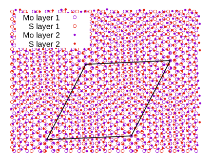
Figure S1 shows a top view of the atomic structure of tb-MoS2 built from AA stacking. One can identify several specific types of stacking regions:
-
•
AA stacking regions are regions where Mo atoms of a layer lie above a Mo atom of the other layer, and S atoms of a layer lie above an S atom of the other layer.
-
•
AB’ stacking regions are regions where Mo atoms of layer 1 lie above an S atom of layer 2, and S atoms of layer 1 (Mo atoms of layer 2) do not lie above an atom of layer 2 (layer 1).
-
•
BA’ stacking regions are regions where S atoms of layer 1 atoms lie above a Mo atom of layer 2, and Mo atoms of layer 1 (S atoms layer 2) do not lie above an atom of layer 2 (layer 1).
In Fig. S1, AA stacking regions are located at the corners of the moiré cell. BA’ and AB’ stacking regions are located at and of its long diagonal, respectively.
I.2 Moiré pattern from AB
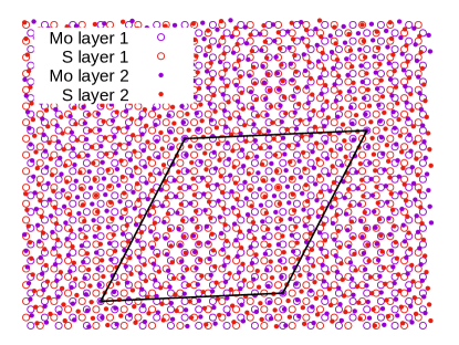
Figure S2 shows a top view of the atomic structure of tb-MoS2 built from AB stacking. Here one can identify several specific types of stacking regions:
-
•
AA’ stacking regions are regions where Mo atoms (S atoms) of one layer lie above an S atom (Mo atom) of the other layer.
-
•
AB stacking regions are regions where Mo atoms of layer 1 lie above a Mo atom of layer 2, and S atoms of each layer do not lie above an atom of the other layer.
-
•
BA stacking regions are regions where S atoms of layer 1 lie above an S atom of layer 2, and Mo atoms each layer do not lie above an atom of the other layer.
In Fig. S2, AB stacking regions are located at the corners of the moiré cell. AA’ and BA stacking regions are located at and of its long diagonal, respectively.
II DFT tb-MoS2 bands
Density functional theory (DFT) Hohenberg and Kohn (1964); Kohn and Sham (1965) calculations based on first-principle calculations were carried out with the ABINIT code Gonze et al. (2002, 2009, 2016), using the local density approximation (LDA) exchange-correlation functional Jones and Gunnarsson (1989) and the Perdew-Burke-Ernzerhof (PBE) parametrized generalized gradient approximation (GGA) exchange-correlation functional Perdew et al. (1996). We considered fourteen valence electrons of Mo , six valence electrons of S in the PAW-PBE pseudopotential. The Brillouin zone was sampled by a k-point mesh of 0.8 nm-1 separation in reciprocal space within the Monkhorst-Pack scheme Zupan et al. (1998), and the kinetic energy cutoff was chosen to be 544.22 eV. A vacuum region of 2 nm was inserted between the MoS2 bilayers to avoid spurious interactions between periodic images.
Figure S3 shows our DFT results for the band structure of monolayer MoS2. The highest energy of the valence band (state S0 at the point K) is fixed to zero, . Since the highest valence energy at the point (state S1) has a lower energy, the gap is direct, as expected Huisman et al. (1971).
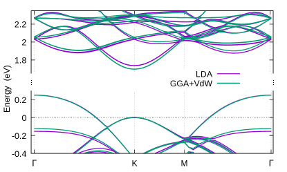
Figure S4 shows that LDA and GGA + Van der Waals approximations yield very similar results, so all further result are based on LDA calculations.
In Fig. S5, we compare the bands around the gap of and tb-MoS2 with the monolayer case. For the purpose of comparison, the monolayer unit cell has been mapped to the bilayer one.
III Tight-Binding (TB) model
In this section, we present details of our Tight-Binding (TB) Hamiltonian for monolayer MoS2 and twisted bilayer MoS2. We use a Slater-Koster scheme Slater and Koster (1954) in order to describe all the studied structures by a single set of parameters.
III.1 TB model for monolayer MoS2
We start by describing a single layer of 2H-MoS2. The lattice vectors of monolayer MoS2 are ( and (, with the lattice parameter nm. A unit cell contains 3 atoms: Mo at , S at and S at Huisman et al. (1971); Ridolfi et al. (2015).
Our TB model includes 11 orbitals per unit cell of the monolayer: 5 Mo orbitals (, , of 1 Mo atom) and 6 S orbitals (, and of 2 S atoms). By symmetry, the 2 () orbitals of each Mo are equivalent as well as the and of each S.
| Atom | Orbitals | On-site energy (eV) |
|---|---|---|
| Mo | ||
| S | , | |
| Atom | Neighbor | Number | Inter-atomic | Slater-Koster |
| distance (nm) | parameters (eV) | |||
| Mo | Mo | 3 | 0.318 | |
| S | 6 | 0.241 | ||
| S | S | 1 | 0.312 | |
| 6 | 0.318 | |||
Our TB model for monolayer MoS2 is an adaptation of the model proposed in Ref. Ridolfi et al. (2015) to our DFT results (Fig. S3). The , and hopping terms are calculated using a Slater-Koster formula with the parameters , , , , , , . For the monolayer, only first neighbor S-S, Mo-Mo and S-Mo hopping terms are taken into account. On-site energy values, number of neighbors taken into account, and values of Slater-Koster parameters are listed table S2.
III.2 TB model of twisted bilayer MoS2 (tb-MoS2)
| Atom | Neighbor | (nm) | Slater-Koster | |
| parameters (eV) | ||||
| Mo | Mo | 0.6800 | 11.6496 | |
| S | 0.5238 | 8.9738 | ||
| S | S | 0.3676 | 6.2981 | |
Now we move to tb-MoS2 where we take the monolayer MoS2 hopping terms of table S2 as the intralayer hopping terms. Most previous studies Cappelluti et al. (2013); Roldán et al. (2014); Fang et al. (2015); Zahid et al. (2013) include only interlayer hopping terms. At first sight, this may appear justified since these correspond to the shortest interlayer distance, see Fig. 1. However, and in particular are not that much bigger than such that a sharp cutoff at the shortest distance may not be appropriate. Indeed, terms and terms may also be important because we do not limit the interlayer coupling to first-neighbor hopping. Therefore, we include , , and interlayer hopping terms in our Slater-Koster scheme. Following other studies of twisted bilayer TMDCs Fang et al. (2015) and twisted bilayer graphene Trambly de Laissardière et al. (2010, 2012), each interlayer Slater-Koster parameter is assumed to decrease exponentially as a function of the distance between orbitals:
| (2) |
where the is S-S , S-S , Mo-Mo , Mo-Mo , Mo-Mo , Mo-S , Mo-S , respectively; is the corresponding interlayer distance , , and , respectively (see Fig. 1). The coefficients are fixed, like in twisted bilayer graphene Trambly de Laissardière et al. (2012), to have a reduction by a factor 10 between first neighbor hopping and second neighbor hopping terms,
| (3) |
Numerical values of , and are listed table S3.
IV TB electronic structure of tb-MoS2
IV.1 Analysis of the bands in tb-MoS2 built from AB stacking
In the main text we showed only results for tb-MoS2 built from AA stacking (see section I.1). However, other types of moiré patterns exist in this system as well; in particular, one can start from AB stacking (see section I.2). Figure S6 presents a comparison of the -dependence of the band structure between tb-MoS2 between bilayers built from AA stacking and from AB stacking. The results are qualitatively very similar, which shows that the main results of our study do not depend on the type of moiré pattern. The main quantitative differences with respect to the results discussed in the main text are the values of and : versus for tb-MoS2 built from AA and AB stacking, respectively; versus for tb-MoS2 built from AA and AB stacking, respectively.
IV.2 Local density of states (LDOS)
The TB density of states (DOS) is calculated employing a Gaussian broadening with a standard deviation meV. For the -integration we use a grid with points in the reciprocal unit cell, with large enough to obtain a DOS that is independent of these parameters. Due to this broadening, the minigaps found in the band structure are not always seen clearly in the DOS.
Figure S7 shows the LDOS for the orbital of an Mo atom at the center of the AA stacking region for several rotation angles . Figure S8 (top panel) shows the local density of states (LDOS) of the Mo orbital for the selected rotation angle , but for Mo atoms located at different stacking regions of the moiré pattern (see section I). Confined states (“flat bands”) lead to sharp peaks in the LDOS (Fig. S7). These states have Mo character (Fig. S8 (bottom panel)), and a very small weight for the other Mo orbitals. The flat bands are mainly located in the AA stacking region (Figs. S8 (top panel) and S9). Figure S9 shows that the lowest-energy flat bands in the conduction and valence bands correspond to Mo atoms that are located at the center of the AA stacking regions, and that the next flat band in the conduction and valence bands corresponds to states located in a ring in the AA stacking regions.
IV.3 Eigenstates corresponding to flat bands in tb-MoS2
Analysis of the band dispersion (Fig. 5) shows that the first isolated flat band below the main gap (valence band) is non-degenerate and thus contains one state per moiré cell. By contrast, the two first isolated flat bands above the gap (conduction bands) are two-fold quasi degenerate. The weight of the eigenstates corresponding to these flat bands is mainly concentrated on Mo orbitals (more than 98% and 95%, respectively) located at the center of AA stacking regions. This is shown in Fig. S9(b,c) for eigenstates at the points , K, and M of the flat band above and below the main gap, respectively.
For small enough angles, the next isolated flat bands (Fig. 5(b)) are four-fold quasi degenerate in the conduction band and two-fold quasi degenerate in the valence band. The weight of the eigenstates, corresponding to these flat bands at the points , K, and M, is mainly located in a ring in AA stacking regions (Fig. S9(a,d)).