The optical signature of few-layer ReSe2
Abstract
Optical properties of thin layers of rhenium diselenide (ReSe2) with thickness ranging from mono- (1 ML) to nona-layer (9 MLs) are demonstrated. The photoluminescence (PL) and Raman scattering were measured at low (=5 K) and room (=300 K) temperature, respectively. The PL spectra of ReSe2 layers display two well-resolved emission lines, which blueshift by about 120 meV when the layer thickness decreases from 9 MLs to a monolayer. A rich structure of the observed low-energy Raman scattering modes can be explained within a linear chain model. The two phonon modes of intralayer vibrations, observed in Raman scattering spectra at about 120 cm-1, exhibit very sensitive and opposite evolution as a function of layer thickness. It is shown that their energy difference can serve as a convenient and reliable tool to determine the thickness of ReSe2 flakes in the few-layer limit.
I Introduction
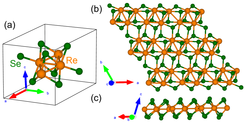
Semiconducting transition metal dichalcogenides (S-TMDs) such as MoS2, MoSe2, WS2, WSe2 and MoTe2 invariably attract attention due to their unique electronic structures and resulting optical properties Koperski et al. (2017); Wang et al. (2018). Recently, rhenium based compounds (ReS2 and ReSe2) with their weak interlayer coupling and in-plane anisotropy, have emerged as intensively investigated members of the S-TMDs family. Like other S-TMDs, ReSe2 crystals are layered materials composed of covalently bonded monolayers stacked together by weak van der Waals interactions. Each monolayer, made up of three atomic planes (Se-Re-Se), crystallizes in a distorted 1T (1T) phase with triclinic symmetry Jariwala, Thamizhavel, and Bhattacharya (2017); Lamfers et al. (1996). The schematic representation of the 1T-ReSe2 is demonstrated in Fig. 1. Its anisotropic optical and electronic properties can be utilized to produce field-effect transistors Pradhan et al. (2018); Yang et al. (2014a); Corbet et al. (2016) and photodetectors Yang et al. (2014b); Zhang et al. (2016). Moreover, it is reported that thin layer of ReSe2 may be also used to fabricate ReS2/ReSe2 heterojunction functioning as diodes or solar cellsCho et al. (2017).
The S-TMDs investigation usually starts with the identification of the atomically thin layer. The most common example of a respective tool is based on the Raman scattering spectrum. For instance the energy difference between the in-plane (A1g) and out-of-plane (E ) phonon modes in thin layers of MoS2, which strongly depends on the layer thickness Lee et al. (2010), enables their correct determination.
To create a similar tool to distinguish between layers of different thicknesses we have explored optical properties of ReSe2 from mono- (1 ML) to nona-layers (9 MLs). We performed photoluminescence (PL) and Raman scattering (RS) measurements at low (=5 K) and room (=300 K) temperature, respectively. The nature of the band structure of this material remains an open question due to inconsistent results obtained by different groups Gehlmann et al. (2017); Aslan et al. (2016); Hart et al. (2017); Arora et al. (2017). Here, we present the low-temperature PL spectra with two well-resolved emission lines, which experience a blueshift of about120 meV with decreasing the number of layers from 9 to 1. This result seems to confirm that the energy gap is direct and increases with the decrease of the layer thickness. The most common and convenient method of characterization of 2D materials is Raman spectroscopy. One of the most accurate means of determining thickness is the analysis of low-frequency interlayer phonons. Chen et al. (2015); Lorchat, Froehlicher, and Berciaud (2016); Grzeszczyk et al. (2016); Froehlicher et al. (2018) Our results present the evolution of low-energy Raman scattering modes with the layer thickness, which we address with a simple linear chain model. However, the ultra-low energy range required to measure these features is not easily accessible. For this reason, we have drawn our attention to the higher energy range, were multiple phonon peaks can be observed in RS spectra. Among them, the energies of two phonon modes of intralayer vibrations, apparent at about 111 cm-1 and 120 cm-1, exhibit very sensitive thickness dependence. The energy difference between these two peaks decreases from around 12 cm-1 for 1 ML to almost 6 cm-1 in 7-9 MLs, which may provide a convenient and reliable tool for determining flake thickness in thin layers of ReSe2. We note that this behavior is similar to that observed in ReS2. Chenet et al. (2015)
II Experimental details
Monolayer and few-layer flakes of ReSe2 were obtained on a Si/(90 nm) SiO2 substrate by polydimethylsiloxane-based exfoliation Castellanos-Gomez et al. (2014) of bulk crystals purchased from HQ Graphene. The flakes of interest were initially identified by visual inspection under an optical microscope.
The PL and RS measurements were performed using =515 nm (2.41 eV) and =633 nm (1.96 eV) radiation from continuous wave Ar-ion and He-Ne lasers, respectively. The excitation light in those experiments was focused by means of a 100x long-working distance objective with a 0.55 numerical aperture (NA) producing a spot of about 1 m diameter. The signal was collected via the same microscope objective, sent through 0.75 m monochromator, and then detected by using a liquid nitrogen cooled charge-coupled device (CCD) camera. The spectral resolution of our setup in studied energy range of the RS experiment is equal to 0.7 cm-1. To detect low-energy RS down to about 5 cm-1 from the laser line, a set of Bragg filters was implemented in both excitation and detection paths. The low-temperature PL measurements were performed with the samples placed on a cold finger in a continuous flow cryostat mounted on - manual positioners. The excitation power focused on the sample was kept at 200 W during all measurements to avoid local heating.
III Experimental results
One of the most recognizable features of molybdenum- and tungsten-based S-TMDs is indirect to direct bandgap crossover in the single-layer limit. However, the S-TMD family also includes materials that do not follow the tendency. One such group are Re-based compounds, namely ReSe2 and ReS2. It was shown that both of these materials behaved like a stack of electronically and vibrationally decoupled monolayers even in bulk form, with their optical properties being almost independent of the number of layers Tongay et al. (2014); Chenet et al. (2015); Yang et al. (2014a). In order to examine the ReSe2 thickness evolution of the band structure, we measured the low-temperature PL spectra of flakes consisting of 1 ML up to 9 MLs, presented in Fig. 2(a). The emission spectra comprise two well-resolved peaks referred to as X1 (at lower energy) and X2 (at higher energy). The X1 and X2 lines correspond to the radiative recombination of excitons comprising electrons from the bottom of the conduction band and holes from the top of the valence band. Both of the bands are 2-fold degenerate with each degenerate pair consisting of bands with opposite spins (see Refs 15; 23 for details). The excitonic emission peaks shift towards lower energies when the layer thickness is increased, from about 1.51 eV for 1 MLs to 1.39 eV for 9 MLs (see Fig. 2(b)). Moreover, the energy separation between the X1 and X2 peaks () decreases substantially with the increasing number of layers, from about 55 meV for monolayer to almost 20 meV for 9 MLs. The observed evolution of the PL peaks is compared with results of previous low-temperature transmission measurements of thin ReSe2 flakes exfoliated on sapphire substrates demonstrated in Ref. 15. As can be appreciated in Fig. 2(b), the agreement between results obtained from two different types of experiments is quite good. This strongly suggests that the origin of these two investigated transitions is the same in both the emission and absorption measurements.
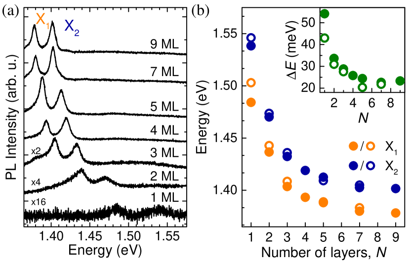
Analogous low-temperature PL spectra were measured on thin layers of ReS2 Jadczak et al. (2019). Those spectra also comprise two well-defined peaks. Their energies redshift by about 150 meV, when the layer thickness is increased from a monolayer to 15 layers. That redshift is also accompanied by a decrease of around 30 meV. The evolution is very similar to that shown in Fig. 2(b), where the corresponding numbers are of the order of 120 meV and 55 meV. These results reveal similar optical and vibrational properties of ReSe2 and ReS2, which crystallize in the same distorted 1T diamond-chain structure.
The particular 1T crystalline structure with reduced symmetry, compared to other commonly studied 2H-stacked S-TMDs Lee et al. (2010); Grzeszczyk et al. (2016), affects not only the band structure of ReSe2 but also its vibrational properties. The ReSe2 ML belongs to point group Ci, which has only an inversion symmetry Choi et al. (2020); Froehlicher et al. (2018). The unit cell of ReSe2 ML contains 12 atoms, and the irreducible representation can be written as = 18(A+A) Choi et al. (2020). This gives rise to the equal number (18) of Raman- and infrared-active modes characterized by the A and A symmetries, respectively.
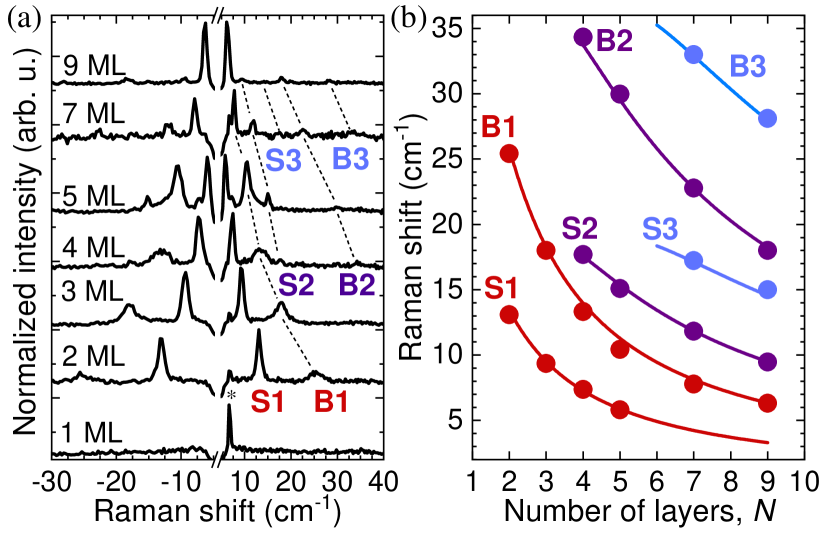
We start our analysis with measurements of low-energy (40 cm-1) RS modes, The results of the measurements are presented in Fig. 3(a). The observed peaks result from rigid interlayer vibrations of the ReSe2 layers. There are two families of the vibrations: shear and breathing modes. They are related to interlayer displacements which are perpendicular and parallel to the crystal -axis respectively. There are no rigid interlayer vibrations in ReSe2 ML, as expected. Two Raman-active modes, one shear (S1) and one breathing (B1) exist in 2 ML and 3 ML ReSe2. Two shear (S1 and S2) and two breathing (B1 and B2) modes can be observed in 4 ML and 5 ML ReSe2. For thicker flakes (5 MLs), an additional peak of both types of vibrations can be appreciated, B3 and S3. The energy evolution of the shear (S1, S2, and S3) and breathing (B1, B2, and B3) modes with the structure thickness is shown in Fig. 3(b). This evolution can be well described within a linear chain model, in which a given layer is taken as a single point mass connected to the nearest neighboring layers with springs Lin and Tan (2019). The interlayer interaction can be described by the interlayer force constants (= or for shear or breathing modes). The evolution of the interlayer mode energies (expressed in cm-1) as a function of the number of layers, , is given by:
| (1) |
where =. is the respective force constant, is the mass per unit cell area (kg/m2 and kg/m2), ( corresponds to the acoustic mode). The observed shear and breathing modes belong to the lowest-energy branches. The fitted curves are demonstrated in Fig. 3(b). The simulated curves accurately reproduce the observed low energy peaks. We obtained =13.4 cm-1 and =25.8 cm-1 resulting in the in-plane (out-of-plane) force constant () equal to N/m3 (N/m3), which matches well previously reported data for ReSe2 Lorchat, Froehlicher, and Berciaud (2016); Froehlicher et al. (2018).
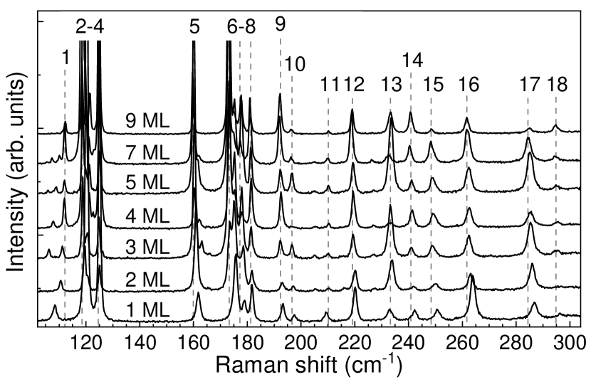
The RS spectra in higher energy range measured on flakes with thicknesses ranging from 1 ML to 9 MLs ReSe2 are presented in Fig. 4. The in-plane ReSe2 anisotropy results in the extremely rich RS spectra, which are in accordance with published reports Wolverson et al. (2014); Zhao et al. (2015); Lorchat, Froehlicher, and Berciaud (2016); Choi et al. (2020). As previously mentioned, there are 18 Raman active peaks, all observed in the frequency range from 100 cm-1 to 300 cm-1. The considerable sensitivity of some Raman peaks intensities to layer thickness should be noted. It is difficult to conduct a thorough analysis of this behavior without taking into account the orientation of each flake, which is crucial considering the anisotropic nature of the ReSe2 crystal Choi et al. (2020). To draw substantive conclusions a comprehensive polarization-resolved measurement should be performed, which stays out of the scope of this work.
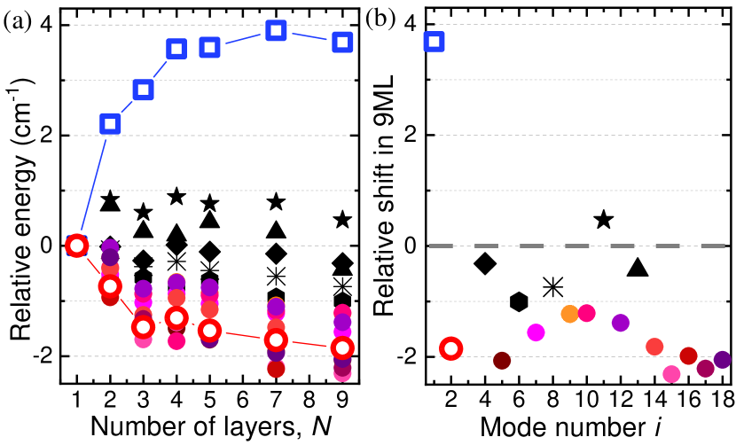
As can be appreciated in Fig. 5(a), the energies of the observed RS modes evolve as a function of the ReSe2 thickness. Basically, three distinct types of dependencies can be noticed. Most of the peaks redshift when the number of layers is increased with the relative energy difference between the 9 ML and 1 ML of 1-2 cm-1 (see Fig. 5(b)). There are a few peaks (4, 6, 8, 11, 13), which do not change substantially their energies in the studied range of thicknesses. Finally, peak 1 experiences a significant blueshift of almost 4 cm-1 between 1 ML and 9 ML. This distinctive evolutions presented in Fig. 5 results from the interplay of interlayer and surface effects Froehlicher et al. (2015); Luo et al. (2013).
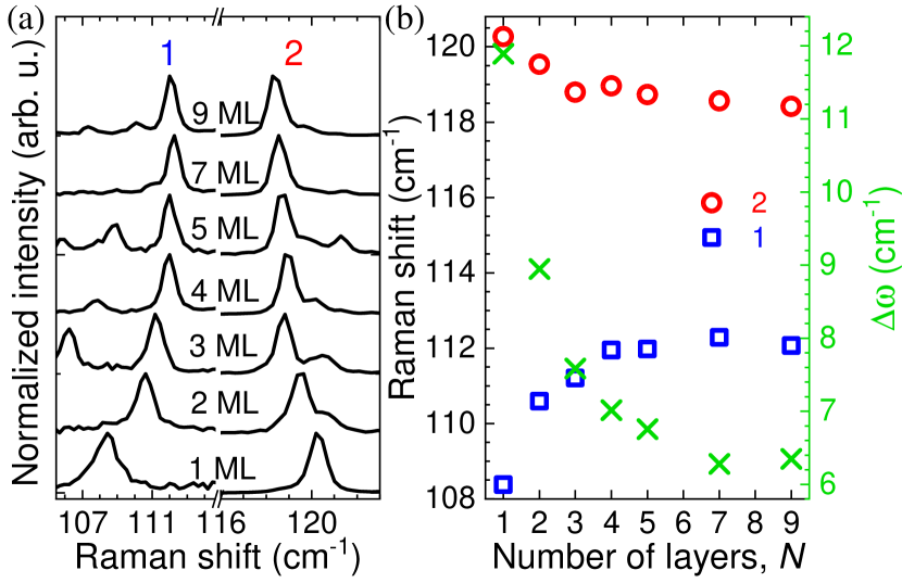
The observed evolution of phonon energies can be very useful to examine the layer’s thickness. Let us focus on the specific part of the spectrum, between 100 cm-1 and 130 cm-1, which is shown in Fig. 6(a). In this range mainly two lines denoted as 1 and 2 can be observed. As already discussed, the phonon mode, labeled 1, blueshifts with an increasing number of layers from 1 ML to 9 MLs, while the peak, labeled 2, displays a redshift. To provide a better illustration of this behavior, we present the extracted energies of both modes for each number of layers in Fig. 6(b). Additionally, the energy difference between peaks 1 and 2 () is demonstrated in Fig. 6(b), which exhibits a distinct evolution as a function of layer thickness. The value of almost 12 cm-1 for a monolayer is reduced by approximately half in the case of 7-9 layers. This dependency provides a simple and reliable means to identify the sample thickness in a few-layer limit.
IV Summary
In conclusion, we have presented the studies of the optical response (photoluminescence and Raman scattering spectra) of a series of ReSe2 structures with thicknesses varying from a monolayer to nine layers. The low-temperature PL spectra of atomically thin ReSe2 flakes comprise two well-resolved emission lines, which experience a blueshift of about 120 meV when the layer thickness is decreased from 9 MLs to a monolayer limit. The energy of those peaks can be used to determine the layer thickness, but this approach is effectively limited, especially due to the low-temperature conditions of the measurement. The analysis of low-energy interlayer Raman modes allows unambiguous identification of the structure thickness in thin layers of S-TMDs. However, demanding experimental conditions, which enable to approach the excitation laser line as close as 5 cm-1, hardly provide a simple characterization tool of S-TMDs. The most convenient way to determine the flake thickness in thin layers of ReSe2 relies on the energy difference between two phonon modes of intralayer vibrations observed at 120 cm-1. The energy difference between the peaks changes from 12 cm-1 to almost 6 cm-1 between 1 ML and 9 MLs. This observation seems to be applicable for other Re-based compounds, ReS2.
Acknowledgements
The work has been supported by the the National Science Centre, Poland (grants no. 2017/27/B/ST3/00205, 2017/27/N/ST3/01612 and 2018/31/B/ST3/02111).
Data availability
The data that support the findings of this study are available from the corresponding author upon reasonable request.
The following article has been accepted by Journal of Applied Physics. After it is published, it will be found at https://dx.doi.org/10.1063/5.0015289.
References
References
- Koperski et al. (2017) M. Koperski, M. R. Molas, A. Arora, K. Nogajewski, A. O. Slobodeniuk, C. Faugeras, and M. Potemski, “Optical properties of atomically thin transition metal dichalcogenides: observations and puzzles,” Nanophotonics 6, 1289 (2017).
- Wang et al. (2018) G. Wang, A. Chernikov, M. M. Glazov, T. F. Heinz, X. Marie, T. Amand, and B. Urbaszek, “Colloquium: Excitons in atomically thin transition metal dichalcogenides,” Rev. Mod. Phys. 90, 021001 (2018).
- Jariwala, Thamizhavel, and Bhattacharya (2017) B. Jariwala, A. Thamizhavel, and A. Bhattacharya, “ReSe2: a reassessment of crystal structure and thermal analysis,” J. Phys. D: Appl. Phys. 50, 044001 (2017).
- Lamfers et al. (1996) H.-J. Lamfers, A. Meetsma, G. Wiegers, and J. de Boer, “The crystal structure of some rhenium and technetium dichalcogenides,” Journal of Alloys and Compounds 241, 34–39 (1996).
- Pradhan et al. (2018) N. R. Pradhan, C. Garcia, B. Isenberg, D. Rhodes, S. Feng, S. Memaran, Y. Xin, A. McCreary, A. R. H. Walker, A. Raeliarijaona, H. Terrones, M. Terrones, S. McGill, and L. Balicas, “Phase Modulators Based on High Mobility Ambipolar ReSe2 Field-Effect Transistors,” Scientific Reports 8, 12745 (2018).
- Yang et al. (2014a) S. Yang, S. Tongay, Y. Li, Q. Yue, J.-B. Xia, S.-S. Li, J. Li, and S.-H. Wei, “Layer-dependent electrical and optoelectronic responses of rese2 nanosheet transistors,” Nanoscale 6, 7226 (2014a).
- Corbet et al. (2016) C. M. Corbet, S. S. Sonde, E. Tutuc, and S. K. Banerjee, “Improved contact resistance in rese2 thin film field-effect transistors,” Appl. Phys. Lett 108, 162104 (2016).
- Yang et al. (2014b) S. Yang, S. Tongay, Q. Yue, Y. Li, B. Li, and F. Lu, “High-Performance Few-layer Mo-doped ReSe2 Nanosheet Photodetectors,” Scientific Reports 4, 5442 (2014b).
- Zhang et al. (2016) E. Zhang, P. Wang, Z. Li, H. Wang, C. Song, C. Huang, Z.-G. Chen, L. Yang, K. Zhang, S. Lu, W. Wang, S. Liu, H. Fang, X. Zhou, H. Yan, J. Zou, X. Wan, P. Zhou, W. Hu, and F. Xiu, “Tunable Ambipolar Polarization-Sensitive Photodetectors Based on High-Anisotropy ReSe2 Nanosheets,” ACS Nano 10, 8067–8077 (2016).
- Cho et al. (2017) A.-J. Cho, S. D. Namgung, H. Kim, and J.-Y. Kwon, “Electric and photovoltaic characteristics of a multi-layer res2/rese2 heterostructure,” APL Materials 5, 076101 (2017).
- Lee et al. (2010) C. Lee, H. Yan, L. E. Brus, T. F. Heinz, J. Hone, and S. Ryu, “Anomalous lattice vibrations of single- and few-layer mos2,” ACS Nano 4, 2695 (2010).
- Gehlmann et al. (2017) M. Gehlmann, I. Aguilera, G. Bihlmayer, S. Nemsak, P. Nagler, P. Gospodaric, G. Zamborlini, M. Eschbach, V. Feyer, F. Kronast, et al., “Direct observation of the band gap transition in atomically thin res2,” Nano letters 17, 5187–5192 (2017).
- Aslan et al. (2016) O. B. Aslan, D. A. Chenet, A. M. Van Der Zande, J. C. Hone, and T. F. Heinz, “Linearly polarized excitons in single-and few-layer res2 crystals,” Acs Photonics 3, 96–101 (2016).
- Hart et al. (2017) L. S. Hart, J. L. Webb, S. Dale, S. J. Bending, M. Mucha-Kruczynski, D. Wolverson, C. Chen, J. Avila, and M. C. Asensio, “Electronic bandstructure and van der waals coupling of rese2 revealed by high-resolution angle-resolved photoemission spectroscopy,” Scientific reports 7, 1–9 (2017).
- Arora et al. (2017) A. Arora, J. Noky, M. Drüppel, B. Jariwala, T. Deilmann, R. Schneider, R. Schmidt, O. Del Pozo-Zamudio, T. Stiehm, A. Bhattacharya, P. Krüger, S. Michaelis de Vasconcellos, M. Rohlfing, and R. Bratschitsch, “Highly anisotropic in-plane excitons in atomically thin and bulklike 1t’-rese2,” Nano Letters 17, 3202 (2017).
- Chen et al. (2015) S.-Y. Chen, C. Zheng, M. S. Fuhrer, and J. Yan, “Helicity-resolved raman scattering of mos2, mose2, ws2, and wse2 atomic layers,” Nano Letters 15, 2526 (2015).
- Lorchat, Froehlicher, and Berciaud (2016) E. Lorchat, G. Froehlicher, and S. Berciaud, “Splitting of Interlayer Shear MOdes and Photon Energy Dependent Anisotropic Raman Response in N-Layer ReSe2 and ReS2,” ACS Nano 10, 2752 (2016).
- Grzeszczyk et al. (2016) M. Grzeszczyk, K. Gołasa, M. Zinkiewicz, K. Nogajewski, M. R. Molas, M. Potemski, A. Wysmołek, and A. Babiński, “Raman scattering of few-layers mote2,” 2D Materials 3, 025010 (2016).
- Froehlicher et al. (2018) G. Froehlicher, E. Lorchat, O. Zill, M. Romeo, and S. Berciaud, “Rigid-layer raman-active modes in n-layer transition metal dichalcogenides: interlayer force constants and hyperspectral raman imaging,” J. Raman Spectrosc. 49, 91 (2018).
- Chenet et al. (2015) D. A. Chenet, O. B. Aslan, P. Y. Huang, C. Fan, A. M. van der Zande, T. F. Heinz, and J. C. Hone, “In-plane anisotropy in mono- and few-layer res2 probed by raman spectroscopy and scanning transmission electron microscopy,” Nano Letters 15, 5667 (2015).
- Castellanos-Gomez et al. (2014) A. Castellanos-Gomez, M. Buscema, R. Molenaar, V. Singh, L. Janssen, H. S. J. van der Zant, and G. A. Steele, “Deterministic transfer of two-dimensional materials by all-dry viscoelastic stamping,” 2D Materials 1, 011002 (2014).
- Tongay et al. (2014) S. Tongay, H. Sahin, C. Ko, A. Luce, W. Fan, K. Liu, J. Zhou, Y.-S. Huang, C.-H. Ho, J. Yan, et al., “Monolayer behaviour in bulk res2 due to electronic and vibrational decoupling,” Nature communications 5, 1–6 (2014).
- Ho and Liu (2019) C.-H. Ho and Z.-Z. Liu, “Complete-series excitonic dipole emissions in few layer res2 and rese2 observed by polarized photoluminescence spectroscopy,” Nano Energy 56, 641 (2019).
- Jadczak et al. (2019) J. Jadczak, J. Kutrowska-Girzycka, T. Smolenski, P. Kossacki, Y. S. Huang, and L. Bryja, “Exciton binding energy and hydrogenic rydberg series in layered res2,” Scientific Reports 9, 1578 (2019).
- Choi et al. (2020) Y. Choi, K. Kim, S. Y. Lim, J. Kim, J. M. Park, Z. L. Jung Hwa Kim, and H. Cheong, “Complete determination of the crystallographic orientation of rex2 (x = s, se) by polarized raman spectroscopy,” Nanoscale Horiz. 5, 308 (2020).
- Lin and Tan (2019) M.-L. Lin and P.-H. Tan, “Ultralow-frequency Raman spectroscopy of two-dimensional materials,” in Raman Spectroscopy of Two-Dimensional Materials (Springer, 2019) pp. 203–230.
- Wolverson et al. (2014) D. Wolverson, S. Crampin, A. S. Kazemi, A. Ilie, and S. J. Bending, “Raman Spectra of Monolayer, Few-Layer, and Bulk ReSe2: An Anisotropic Layered Semiconducto,” ACS Nano 8, 11154–11164 (2014).
- Zhao et al. (2015) H. Zhao, J. Wu, H. Zhong, Q. Guo, X. Wang, F. Xia, L. Yang, P. H. Tan, and H. Wang, “Interlayer interactions in anisotropic atomically thin rhenium diselenide,” Nano Research 8, 3651 (2015).
- Froehlicher et al. (2015) G. Froehlicher, E. Lorchat, F. Fernique, C. Joshi, A. Molina-Sánchez, L. Wirtz, and S. Berciaud, “Unified description of the optical phonon modes in n-layer mote2,” Nano Letters 15, 6481–6489 (2015).
- Luo et al. (2013) X. Luo, Y. Zhao, J. Zhang, Q. Xiong, and S. Y. Quek, “Anomalous frequency trends in mos2 thin films attributed to surface effects,” Phys. Rev. B 88, 075320 (2013).