IEEEexample:BSTcontrol
CLR-DRAM: A Low-Cost DRAM Architecture
Enabling Dynamic Capacity-Latency Trade-Off
Abstract
DRAM is the prevalent main memory technology, but its long access latency can limit the performance of many workloads. Although prior works provide DRAM designs that reduce DRAM access latency, their reduced storage capacities hinder the performance of workloads that need large memory capacity. Because the capacity-latency trade-off is fixed at design time, previous works cannot achieve maximum performance under very different and dynamic workload demands.
This paper proposes Capacity-Latency-Reconfigurable DRAM (CLR-DRAM), a new DRAM architecture that enables dynamic capacity-latency trade-off at low cost. CLR-DRAM allows dynamic reconfiguration of any DRAM row to switch between two operating modes: 1) max-capacity mode, where every DRAM cell operates individually to achieve approximately the same storage density as a density-optimized commodity DRAM chip and 2) high-performance mode, where two adjacent DRAM cells in a DRAM row and their sense amplifiers are coupled to operate as a single low-latency logical cell driven by a single logical sense amplifier.
We implement CLR-DRAM by adding isolation transistors in each DRAM subarray. Our evaluations show that CLR-DRAM can improve system performance and DRAM energy consumption by 18.6% and 29.7% on average with four-core multiprogrammed workloads. We believe that CLR-DRAM opens new research directions for a system to adapt to the diverse and dynamically changing memory capacity and access latency demands of workloads.
1 Introduction
DRAM is the prevalent technology for architecting main memory in modern computing systems. During the past two decades, the storage capacity of a commodity DRAM chip has increased by more than two orders of magnitude (e.g., from 128 Mb [87] to 16 Gb [88]) to meet the increasing main memory capacity demands of modern applications. In contrast, DRAM access latency111Commonly measured by tRC (Row Cycle time) [87, 88]. has reduced by only 16.7% over the same period [55, 9, 10, 4, 27, 59, 57, 8]. Modern processors spend hundreds of clock cycles to access data stored in DRAM, which leads to a significant system-level performance bottleneck [98, 70, 28, 111, 112, 71, 72, 40, 5, 73, 52, 2, 39, 65, 20].
The long access latency is not intrinsic to the DRAM technology itself; there is a fundamental trade-off between access latency and storage density in DRAM. For example, vendors optimize commodity DRAM devices for high storage density at the cost of long access latency. In contrast, vendors also offer special-purpose DRAM devices optimized for low latency but with significantly lower storage density compared to commodity DRAM [68, 89]. Recent works attempt to provide the best of both density- and latency-optimized DRAM by developing heterogeneous DRAM architectures [13, 55, 7, 98] that provide low-latency access in a small and fixed region within a DRAM chip. Unfortunately, all of these works make the capacity-latency trade-off statically at design time: the amount of density-optimized or latency-optimized DRAM is fixed once the chip is fabricated.
We observe that existing DRAM architectures that make the DRAM capacity-latency trade-off decision statically at design-time [23, 35, 68, 89, 55, 53, 103, 102, 13] cannot adapt to changes in a system’s main memory capacity and latency demands, which vary over time with workload behavior. Therefore, existing systems miss opportunities to improve performance. For example, commodity density-optimized DRAM is unable to reduce DRAM access latency when applications exhibit low memory capacity demand. Similarly, latency-optimized DRAM cannot extend its memory capacity when memory capacity is insufficient and frequent page faults lead to significant performance degradation. Existing heterogeneous DRAM architectures [13, 55, 7, 98] take a step towards providing the best of both density- and latency-optimized DRAM. However, they leave significant potential for improving DRAM access latency untapped because they employ a fixed-size and small low-latency region that does not always provide the best possible operating point within the DRAM capacity-latency trade-off spectrum for all workloads.
Our goal is to design a low-cost DRAM architecture that can be dynamically configured to have high capacity or low latency at a fine granularity (i.e., at the granularity of a row). To this end, we propose CLR-DRAM (Capacity-Latency Reconfigurable DRAM), which extends the conventional density-optimized open-bitline DRAM architecture (Figure 1a) by adding isolation transistors along the bitlines in each DRAM subarray (Figures 1b and 1c). CLR-DRAM is able to dynamically control how DRAM cells are connected with their corresponding sense amplifiers at the granularity of a DRAM row. The key idea of CLR-DRAM is to enable the ability to dynamically reconfigure any single DRAM row to operate in either max-capacity mode (Figure 1b) or high-performance mode (Figure 1c).
The max-capacity mode (Figure 1b) operates exactly the same as in the conventional open-bitline architecture (Figure 1a) by enabling a subset of the newly-added isolation transistors (shown in green) to mimic the conventional design’s interconnect. Doing so achieves the same storage capacity as an unmodified capacity-optimized DRAM chip. The high-performance mode (Figure 1c) couples every two adjacent physical DRAM cells in the same row along with their two sense amplifiers to operate together as a single low-latency logical cell and a single, but stronger, logical sense amplifier by enabling all of the newly-added isolation transistors.
The two coupled physical cells (e.g., A and in Figure 1c) store the same bit of data encoded using opposite charge levels. The coupled cells connect to both ports (bitline and ) of a sense amplifier, taking advantage of the differential operation principle of the sense amplifier to begin its sensing process much earlier than in the max-capacity mode (and the conventional open-bitline architecture).
The two coupled sense amplifiers (e.g., SA1 and SA2 in Figure 1c) accelerate a DRAM access in three ways. First, they drive the logical cell formed by the two coupled cells simultaneously from both ends of the bitlines, reducing the latency of a DRAM row activation. Second, coupling the two sense amplifiers makes their precharge units operate together to reduce the latency of precharge operations, which prepare the DRAM bank for activating a new row. Third, since refreshing a DRAM row is analogous to performing an activation and precharge on the row [106, 63, 74, 81, 11], a row operating in high-performance mode is refreshed with low refresh latency, which reduces the performance and energy-consumption overheads of DRAM refresh.
We enable two optimizations for DRAM rows operating in high-performance mode, where every two coupled cells store opposite levels of charge. First, we leverage the observation that a cell storing a low level of charge can safely terminate the trailing charge-restoration phase of a DRAM row activation earlier than a cell storing a high level of charge. Doing so reduces the DRAM row charge-restoration latency (tRAS) in high-performance mode even further, thereby improving performance. Second, we exploit the high effective capacitance of the two coupled cells storing opposite charge levels to extend the interval between consecutive refresh operations for a row operating in high-performance mode.
Our detailed circuit-level simulations show that, with all our optimizations enabled, CLR-DRAM significantly reduces DRAM access latency with low overheads. CLR-DRAM allows reducing the activation latency (tRCD) by 60.1%, restoration latency (tRAS) by 64.2%, write recovery latency (tWR) by 35.2%, and precharge latency (tRP) by 46.4% while incurring a modest DRAM chip area overhead of at most 3.2%.
Our evaluations using 41 single-core and 90 four-core multiprogrammed workloads show that CLR-DRAM significantly improves performance and energy efficiency. For multi-core workloads, if we map only 25% of the most-accessed memory pages to high-performance rows, CLR-DRAM provides an average performance improvement of 11.9% while reducing average DRAM energy and power consumption by 21.7% and 8.9%, respectively. If we map all memory pages to high-performance rows, the performance gain, DRAM energy savings, and DRAM power reduction further increase to 18.6% (27.5% for memory-intensive workloads), 29.7% and 12.8%, respectively.
We conduct a sensitivity analysis of extending the refresh interval to show that we can safely extend the refresh interval of DRAM rows operating in high-performance mode by up to 3. If all DRAM rows are configured to operate in high-performance mode, CLR-DRAM reduces the energy consumption of DRAM refresh commands by 87.1% while still providing an average performance improvement of 17.8% in multi-core evaluations.
This paper makes the following key contributions:
-
•
We propose CLR-DRAM, the first DRAM architecture that enables a dynamic trade-off between storage capacity and low-latency operation in DRAM at the fine granularity of a single DRAM row with low hardware cost.
-
•
We show that the conventional open-bitline architecture, originally designed for high DRAM storage capacity, can be exploited to enable the coupled operation of two DRAM cells and two sense amplifiers. Such coupling significantly reduces four major DRAM access latencies (tRCD, tRAS, tRP and tWR) as well as DRAM refresh overhead.
-
•
We evaluate CLR-DRAM’s system-level performance, energy, and power consumption to show that it significantly improves all three metrics across both single-core and multi-programmed workloads.
2 DRAM Background
We provide background on DRAM organization and operation for understanding the details of our proposal. We refer the reader to prior studies [26, 21, 22, 51, 95, 48, 114, 27, 55, 93, 10, 9, 11, 7, 54, 59, 57, 52, 60, 62, 63, 92, 94, 34, 58, 16] for a more detailed description of DRAM architecture.
2.1 DRAM Organization
The DRAM-based main memory of a modern computer system is organized hierarchically. A CPU accesses DRAM through a memory controller. The DRAM can be organized in multiple DRAM channels, and the memory controller communicates with each channel using a separate channel bus that allows operating the channel independently from the others. A channel contains multiple DRAM ranks, where each rank shares the channel bus in a time-multiplexed manner. A rank consists of a set of DRAM chips that operate in lock-step. A DRAM chip is partitioned into multiple DRAM banks, which process different DRAM requests simultaneously.
A DRAM bank consists of multiple (typically between 128 to 512) subarrays as illustrated in Figure 2a. A subarray comprises a two-dimensional DRAM cell array, and each column of cells in this array is connected to a sense amplifier (SA). SAs in each subarray are connected to Global IO (GIO) wires via Local IO (LIO) wires. GIO wires transfer a column of data between SAs of the subarrays and the bank-level Global SA.
In Figure 2b, we take a closer look into a DRAM cell and how it is connected to a sense amplifier. A DRAM cell contains a capacitor that stores one bit of information in the form of electrical charge (e.g., charged/discharged capacitor representing logical ‘1’/‘0’ or vice versa) and an access transistor that connects the capacitor to a bitline (or ). Cells in a column share a bitline, which connects them to a sense amplifier (SA) at the end of the bitline. Similarly, cells in a row share a wordline that drives the gate of each cell’s access transistor. To access data stored in a DRAM cell, the wordline is asserted to enable the charge of a cell capacitor to be shared with the corresponding SA via the bitline.
A sense amplifier (SA) is responsible for amplifying the small amount of electrical charge stored in a DRAM cell to an accessible level. A DRAM SA operates based on the difference in the voltage levels of the pair of bitlines (bitline and ) that are connected to the SA. Once a DRAM cell shares its small amount of charge with one of the two bitlines, the SA amplifies this small perturbation across the bitline pair to an accessible voltage level. An SA also includes a precharge unit that resets the SA and the bitline pair to prepare for access to another DRAM row. We explain the details of a DRAM access in Section 2.2. Throughout this paper, we use the term “sense amplifier (SA)” to refer to both the SA and the precharge unit.
Open-bitline Architecture. Due to the large size of an SA, the relative arrangement of SAs and DRAM cells significantly impacts the storage density of a DRAM chip. A common density-optimized bank design is known as the open-bitline Architecture [7, 41], which places SAs on both sides (i.e., top and bottom) of a subarray as we show in Figure 2a. In this architecture, neighboring DRAM cell are connected to SAs placed on different sides of the subarray through a pair of adjacent bitlines. For example, in Figure 2a, DRAM cell A is connected to SA1 at the top of the subarray while its neighboring cell B is connected to SA2 at the bottom of the subarray.
2.2 DRAM Operation
A DRAM access requires three main steps: row activation, column access, and precharge.
Row Activation. To perform read/write operations on data stored in DRAM cells, stored data must first be loaded into the SAs by activating the row to be accessed. As we show in Figure 3, the row activation process is composed of two phases: charge sharing and charge restoration . Prior to row activation, the bitlines are in a precharged state at the reference voltage level (e.g., ). To activate a row, the memory controller issues a row activation command ACT to the DRAM. The first phase of row activation, charge sharing , starts by asserting the wordline of a row, leading to charge sharing between the bitlines and the capacitors of all the cells along the activated row. Charge sharing slightly perturbs the bitlines and causes a small difference in the bitline voltage . During the charge restoration phase , each SA amplifies the small difference in bitline voltage to a level suitable for read/write access. Charge restoration also replenishes the charge in the cell capacitor since, during this phase, the wordline remains asserted, and thus the cell capacitor remains connected to the bitline. The DRAM standard specifies the time interval from the beginning of row activation until the two phases complete as tRAS [38, 54, 48, 55].
Column Access. The memory controller can issue a column access command (i.e., read, write) during the charge-restoration phase once the voltage difference across the bitlines reaches the “ready-to-access” voltage level . The DRAM standard specifies the time interval between the start of row activation and when the bitline reaches the “ready-to-access” voltage level as tRCD [38, 54, 48, 55].
Precharge. To activate a new DRAM row, the memory controller first issues a precharge command (PRE) to precharge the activated row and prepare the bank for a subsequent row activation. The precharge operation de-asserts the wordline to disconnect the activated row of cells from the bitlines and resets the bitlines back to the reference voltage (e.g., ). The DRAM standard specifies the time interval from issuing the precharge command until the precharge completes as tRP [38].
Refresh. A DRAM cell capacitor’s charge leaks over time. To ensure that DRAM retains its data indefinitely, the charge in all cell capacitors in a DRAM chip must be periodically replenished. The memory controller ensures data retention by periodically issuing DRAM refresh commands. The DRAM standard specifies the time interval between two consecutive refresh commands that refresh the same row as the refresh window tREFW. A single refresh command refreshes multiple rows, and the number of refreshed rows depends on the total number of rows in a bank. The DRAM standard further specifies the latency of a refresh command (i.e., time required to complete a single refresh operation) as tRFC [38, 63, 78].
2.3 Sense Amplifier
A DRAM sense amplifier (SA) is connected to a pair of bitlines, and , through its two complementary ports (also denoted as and ). During an access to the DRAM cell, the bitline pair develops from a reference voltage (e.g., ) into complementary voltage levels (e.g., to , ).
Prior to a row activation, the precharge unit in the SA sets the voltage of the bitlines to a reference value and the SA is disabled. Then, the charge sharing phase ( in Figure 3) introduces a small voltage difference () across the bitline pair ( in Figure 3) by letting the cell share its charge with a bitline. In Figure 3, the capacitor of the cell connected to is initially fully charged. Charge sharing then perturbs , making its voltage slightly higher than . After a certain amount of time spent in charge sharing to ensure that reaches a threshold ( ), internal control circuitry enables the SAs. Then, the SA amplifies so that reaches and reaches .
3 CLR-DRAM Architecture
We propose CLR-DRAM, a new DRAM architecture that enhances the conventional open-bitline DRAM architecture with isolation transistors to support dynamic reconfiguration of the connections between DRAM cells and SAs (Section 3.1).
CLR-DRAM enables dynamic reconfiguration of any given DRAM row to operate in either max-capacity mode or high-performance mode (Section 3.2) to better meet varying capacity and performance requirements. CLR-DRAM requires only two control signals (and their complements) per-bank for controlling the isolation transistors across all subarrays of the bank to support row-level reconfigurability between the two modes (Section 3.3).
High-performance mode improves DRAM cell access performance in three ways. First, it reduces three major cell access latency timings: tRCD, tRAS, and tRP (discussed in Section 3.4). Second, it enables early termination of charge sharing to further reduce tRAS and tWR (Section 3.5). Third, it reduces the latency of a refresh operation (tRFC) and increases DRAM cells’ retention times to mitigate performance and energy costs associated with DRAM refresh (Section 3.6).
3.1 Bitline Mode Select Transistors
CLR-DRAM requires small modifications to the state-of-the-art density-optimized open-bitline architecture (Figure 4a). We make two observations about the open-bitline architecture that enable implementing CLR-DRAM at low cost. First, two adjacent DRAM cells in a row (e.g., cells A and B in Figure 4a) are connected to two different SAs (cell A to SA1 and cell B to SA2) at different sides of the subarray (top and bottom). Second, one end of the bitline is connected to the SA of one side of the subarray (marked in red), while the other end of the bitline is close to, but not connected to, the SA on the other side of the subarray (marked in blue).
Leveraging these observations, we implement CLR-DRAM to enable dynamic reconfiguration of the connections between DRAM cells and SAs (Figure 4b) by adding an isolation transistor, called bitline mode select transistor, to each end of every bitline. A Type 1 transistor (colored red) replaces a previous connection between a bitline and a sense amplifier (e.g., between cell A and SA1), and a Type 2 transistor (colored blue) connects a previously unconnected end of a bitline to a sense amplifier (e.g., bitline of cell B to SA1).
3.2 Max-Capacity and High-Performance Modes
CLR-DRAM enables a DRAM row to operate in either max-capacity mode or high-performance mode by reconfiguring the connections between DRAM cells and SAs using the two types of bitline mode select transistors (Type 1 and Type 2). CLR-DRAM can reconfigure such connections when a DRAM row is accessed (i.e., activated). Therefore, the operating mode of a row is independent from that of any other row. Figure 5 shows how Type 1 and Type 2 bitline mode select transistors are configured to operate in max-capacity and high-performance modes, for an example subarray with three rows and four cells per row. A green (faded gray) transistor indicates that the transistor is enabled (disabled).
In max-capacity mode (Figure 5a), CLR-DRAM adopts the open-bitline DRAM architecture’s (Figure 4a) cell-to-SA connections to achieve the same storage capacity as in the baseline open-bitline DRAM architecture. In this mode, CLR-DRAM connects each of the adjacent DRAM cells in a row (e.g., cells A and B in Figure 5a) to a different SA on either side of the subarray (cell A to SA1 and cell B to SA2) to make each DRAM cell operate independently of the other. When accessing a row in max-capacity mode, CLR-DRAM enables Type 1 transistors and disables Type 2 ones in the subarray.
In high-performance mode, CLR-DRAM simultaneously couples each of the 1) adjacent cells in a row (e.g., cell A and in Figure 5b) to operate as a single logical cell with high effective capacitance, and 2) corresponding two SAs (e.g., SA1 and SA2), which drive the coupled cells individually in max-capacity mode, to operate as a single but stronger logical SA driving the logical cell. In this mode, CLR-DRAM reconfigures the connections between DRAM cells and SAs to achieve coupled operation of adjacent cells and their two corresponding SAs in two ways (Figure 5b). First, to couple two adjacent DRAM cells as a logical cell, CLR-DRAM connects both cells to the same SA. For example, cell A is connected to the port of SA1, and cell is connected to the port of SA1. Second, to couple two SAs as a logical SA, CLR-DRAM connects the logical cell to both of the SAs. For example, the logical cell formed by the coupled cells A and is connected to both SA1 on the top and SA2 at the bottom of the subarray. When accessing a row in high-performance mode, CLR-DRAM enables both Type 1 and Type 2 transistors in the subarray.
Although this coupled operation of adjacent DRAM cells and their two sense amplifiers sacrifices half of a row’s total storage capacity, it improves DRAM cell access performance in three ways. First, it significantly reduces cell access latency by increasing the total effective cell capacitance and strengthening the overall sense-amplification capabilities (Section 3.4). Second, it enables early-termination of the charge restoration process to further reduce the row activation latency by exploiting the difference in charge restoration speed between the coupled discharged and charged cells (Section 3.5). Third, it reduces the cost of refresh operations by enabling a lower refresh latency and a longer retention time (Section 3.6).
3.3 Control of Bitline Mode Select Transistors
To reconfigure the connections between DRAM cells and SAs within a subarray as described in Section 3.2 for max-capacity and high-performance operation, we introduce two control signals, ISO1 and ISO2, to control the Type 1 and Type 2 bitline mode select transistors in the subarray, respectively. For example, asserting ISO1 and deasserting ISO2 configures a row to operate in max-capacity mode, and asserting both ISO1 and ISO2 configures a row to operate in high-performance mode.
At the same time, the control circuitry of CLR-DRAM must properly configure the bitline-SA connections in the two neighboring subarrays to: 1) ensure correct operation of the SAs in max-capacity mode by connecting certain bitlines in the adjacent subarrays to the SAs as in the conventional open-bitline architecture (Figure 4a), and 2) maximize the latency reduction in high-performance mode by disconnecting all bitlines in the neighboring subarrays from the SAs to avoid increasing the effective bitline length (and hence the capacitance seen by the SAs).
To satisfy the aforementioned requirements without introducing extra control signals, CLR-DRAM alternates between applying two sets of control signal assignments {, } and { , } to odd and even numbered subarrays, respectively.
Figure 6 illustrates CLR-DRAM’s operation in max-capacity and high-performance modes with the previously-mentioned alternating control signal assignments across adjacent subarrays. We simplify our explanations by depicting only one row consisting of two adjacent DRAM cells in each subarray. Enabled transistors are marked in green.
To configure a row in either an odd-numbered or even-numbered subarray to operate in max-capacity mode, CLR-DRAM asserts ISO1 and deasserts ISO2 (Figure 6a). Doing so configures the connections between DRAM cells and SAs to be equivalent to the conventional Open-Bitline DRAM architecture, where cells and SAs operate individually.
To configure a row in an odd-numbered subarray (e.g., Subarray 1 in Figure 6b) to operate in high-performance mode, CLR-DRAM asserts both ISO1 and ISO2. For an even-numbered subarray (e.g., Subarray 0 or Subarray 2 in Figure 6c), CLR-DRAM deasserts both ISO1 and ISO2. In both cases, all bitline mode select transistors in the subarray are enabled to couple every two adjacent DRAM cells and their two SAs in the row to operate as a single logical cell driven by a single logical SA. By assigning the complements of the control signals to neighboring subarrays, all bitlines in neighboring subarrays are disconnected to prevent them from degrading the latency reduction benefits in high-performance mode.
3.4 Reducing Access Latency in High-Perf. Mode
Operating in high-performance mode changes how the cells and the sense amplifiers are connected to achieve two kinds of coupled operation at the same time. First, high-performance mode couples every two adjacent physical DRAM cells in a row to simultaneously operate as a single logical cell. It does so by connecting the two cells to both the bitline and ports of a sense amplifier. Second, high-performance mode couples two sense amplifiers to operate as a single logical sense amplifier driving the single logical cell. CLR-DRAM reduces access latency because the single logical cell is simultaneously connected to two sense amplifiers, which originally served the two cells individually (i.e., in the baseline architecture or in max-capacity mode), on both sides of a subarray. The two coupled sense amplifiers drive the single logical cell from both ends of the same pair of bitlines.
To illustrate the detailed behavior of high-performance mode, Figure 7 shows our SPICE simulation of the change in voltage level on the pair of bitlines (bitline and ) and the two coupled cells (cell and ) during row activation and precharge in CLR-DRAM’s high-performance mode (bottom), and the baseline open-bitline architecture (top). We make three observations.
First, two coupled cells always store opposite charge levels (i.e., charged and discharged) to represent the same logical bit (cell and in Figure 7 (bottom)), because the sense amplifiers always drive bitline and to complementary voltage levels.
Second, two coupled cells with opposite charge levels drive their respective bitlines in opposite directions during the initial charge sharing phase of a row activation . This creates a larger across bitline and relative to the baseline architecture, where only one cell drives either bitline or , but not both. Because a sense amplifier enters the charge-restoration phase when reaches the threshold level , a larger causes the threshold level to be reached more quickly. By shortening the charge sharing phase, we reduce DRAM timing parameters that depend on the charge sharing latency (i.e., tRCD and tRAS ).
Third, the reduction in tRCD and tRAS is larger than the reduction in the charge sharing time. This is because coupling two sense amplifiers to drive the two coupled cells simultaneously from both ends of the bitline pair fundamentally accelerates the entire row activation process. As explained in Section 2.1, coupling two sense amplifiers also couples the two precharge units associated with each of them, thereby also reducing the precharge latency (tRP ).
3.5 Early-Termination of Charge Restoration
CLR-DRAM reduces the latency of DRAM operations involving charge restoration (e.g., tRAS of row activations) for high-performance mode rows even further (on top of reductions shown in Section 3.4) by exploiting three observations on the charge restoration process of coupled cells.
First, the two coupled cells storing opposite levels of charge have higher effective capacitance compared to a single cell. This allows the cell to tolerate more charge leakage while still maintaining the target retention time (e.g., 64ms).
Second, the charge restoration phase has a long tail latency. As shown in our example SPICE simulation of a row activation (Figure 8), about half of the charge restoration phase is spent on restoring the last 25% of charge to the charged cell. In other words, terminating the charge restoration process before the cell is fully restored to does not significantly degrade the charge level in the cell.
Third, the charge restoration speed of a discharged cell is fundamentally faster than that of a charged cell (Figure 8 ). The reason for this difference is similar to that of the difference in charge-sharing speed between charged and discharged cells [41], resulting in asymmetric charge restoration currents for charged and discharged cell capacitors. This means that we can terminate charge restoration before the charged cell is fully restored but after the discharged cell is, and still reduce the charge sharing time.
Leveraging the three aforementioned observations, we terminate the charge restoration phase of the row activation early when the charged cell in the two coupled cells reaches (early termination voltage level), a level smaller than the conventional full-restoration level (), to further reduce tRAS (Figure 8 ). We set to be small enough to provide a non-trivial reduction of tRAS while ensuring that the following two requirements are met. First, the coupled cell must still meet the target retention time (e.g., 64 ms) when charge restoration is terminated early. Second, should not be so small that it significantly degrades the amount of charge available for the next row activation, which could in turn require increasing tRCD. Our analysis (Section 7.2) shows that early termination applies to both row activation and write restoration, whose charge restoration phases are analogous to each other. By terminating charge restoration early for both operations, we reduce tRAS and tWR significantly (by more than 30%) on top of the tRAS reductions provided by techniques described in Section 3.4, while only marginally increasing tRCD (by less than 2%) due to reduction in the amount of charge available for the next activation.
3.6 Mitigating Refresh Costs
CLR-DRAM mitigates the performance and energy overheads of refresh in two ways: 1) reducing refresh latency and 2) reducing refresh rate.
Reducing Refresh Latency. Since a refresh operation is essentially an activation followed by a precharge, whose latencies are both reduced in CLR-DRAM’s high-performance mode, CLR-DRAM also reduces the latency of a refresh operation (i.e., refresh cycle time, tRFC) for a row operating in high-performance mode.
Reducing Refresh Rate. The logical cell formed by coupling two adjacent DRAM cells has a larger capacitance compared to a single DRAM cell. In other words, a logical cell can tolerate more leakage than a single DRAM cell without affecting the integrity of the data stored in it, which increases its retention time and thus allows reducing the refresh rate (i.e., increasing the refresh window tREFW).
Extending tREFW limits how much CLR-DRAM can reduce the row activation latency (tRCD and tRAS) in high-performance mode. A larger tREFW essentially reduces the charge level of the logical cell prior to activation, requiring a longer charge sharing phase for the SA to correctly sense the stored data. Section 7.3 provides a sensitivity analysis quantifying the trade-off between the refresh window (tREFW) and the row activation latency (tRCD and tRAS) in high-performance mode.
4 CLR-DRAM Column Access
We design CLR-DRAM’s column I/O circuitry to maintain full column access bandwidth between the SAs and the global I/O circuitry in both max-capacity and high-performance modes. To do so, we add a single isolation transistor, called column I/O mode select transistor, for each pair of SAs. It enables CLR-DRAM to connect only one of two coupled SAs to the global I/O circuitry in high-performance mode to avoid transferring duplicated data values from the coupled SAs.
Conventional Column Access. Figure 9a illustrates a simplified conventional column I/O architecture, in which a row contains only two columns, and each column contains two cells (e.g., cells A and B form the blue column, cells C and D form the red column). The I/O circuitry is responsible for communicating a column of data (e.g., bits in cell A and B) from a subarray’s local SAs (e.g., SA0 and SA1) to the bank-level global SAs (e.g., GSA[0:1]) via local I/O (e.g., LIO0 and LIO1) and global I/O (e.g., GIO0 and GIO1) lines. Column-select signals (e.g., CSEL0 and CSEL1) control column select transistors to ensure that at most one column in a subarray is connected to LIO lines at a given time. Similarly, GIO lines are time-multiplexed across subarrays in a bank.
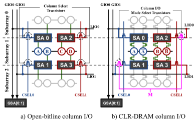
CLR-DRAM Column Access. Since CLR-DRAM’s high performance mode couples two sense amplifiers of two adjacent cells (e.g., SA0 and SA1 in Figure 9b) as one logical sense amplifier, employing the conventional column I/O architecture would waste half of the available LIO and GIO lines to transfer redundant bits (e.g., both SA0 and SA1 contain data “A”). To fully utilize the available column I/O bandwidth (as in the conventional subarray architecture and max-capacity mode), CLR-DRAM adds an isolation transistor, called the column I/O mode select transistor, for each pair of physical sense amplifiers (as shown in Figure 9b). We use a column I/O mode select signal M that controls all column I/O mode select transistors in a subarray. In max-capacity mode, M is asserted so that the subarray I/O operates in a way equivalent to the conventional subarray I/O. In high-performance mode, M is deasserted to disconnect the different redundant halves of the columns (e.g., SA1 in the blue column and SA2 in the red column) from the I/O circuitry, while asserting two column select signals (e.g., CSEL0 and CSEL1) to utilize all of the available data bandwidth. For example, CLR-DRAM can simultaneously access two different bits in SA0 and SA3 in Figure 9b in high-performance mode.
5 System Integration
CLR-DRAM enables a dynamic system-level trade-off between DRAM capacity and DRAM latency adjustable at the granularity of a DRAM row. The system is free to expose this trade-off to any level of the system stack. However, there are two challenges that may complicate communication between CLR-DRAM and other parts of the system: 1) controlling the data mapping between physical addresses and DRAM rows due to memory controller address mapping policies and 2) DRAM refresh control logic. This section discusses each of these challenges and explores potential solutions.
5.1 Memory Controller Address Mapping
The memory controller typically applies an address interleaving policy that distributes memory accesses throughout different levels of the DRAM hierarchy (i.e., channels, ranks, banks) to improve memory access performance by exploiting parallelism in DRAM [79, 90, 1, 32, 33, 49, 100, 51, 83]. The address interleaving policy can potentially split up a single physical page so that different parts of the page are mapped to different DRAM rows. Therefore, multiple DRAM rows may have to be configured to operate in high-performance mode when software requests the allocation of a single low-latency memory page through the OS. As a consequence, because each DRAM row may contain parts of multiple different physical pages, all of the physical memory pages that the newly-configured high-performance rows collectively contain also become low-latency pages. Thus, the address interleaving policy can increase the granularity at which the system interfaces with CLR-DRAM.
Figure 10 provides an example address interleaving scheme and shows how the memory controller might map physical addresses to different levels of the DRAM hierarchy. The memory controller generates the DRAM column address using the bits marked , taken from the page number field of the physical address, but not the bits marked , taken from the page offset field of the physical address. Thus, for a given physical address, bits indicate how many other pages are also mapped to the same DRAM row and bits indicate how many different DRAM rows the page is striped across.
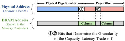
For example, if has bits and has bits, when the system specifies that a page should have low latency, a total of pages222High-performance rows provide half of the total row capacity, so we multiply the result by . will become low-latency pages (since the entirety of the row will be in high-performance mode), causing rows in CLR-DRAM to switch to high-performance mode.
To best take advantage of such a coarse reconfiguration granularity, we believe that the system should “gang together” multiple pages that would benefit from being mapped to a high performance row and map them together. We believe such information about multiple pages can be communicated from the software to hardware via changes to the system software and can be done more easily by adopting new frameworks such as VBI [24], Labeled RISC-V [113], PARD [67], and XMem [107]. We leave the exploration of the (system) software stack for CLR-DRAM to future work.
5.2 Supporting Heterogeneity in Refresh
High-performance mode rows in CLR-DRAM introduce heterogeneity in DRAM refresh operations in two ways. First, compared to rows operating in max-capacity mode, the latency of a refresh operation (tRFC) is reduced due to the faster row activation and precharge. Second, the time interval between two consecutive refresh operations to a high-performance row (tREFW) can be extended compared to a max-capacity row. Such heterogeneity requires the refresh control logic to be able to distinguish between rows operating in max-capacity mode and high-performance mode to 1) apply different tRFC timing constraints, and 2) issue refresh commands at different rates.
6 Capacity and Hardware Overhead Analysis
We analyze the capacity and hardware (Sections 6.1 and 6.2) overheads that CLR-DRAM introduces, including changes to the subarray, the subarray column I/O circuitry, and the memory controller.
6.1 DRAM Capacity Overhead
Any DRAM row configured to operate in high-performance mode provides half of the storage capacity of a conventional DRAM row. Therefore, configuring % of all rows in a DRAM bank to operate in high-performance mode results in an % reduction in the total DRAM capacity. We argue that this reduction in memory capacity is not a significant downside of CLR-DRAM due to two reasons.
First, CLR-DRAM allows the user or the system to dynamically reconfigure DRAM and find a favorable operating point in the DRAM capacity-performance trade-off space. In edge cases where the system requires more memory capacity (e.g., to avoid frequent page swaps), it can configure more DRAM rows in CLR-DRAM to operate in max-capacity mode.
Second, previous works show that many modern workloads under-utilize the main memory capacity (e.g., in HPC [77], cloud [85, 12], and enterprise [17] domains). In such workloads, the user or system can trade the under-utilized memory capacity to improve system performance by switching more DRAM rows to high performance mode.
We leave it to the user or the system software to determine a suitable balance between the two operating modes. A user cognizant of a workload’s memory usage characteristics can use CLR-DRAM to configure DRAM rows to operate in high-performance or max-capacity mode as needed by the workload. We leave a rigorous exploration of how different workloads and systems can exploit the new dynamic capacity-latency reconfigurability and the associated trade-offs enabled by CLR-DRAM to future work.
6.2 Hardware Overhead
CLR-DRAM requires modest hardware changes to the DRAM chip and memory controller circuitry. This section analyzes the impact of these changes on overall chip area.
DRAM Chip Overhead. CLR-DRAM adds two sets of isolation transistors to a density-optimized DRAM chip: 1) bitline mode select transistors and 2) column I/O mode select transistors. First, two bitline mode select transistors added to each bitline in a subarray (i.e., one at either end of each bitline) enable switching of a row between the two operating modes. This increases the height of a DRAM subarray, resulting in an area overhead of 1.6% of the DRAM chip.333We size the isolation transistors according to prior work [91, 80]. Second, CLR-DRAM adds column I/O mode select transistors next to half of the existing column select transistors to provide the same column I/O data transfer bandwidth in both high-performance and max-capacity modes. While it is possible that the column I/O mode select transistors may fit into existing slack space without increasing the chip area, we conservatively assume that no slack space is available for CLR-DRAM to exploit.444We assume the worst case due to the lack of open literature on modern DRAM I/O circuitry designs that we could use to accurately evaluate whether the mode select transistors can fit into the existing slack area. Assuming that a column I/O mode select transistor requires the same area as a bitline mode select transistor, it incurs an additional 1.6% DRAM chip area overhead. Overall, even with this conservative estimate, CLR-DRAM increases the DRAM chip area by only 3.2%, compared to a commodity density-optimized DRAM baseline.
Memory Controller Overhead. In CLR-DRAM, the memory controller uses two separate sets of timing parameters to access and refresh DRAM rows in max-capacity mode and high-performance mode. To fully utilize the row-level reconfigurability, the memory controller needs to track the operating mode of each DRAM row to apply proper timing parameters. Without optimization, this requires storing one bit per row. However, the required storage reduces by a factor of if the memory controller address mapping requires the reconfiguration granularity of CLR-DRAM to be larger than a single row (discussed in Section 5.1). The required storage may be optimized even further using a more efficient representation. Many space-efficient data structures are commonly used in hardware systems (e.g., sparse bitmaps [39]), and systems integrating CLR-DRAM can potentially make use of similar approaches.
6.3 Handling Row and Column Redundancy
A modern DRAM chip internally remaps known faulty DRAM rows/columns to redundant rows/columns that are provided as spares to handle post-manufacturing faults [30]. Because CLR-DRAM performs reconfiguration at the granularity of a single row, it is fully compatible with existing row redundancy resources. However, our design may use more redundant columns compared to conventional DRAM because, if a faulty column is remapped to a spare column, its adjacent column must also be remapped to the corresponding adjacent spare column in order to ensure that all cells throughout the row can be coupled pairwise for high-performance mode operation. For commodity devices in the field, redundant rows and columns are typically underutilized [46, 76] (e.g., <25% utilization [46]). Therefore, CLR-DRAM likely does not require increasing the amount of available redundant row or column resources to implement the high-performance mode.
7 Circuit Simulations
We use SPICE circuit simulations to evaluate the latency and refresh reductions CLR-DRAM provides.
7.1 Methodology
We use a methodology similar to that of prior work [26]. We model a DRAM subarray in SPICE based on Rambus DRAM technology parameters [82] and scale the technology parameters to 22 nm according to the ITRS roadmap [37, 108]. We have open sourced our SPICE circuit model [86].
-
•
We model the sense amplifier using the 22nm PTM high-performance transistor model [80].
-
•
We model the worst-case operating conditions with a temperature of 85°C.
- •
-
•
We tune other parameters (e.g., bitline capacitance and resistance) to the best of our ability so that the timing parameters derived from our model closely approximate real DDR4 datasheet values [38].
We model manufacturing process variation by running iterations of Monte Carlo simulations with 5% variation in every circuit component. We derive the timing parameters of our design based on the slowest of the iterations and make sure that every single iteration reads the correct value from the the cell.
7.2 Latency Reduction
Table 1 shows the key DRAM timing parameters of conventional DRAM (i.e., our baseline) and the two operating modes of CLR-DRAM. Overall, we observe 35–65% reduction in the four key timing parameters in high-performance mode.
| Timing Parameter | Baseline | Max-Cap. | High-Performance | Reduction | |
| w/o E.T. | w/ E.T. | (w/ E.T.) | |||
| tRCD (ns) | 13.8 | 13.2 | 5.4 | 5.5 | 60.1% |
| tRAS (ns) | 39.4 | 40.3 | 20.3 | 14.1 | 64.2% |
| tRP (ns) | 15.5 | 8.3 | 46.4% | ||
| tWR (ns) | 12.5 | 13.3 | 12.5 | 8.1 | 35.2% |
Impact of Bitline Mode Select Transistors in Max-Capacity Mode. The timing parameters for rows operating in max-capacity mode are different from those of the baseline because of the insertion of the bitline mode select transistors. The bitline mode select transistors impact timing in three ways. First, they slightly reduce tRCD by 4.4% because they decouple the SAs from the long bitlines that have large capacitance. Second, at the same time, they also limit the amount of current that can pass through the bitline, making tRAS and tWR slightly higher than in the baseline (by 2.2% and 6.4%, respectively). Third, they enable CLR-DRAM to reduce the precharge latency tRP by 46.4% regardless of the target row’s operating mode, by coupling two precharge units during the precharge operation (similarly to LISA-LIP [7]). Our evaluations in Section 8.1 show that these three changes in the timing parameters have an overall positive impact on system-level performance.
Early Termination of Charge Restoration. As described in Section 3.5, we reduce tRAS and tWR in high-performance mode by terminating charge restoration early. Table 1 shows the reduction in tRAS and tWR with by applying early termination of charge restoration (w/ E.T. column) compared to without applying it (w/o E.T. column). We find that applying early termination of charge restoration reduces tRAS even further and enables the reduction of tWR555 Compared to the conventional DRAM architecture that uses only one SA per cell, write operations to a high-performance row in CLR-DRAM require a single write driver to drive two coupled SAs. Without terminating charge restoration early, the additional load on the write driver offsets the write latency (tWR) benefits of using coupled cells and SAs in high-performance mode. , while increasing tRCD by only 0.1 ns. The marginal increase in tRCD is because the reduced charge level in the charged cell of the two coupled cells reduces the initial developed across the bitline pair at the very beginning of a row activation, thus extending the length of the charge sharing phase.
7.3 Refresh Interval Versus Latency
Section 3.6 introduces the fundamental trade-off between the extended refresh interval (tREFW) and access latency (tRCD and tRAS). In this section, we analyze the sensitivity of tRCD and tRAS to the increase in the refresh interval.
We perform a sweep of the time interval between consecutive refresh operations to the same row (tREFW) and study how changing tREFW affects tRCD and tRAS (with early-termination of charge restoration applied). We sweep the refresh interval in increments of 10ms until the reduced charge level in the cell prior to activation is too low for the SA to sense correctly. Figure 11 shows the results of our sensitivity analysis. We make two observations.
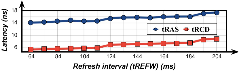
First, we observe that extending the refresh interval increases tRCD and tRAS. This is because extending the refresh interval reduces the charge level in the cell prior to activation, which extends the charge sharing phase. When the refresh interval is extended from 64ms to 194ms (a 3.03 increase), tRCD and tRAS increase by 3.24ns and 3.04ns (by 1.58 and 1.21), respectively.
Second, these increases in tRCD and tRAS are large enough to potentially degrade system-level performance. To study the system-level effect of the trade-off between reducing the refresh rate and increasing tRCD and tRAS, we perform a sensitivity analysis using the timing parameters from Figure 11 in Section 8.5.
8 System-Level Evaluation
We use system-level performance and power simulation to evaluate CLR-DRAM on single- and multi-core systems.
8.1 Methodology
Simulators. We use a customized version of Ramulator [51], a cycle-accurate DRAM simulator, to evaluate CLR-DRAM’s system-level performance. We use Ramulator’s CPU-trace driven simulation mode with application traces generated from a custom Pintool [84, 66]. We use DRAMPower [6] to evaluate the power and energy consumption of CLR-DRAM with the DRAM command traces generated by Ramulator.
System Configuration. The configuration of the system used in our evaluations is shown in Table 2.
| Processor | 1-4 core(s), 4GHz, 4-wide issue, 8 MSHRs per core | ||
|---|---|---|---|
| 128-entry instruction window | |||
| LLC | 64-byte cacheline, 8-way associative, 8MB total capacity | ||
| Memory | FR-FCFS-Cap scheduling policy [71], timeout-based row policy666A row-buffer management policy that closes an open row after 120 ns if there are no outstanding requests to that row., | ||
| Controller | 64-entry read/write request queue | ||
| DRAM |
|
||
| Benchmarks |
|
Workloads. Our evaluation includes 1) 41 real applications from the SPEC CPU2006 [99], TPC [105] and MediaBench [19] benchmark suites and 2) 30 in-house synthetic random and stream access workloads [26, 69, 50]. The random workloads randomly access memory locations, and thus exhibit a very limited row locality. The stream workloads access contiguous memory locations, exhibiting high row locality.
Our single-core evaluation covers all 71 workloads. For multi-core evaluation, we first categorize the 41 real applications as memory-intensive or non-memory-intensive based on the misses-per-kilo-instruction (MPKI) metric from the last-level-cache. MPKI is calculated using the SimPoint [25] traces of the representative phases of each application in single-core simulations. Applications with MPKI are classified as memory-intensive. We form three multi-programmed four-core workload groups, each containing 30 workloads consisting of four randomly-selected single-core applications. The three groups are: 1) Low memory intensity (“L”) that contains four non-memory-intensive applications, 2) Medium memory intensity (“M”) that contains two non-memory-intensive and two memory-intensive applications, and 3) High memory intensity (“H”) that contains four memory-intensive applications. We simulate the multi-core workloads until each CPU core completes at least 200 million instructions. For all configurations, we initially warm up the caches by fast-forwarding 100 million instructions.
Baseline DRAM Timing Parameters. We derive the DRAM timing parameters related to accessing the DRAM cell array (tRCD, tRAS, tRP and tWR) from our SPICE simulations explained in Section 7.2. We obtain the other DRAM timing parameters from the datasheet of a commodity 16Gb DDR4 DRAM chip [88].
CLR-DRAM Parameters. We obtain tRCD, tRAS, tRP and tWR for max-capacity and high-performance rows from our SPICE simulations (Section 7.2). We always apply early termination of charge restoration to reduce tRAS and tWR because early termination is largely beneficial aside from a marginal increase in tRCD. To calculate tRFC for high-performance rows, we reduce the default tRFC by a factor equal to the average reduction in tRAS and tRP.
CLR-DRAM Data Mapping. We model 4 different configurations representing how CLR-DRAM could be configured in a system where 25%, 50%, 75%, 100% of all the DRAM rows are high-performance rows. We use a profiling-based approach (similar to prior works [98, 13]) to assign a workload’s X% of the most frequently-accessed pages to high-performance rows when the system configures X% of all rows to operate in high-performance mode. We evaluate another configuration where all DRAM rows operate in the max-capacity mode (we denote it as 0%).
Metrics. We use the instructions per cycle (IPC) and the weighted speedup [97, 18] metrics to measure the performance of single-core and multi-core systems, respectively. We normalize the IPC, weighted speedup and energy consumption numbers of CLR-DRAM to the baseline DDR4 [38] DRAM to show the performance and energy impact of our design. All average values we present are geometric means.
8.2 Single-core Performance
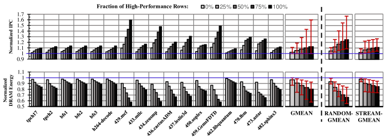
Figure 12 (top) shows CLR-DRAM’s normalized IPC with the five different page mapping configurations (0% to 100%) of memory intensive benchmarks and synthetic (random and stream access) workloads relative to the baseline DRAM. Figure 12 (bottom) shows the DRAM energy consumption of the same CLR-DRAM configurations, normalized to the baseline. The error bars show the maximum/minimum IPC improvement or DRAM energy on each plot. We show detailed results for the 17 benchmarks with the highest MPKI values. GMEAN corresponds to average results across all 41 benchmarks. We make five key observations from these results.
First, CLR-DRAM improves the overall performance of our single-core workloads by 5.5%, 7.9%, 10.3%, and 12.4% when 25%, 50%, 75%, and 100% of the frequent accessed pages are mapped to high-performance mode rows, respectively. No workload experiences slowdown with CLR-DRAM. 429.mcf, with all its pages mapped to high-performance rows, achieves the highest speedup of 59.8%. We conclude that CLR-DRAM significantly improves single-core performance.
Second, CLR-DRAM significantly reduces DRAM energy consumption. By mapping 25%, 50%, 75%, and 100% of the frequently-accessed pages to high-performance rows, CLR-DRAM achieves overall DRAM energy savings of 9.2%, 13.3%, 16.9%, and 19.7%, respectively. The energy savings mainly stem from the reduced execution time of the workloads and reduction in DRAM power consumption (Section 8.4).
Third, different workloads exhibit different sensitivities to reduced DRAM access latency. The results from synthetic workloads clearly show that CLR-DRAM benefits workloads with random access patterns, which frequently experience row buffer conflicts, due to the significant reduction in tRAS and tRP that determine how quickly a row can be opened and closed.
Fourth, different workloads exhibit different scaling behavior as we increase the fraction of frequently-accessed pages mapped to high-performance rows. For example, some workloads (e.g., 429.mcf, 462.libquantum) show near-linear scaling because their memory accesses are distributed relatively evenly across their memory footprint (e.g., the top 25%, 50% and 75% most accessed pages of 462.libquantum cover 26.4%, 51.2% and 75.6% of its memory accesses, respectively). Some others (e.g., 450.soplex, 470.lbm) scale sub-linearly because most of their memory accesses are concentrated in a small fraction of their memory footprint (e.g., 85.2% of 450.soplex’s memory references fall into the top 25% of its most accessed pages). Mapping more pages to high-performance rows provides diminishing speedups in a workload that accesses memory relatively unevenly throughout its memory footprint.
Fifth, operating all rows in max-capacity mode has a small but clearly positive performance impact (an average of 2.4% performance improvement) compared to the baseline DRAM for single-core workloads. This is because coupling two precharge units enables a large reduction in tRP despite the increased tRAS and tWR caused by the bitline mode select transistors. Average DRAM energy consumption is reduced by 3.5%, due to the reduction in tRP. We conclude that, even in the worst case when all rows are configured to operate in max-capacity mode, overall system performance and energy impact of CLR-DRAM is still positive.
Overall, CLR-DRAM significantly improves both the performance and energy consumption of single-core workloads, with increasing benefits as more pages get mapped to high-performance rows.
8.3 Multi-core Performance
Figure 13 shows CLR-DRAM’s weighted speedup (top) and DRAM energy consumption (bottom), both normalized to baseline DDR4 DRAM, across the three workload groups we evaluate in multi-core simulations. We make the following three observations.
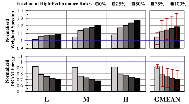
First, CLR-DRAM provides significant overall performance improvement and DRAM energy savings across all 90 multi-core workloads we evaluate. When only 25% of the most-accessed pages are mapped to high-performance rows, CLR-DRAM improves performance by 11.9% on average and DRAM energy consumption by 21.7%. When this fraction is 100%, CLR-DRAM provides an overall performance improvement of 18.6% and DRAM energy savings of 29.7%.
Second, high-MPKI workloads (denoted H in Figure 13) benefit more from reducing the memory access latency in CLR-DRAM’s high-performance mode. When all pages are mapped to high-performance rows, CLR-DRAM provides an average speedup of 27.5% for memory-intensive workloads since memory-intensive workloads are more sensitive to DRAM access latency reduction.
Third, CLR-DRAM provides the smallest DRAM energy reduction for the high-MPKI workloads. One reason for this is that CLR-DRAM reduces tRAS significantly, which can cause a row to close early enough that a request accessing the same row misses in the row buffer when the request is issued shortly after closing the row. This results in more frequent row buffer misses and conflicts, which consume more energy than accesses to an open row, thereby offsetting the energy reduction benefits of the reduced execution time.
We conclude that CLR-DRAM significantly improves performance and energy consumption of multi-core workloads.
8.4 Power Savings of CLR-DRAM
Figures 14a and 14b show the DRAM power consumption of CLR-DRAM normalized to the baseline DDR4 configuration in single-core and multi-core systems, respectively. When 25% of pages are mapped to high-performance DRAM rows, average DRAM power reduces by 4.3% for single-core workloads (8.9% for multi-core workloads). The average DRAM power reduction increases to 9.7% and 12.8% for single- and multi-core workloads, respectively, when the fraction of pages mapped to high-performance rows is 100%. We conclude that CLR-DRAM significantly reduces DRAM power consumption for both single-core and multi-core workloads.
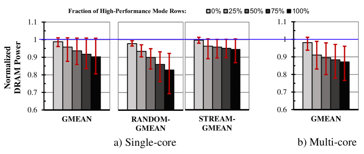
a) single-core and b) multi-core workloads.
8.5 Refresh Interval vs. Access Latency Trade-off
Using two DRAM cells together as a logical cell with larger capacitance compared to the baseline, CLR-DRAM supports extending the default refresh interval (tREFW) for high-performance rows. However, extending tREFW slightly increases tRCD, tRAS, and tRFC (as discussed in Section 3.6), which could potentially have a negative impact on system performance. We evaluate the performance and DRAM energy impact of increasing the refresh interval in CLR-DRAM.
Methodology. We evaluate four representative refresh interval (tREFW) settings: 114 ms, 124 ms, 184 ms, and 194 ms, each with the corresponding tRCD and tRAS values extracted using our SPICE simulations in Section 3.6. We denote these four settings as CLR-114, CLR-124, CLR-184, CLR-194. We perform single-core and multi-core simulations using the same methodology as described in Section 8.1 (we do not evaluate the 0% case as max-capacity mode does not support extending tREFW).
Results. Figures 15a and 15b show the normalized IPC (weighted speedup for multi-core workloads), DRAM energy consumption, and DRAM refresh energy consumption of the four tREFW settings alongside the baseline case of CLR-64 for single- and multi-core workloads. We make the following three observations.
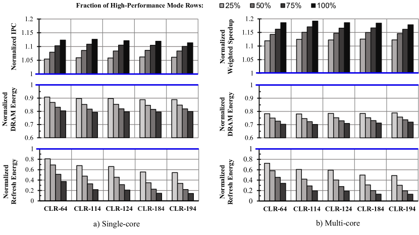
First, extending the refresh interval can either have a slightly positive or negative impact on the system performance depending on by how much the refresh interval increases. For single- and multi-core workloads, CLR-114 provides an average speedup of 12.6% and 19.2% over baseline DDR4, respectively, when all pages are mapped to high-performance rows, outperforming CLR-64 by 0.28% and 0.61%. In contrast, CLR-194 causes an average slowdown of 0.98% and 0.77% compared to CLR-64 (due to longer access latencies), but still outperforms the baseline by 11.4% and 17.8% for single- and multi-core workloads respectively.
Second, the overall DRAM energy consumption of all configurations is similar. This is because the energy spent on DRAM access (not DRAM refresh) is the majority of the total DRAM energy consumption. CLR-114 provides the highest DRAM energy reduction of 29.9% for multi-core workloads.
Third, by reducing tRFC and increasing tREFW, CLR-DRAM saves significant DRAM refresh energy. We observe that CLR-64 without an extended tREFW already reduces refresh energy by 66.1% for multi-core workloads when all DRAM rows operate in high-performance mode because it uses a smaller tRFC. By extending the refresh interval to 194 ms (CLR-194), CLR-DRAM reduces DRAM refresh energy by 87.1%.
We conclude that extending the refresh interval (tREFW) in CLR-DRAM’s high-performance mode effectively reduces the energy overhead of DRAM refresh with negligible performance impact.
9 Related Work
To our knowledge, this is the first work to provide a DRAM architecture that enables dynamic reconfiguration of any row to provide either high storage capacity or low access latency at low hardware cost. CLR-DRAM provides this new dynamic capability using simple modifications to a density-optimized commodity DRAM chip. We briefly discuss related works that exploit static and dynamic DRAM capacity-latency trade-offs, enable in-DRAM caching, reduce access latency, and mitigate refresh costs.
Static Capacity-latency Trade-off. Certain commercial DRAM chips [68, 23, 35] reduce access latency by incorporating small DRAM subarrays and banks. These products statically exploit the capacity-latency trade-off by sacrificing significant storage capacity for reduced latency. CHARM [98] and TL-DRAM [55] statically partition a DRAM chip into a fast region and a slow region. However, the low-latency regions in these designs are small and fixed.
Designs based on Twin-Cell DRAM [102, 103, 53] statically couple every two DRAM cells to reduce access latency and refresh rates. However, Twin-Cell DRAM designs do not couple two sense amplifiers to accelerate the activation and precharge process, which significantly limits their potential to improve DRAM latency compared to CLR-DRAM.
Dynamic Capacity-latency Trade-offs. MCR DRAM [13] simultaneously activates multiple (i.e., two or four) DRAM rows to achieve low row activation latency. This enables a dynamic trade-off between DRAM capacity and performance comparable to our design. However, MCR DRAM does not couple two sets of sense amplifiers and precharge units, which greatly limits the amount of latency reduction it can achieve.
Hsu et al. [31] patent a DRAM array design that provides rows that are interchangeable between single-cell and twin-cell operation. Unfortunately, their design adds a new row of SAs per subarray dedicated to twin-cell operation, which results in high DRAM chip area overhead. Their design also does not couple two SAs, so it has limited potential to reduce DRAM access latency compared to CLR-DRAM.
In-DRAM Caching. SALP [48] utilizes the parallelism between subarrays to enable simultaneously opening multiple DRAM rows in different independent subarrays. CROW [26] enables in-DRAM caching by copying the data of a frequently-accessed DRAM row to another row (i.e., copy-row) in the same subarray. CROW simultaneously activates the two rows that contain the same data to reduce DRAM access latency. To reduce DRAM refresh overhead, CROW eliminates weak rows, which have short retention times, and extends the refresh interval by remapping the weak rows to copy-rows that can retain data for a long time. LISA [7] enables fast data movement across different subarrays in a bank at the granularity of DRAM rows. The LISA-VILLA mechanism utilizes this fast in-bank data movement to cache frequently-accessed data using a small but low-latency subarray within the same bank. Cache DRAM [29] adds a small SRAM cache in a DRAM chip. Because CLR-DRAM enables a new row-granularity capacity-latency trade-off, CLR-DRAM is orthogonal to in-DRAM caching, and mechanisms such as SALP, CROW, LISA, and Cache DRAM can be built on top of the CLR-DRAM architecture to improve performance even further.
Reducing Latency. Various works propose techniques to reliably reduce DRAM latency without sacrificing capacity [54, 115, 27, 9, 59, 47, 110, 10] by reducing timing margins under certain conditions. CLR-DRAM is complementary to mechanisms proposed by these prior works and can be combined with them to reap the benefits of both.
10 Conclusion
We propose CLR-DRAM, new DRAM architecture that enables dynamic fine-grained reconfigurability between high-capacity and low-latency operation. CLR-DRAM can reconfigure every single DRAM row to operate in either max-capacity mode or high-performance mode. A max-capacity row maintains approximately the same storage density as the commodity density-optimized open-bitline architecture by letting each DRAM cell operate separately. A high-performance row provides low access latency and low refresh overhead by coupling every two adjacent DRAM cells in the row and their sense amplifiers. Our evaluations show that CLR-DRAM significantly improves system performance and energy consumption for both single- and multi-core workloads in all our evaluation configurations, including those that favor maximizing capacity and minimizing latency. We hope that future work exploits CLR-DRAM to develop more flexible systems that can adapt to the diverse and dynamically changing DRAM capacity and latency demands of workloads.
Acknowledgments
We thank the anonymous ISCA 2020 reviewers for their feedback and the SAFARI group members for the stimulating intellectual environment they provide. We acknowledge the generous gifts provided by our industrial partners: Alibaba, Facebook, Google, Huawei, Intel, Microsoft, and VMware.
References
- [1] AMD, “BKDG for AMD Family 16h Models 00h-0Fh Processors,” 2013.
- [2] R. Bera et al., “DSPatch: Dual Spatial Pattern Prefetcher,” in MICRO, 2019.
- [3] I. Bhati et al., “Flexible Auto-Refresh: Enabling Scalable and Energy-Efficient DRAM Refresh Reductions,” in ISCA, 2015.
- [4] S. Borkar et al., “The Future of Microprocessors,” in CACM, 2011.
- [5] A. Boroumand et al., “Google Workloads for Consumer Devices: Mitigating Data Movement Bottlenecks,” in ASPLOS, 2018.
- [6] K. Chandrasekar et al., “DRAMPower: Open-source DRAM Power & Energy Estimation Tool,” URL: http://www.es.ele.tue.nl/drampower/, 2012.
- [7] K. K. Chang et al., “Low-Cost Inter-Linked Subarrays (LISA): Enabling Fast Inter-Subarray Data Movement in DRAM,” in HPCA, 2016.
- [8] K. K. Chang, “Understanding and Improving the Latency of DRAM-Based Memory Systems,” Ph.D. dissertation, Carnegie Mellon Univ., 2017.
- [9] K. K. Chang et al., “Understanding Latency Variation in Modern DRAM Chips: Experimental Characterization, Analysis, and Optimization,” SIGMETRICS, 2016.
- [10] K. K. Chang et al., “Understanding Reduced-Voltage Operation in Modern DRAM Devices: Experimental Characterization, Analysis, and Mechanisms,” in SIGMETRICS, 2017.
- [11] K. K.-w. Chang et al., “Improving DRAM Performance by Parallelizing Refreshes with Accesses,” in HPCA, 2014.
- [12] W. Chen et al., “How Does the Workload Look Like in Production Cloud? Analysis and Clustering of Workloads on Alibaba Cluster Trace,” in ICPADS, 2018.
- [13] J. Choi et al., “Multiple Clone Row DRAM: A Low Latency and Area Optimized DRAM,” in ISCA, 2015.
- [14] Z. Cui et al., “DTail: a Flexible Approach to DRAM Refresh Management,” in ICS, 2014.
- [15] A. Das et al., “VRL-DRAM: Improving DRAM Performance via Variable Refresh Latency,” in DAC, 2018.
- [16] R. H. Dennard, “Field-Effect Transistor Memory,” US Patent 3,387,286. 1968.
- [17] S. Di et al., “Characterization and Comparison of Cloud Versus Grid Workloads,” in CLUSTER, 2012.
- [18] S. Eyerman et al., “System-level Performance Metrics for Multiprogram Workloads,” IEEE Micro, 2008.
- [19] J. E. Fritts et al., “Mediabench II Video: Expediting the Next Generation of Video Systems Research,” in Electronic Imaging, 2005.
- [20] S. Ghose et al., “Processing-In-Memory: A Workload-Driven Perspective,” IBM Journal of Research and Development, 2019.
- [21] S. Ghose et al., “Demystifying Complex Workload-DRAM Interactions: An Experimental Study,” SIGMETRICS, 2019.
- [22] S. Ghose et al., “What Your DRAM Power Models Are Not Telling You: Lessons from a Detailed Experimental Study,” SIGMETRICS, 2018.
- [23] GSI, “Low Latency DRAMs,” https://www.gsitechnology.com/lldrams.
- [24] N. Hajinazar et al., “The Virtual Block Interface: A Flexible Alternative to the Conventional Virtual Memory Framework,” in ISCA, 2020.
- [25] G. Hamerly et al., “Simpoint 3.0: Faster and More Flexible Program Phase Analysis,” JILP, 2005.
- [26] H. Hassan et al., “CROW: A Low-Cost Substrate for Improving DRAM Performance, Energy Efficiency, and Reliability,” in ISCA, 2019.
- [27] H. Hassan et al., “ChargeCache: Reducing DRAM Latency by Exploiting Row Access Locality,” in HPCA, 2016.
- [28] J. Hestness et al., “A Comparative Analysis of Microarchitecture Effects on CPU and GPU Memory System Behavior,” IISWC, 2014.
- [29] H. Hidaka et al., “The Cache DRAM Architecture: A DRAM with an On-Chip Cache Memory,” MICRO, 1990.
- [30] M. Horiguchi et al., Nanoscale Memory Repair. Springer SBM, 2011.
- [31] L. L. Hsu et al., “DRAM Array Interchangeable Between Single-cell and Twin-cell Array Operation,” US Patent 6452855B1. 2001.
- [32] Intel Corporation, “The Intel 7300 Chipset Memory Controller Hub (MCH),” https://www.intel.com/content/dam/doc/datasheet/7300-chipset-memory-controller-hub-datasheet.pdf, 2007.
- [33] Intel Corporation, “10th Generation Intel Processor Families Datasheet,” https://www.intel.com/content/dam/www/public/us/en/documents/datasheets/10th-gen-core-families-datasheet-vol-2-datasheet.pdf, 2020.
- [34] E. Ipek et al., “Self-Optimizing Memory Controllers: A Reinforcement Learning Approach,” ISCA, 2008.
- [35] ISSI, “RLDRAM, HPDRAM,” http://www.issi.com/WW/pdf/RLDRAM-flyer_electronica2014.pdf, 2014.
- [36] K. Itoh et al., “Trends in Low-Power RAM Circuit Technologies,” Proc. IEEE, 1995.
- [37] ITRS, “ITRS Reports,” http://www.itrs2.net/itrs-reports.html.
- [38] JEDEC, “DDR4 SDRAM standard, JESD79-4B,” 2012.
- [39] K. Kanellopoulos et al., “SMASH: Co-designing Software Compression and Hardware-Accelerated Indexing for Efficient Sparse Matrix Operations,” in MICRO, 2019.
- [40] S. Kanev et al., “Profiling a Warehouse-scale Computer,” in ISCA, 2015.
- [41] B. Keeth et al., DRAM Circuit Design: Fundamental and High-Speed Topics. John Wiley & Sons, 2007.
- [42] S. Khan et al., “The Efficacy of Error Mitigation Techniques for DRAM Retention Failures: A Comparative Experimental Study,” in SIGMETRICS, 2014.
- [43] S. Khan et al., “PARBOR: An Efficient System-Level Technique to Detect Data-Dependent Failures in DRAM,” in DSN, 2016.
- [44] S. Khan et al., “A Case for Memory Content-Based Detection and Mitigation of Data-Dependent Failures in DRAM,” CAL, 2016.
- [45] S. Khan et al., “Detecting and Mitigating Data-Dependent DRAM Failures by Exploiting Current Memory Content,” in MICRO, 2017.
- [46] D.-H. Kim et al., “ECC-ASPIRIN: An ECC-Assisted Post-Package Repair Scheme for Aging Errors in DRAMs,” in VTS, 2016.
- [47] J. Kim et al., “Solar-DRAM: Reducing DRAM Access Latency by Exploiting the Variation in Local Bitlines,” in ICCD, 2018.
- [48] Y. Kim et al., “A Case for Exploiting Subarray-Level Parallelism (SALP) in DRAM,” in ISCA, 2012.
- [49] Y. Kim et al., “ATLAS: A Scalable and High-Performance Scheduling Algorithm for Multiple Memory Controllers,” in HPCA, 2010.
- [50] Y. Kim et al., “Thread Cluster Memory Scheduling,” MICRO, 2011.
- [51] Y. Kim et al., “Ramulator: A Fast and Extensible DRAM Simulator,” in CAL, 2015.
- [52] S. Koppula et al., “EDEN: Enabling Energy-Efficient, High-Performance Deep Neural Network Inference Using Approximate DRAM,” in MICRO, 2019.
- [53] Kyu-hyoun Kim et al., “An 8Gb/s/pin 9.6ns Row-Cycle 288Mb Deca-Data Rate SDRAM with an I/O Error-Detection Scheme,” in ISSCC, 2006.
- [54] D. Lee et al., “Adaptive-Latency DRAM: Optimizing DRAM Timing for the Common-Case,” in HPCA, 2015.
- [55] D. Lee et al., “Tiered-Latency DRAM: A Low Latency and Low Cost DRAM Architecture,” in HPCA, 2013.
- [56] D.-S. Lee et al., “Simultaneous Eeverse Body and Negative Word-Line Biasing Control Scheme for Leakage Reduction of DRAM,” ISSC, 2011.
- [57] D. Lee, “Reducing DRAM latency at low cost by exploiting heterogeneity,” Ph.D. dissertation, Carnegie Mellon Univ., 2016.
- [58] D. Lee et al., “Simultaneous Multi-Layer Access: Improving 3D-Stacked Memory Bandwidth at Low Cost,” TACO, 2016.
- [59] D. Lee et al., “Reducing DRAM Latency by Exploiting Design-Induced Latency Variation in Modern DRAM Chips,” SIGMETRICS, 2017.
- [60] D. Lee et al., “Decoupled Direct Memory Access: Isolating CPU and IO Traffic by Leveraging a Dual-Data-Port DRAM,” in PACT, 2015.
- [61] C.-H. Lin et al., “SECRET: Selective Error Correction for Refresh Energy Reduction in DRAMs,” in ICCD, 2012.
- [62] J. Liu et al., “An Experimental Study of Data Retention Behavior in Modern DRAM Devices: Implications for Retention Time Profiling Mechanisms,” in ISCA, 2013.
- [63] J. Liu et al., “RAIDR: Retention-Aware Intelligent DRAM Refresh,” in ISCA, 2012.
- [64] S. Liu et al., “Flikker: Saving DRAM Refresh-power through Critical Data Partitioning,” in ASPLOS, 2011.
- [65] X. Liu et al., “Binary Star: Coordinated Reliability in Heterogeneous Memory Systems for High Performance and Scalability,” in MICRO, 2019.
- [66] C.-K. Luk et al., “Pin: Building Customized Program Analysis Tools with Dynamic Instrumentation,” in PLDI, 2005.
- [67] J. Ma et al., “Supporting Differentiated Services in Computers via Programmable Architecture for Resourcing-on-Demand (PARD),” in ASPLOS, 2015.
- [68] Micron, “RLDRAM Memory,” https://www.micron.com/products/dram/rldram-memory.
- [69] T. Moscibroda et al., “Memory Performance Attacks: Denial of Memory Service in Multi-Core Systems,” in USENIX Security, 2007.
- [70] O. Mutlu, “Memory Scaling: A Systems Architecture Perspective,” IMW, 2013.
- [71] O. Mutlu et al., “Stall-Time Fair Memory Access Scheduling for Chip Multiprocessors,” in MICRO, 2007.
- [72] O. Mutlu et al., “Runahead Execution: An Alternative to Very Large Instruction Windows for Out-of-Order Processors,” in HPCA, 2003.
- [73] O. Mutlu et al., “Research Problems and Opportunities in Memory Systems,” SUPERFRI, 2014.
- [74] P. J. Nair et al., “ArchShield: Architectural Framework for Assisting DRAM Scaling by Tolerating High Error Rates,” in ISCA, 2013.
- [75] T. Ohsawa et al., “Optimizing the DRAM Refresh Count for Merged DRAM/logic LSIs,” in ISLPED, 1998.
- [76] T. Ooishi et al., “Synchronous Semiconductor Memory Device with Redundancy Determination Unit that Can Set Replacement of Redundant Memory Array Provided in Row and Column Directions,” US Patent 6,011,735. 1998.
- [77] G. Panwar et al., “Quantifying Memory Underutilization in HPC Systems and Using It to Improve Performance via Architecture Support,” in MICRO, 2019.
- [78] M. Patel et al., “The Reach Profiler (REAPER) Enabling the Mitigation of DRAM Retention Failures via Profiling at Aggressive Conditions,” ISCA, 2017.
- [79] P. Pessl et al., “DRAMA: Exploiting DRAM Addressing for Cross-CPU Attacks,” in USENIX Security, 2016.
- [80] PTM, “Predictive Technology Model,” http://ptm.asu.edu/.
- [81] M. Qureshi et al., “AVATAR: A Variable-Retention-Time (VRT) Aware Refresh for DRAM Systems,” in DSN, 2015.
- [82] Rambus, “DRAM Power Model (2010),” http://www.rambus.com/energy.
- [83] Ramulator Source Code, https://github.com/CMU-SAFARI/ramulator.
- [84] V. J. Reddi et al., “Pin: A Binary Instrumentation Tool for Computer Architecture Research and Education,” in WCAE, 2004.
- [85] C. Reiss et al., “Towards Understanding Heterogeneous Clouds at Scale: Google Trace Analysis,” ISTC-CC-TR, 2012.
- [86] SAFARI Research Group, “CLR-DRAM SPICE Model,” https://github.com/CMU-SAFARI/clrdram.
- [87] Samsung, “K4D263238M 128M DDR SDRAM,” 2001.
- [88] Samsung, “288pin Registered DIMM Based on 16Gb M-Die,” 2019.
- [89] Y. Sato et al., “Fast Cycle RAM (FCRAM); A 20-ns Random Row Access, Pipe-Lined Operating DRAM,” in VLSIC, 1998.
- [90] M. Seaborn, “How Physical Addresses Map to Rows and Banks in DRAM,” 2015. {}{}}{http://lackingrhoticity.blogspot.com/2015/05/how-physical-addresses-map-to-rows-andbanks.html}{cmtt}
- [91] O.~Seongil et~al., ``Row-Buffer Decoupling: A Case for Low-Latency DRAM Microarchitecture,'' in ISCA, 2014.
- [92] V.~Seshadri et~al., ``RowClone: Fast and Energy-Efficient In-DRAM Bulk Data Copy and Initialization,'' in MICRO, 2013.
- [93] V.~Seshadri et~al., ``Ambit: In-Memory Accelerator for Bulk Bitwise Operations Using Commodity DRAM Technology,'' in MICRO, 2017.
- [94] V.~Seshadri et~al., ``Gather-Scatter DRAM: In-DRAM Address Translation to Improve the Spatial Locality of Non-unit Strided Accesses,'' in MICRO, 2015.
- [95] V.~Seshadri et~al., ``In-DRAM Bulk Bitwise Execution Engine,'' Advances in Computers, 2020.
- [96] J.-Y. Sim et~al., ``Charge-Transferred Presensing, Negatively Precharged Word-Line, and Temperature-Insensitive Power-Up Schemes for Low-Voltage DRAMs,'' ISSC, 2004.
- [97] A.~Snavely et~al., ``Symbiotic Jobscheduling for a Simultaneous Mutlithreading Processor,'' ASPLOS, 2000.
- [98] Y.~H. Son et~al., ``Reducing Memory access Latency with Asymmetric DRAM Bank Organizations,'' in ISCA, 2013.
- [99] SPEC CPU2006, ``Standard Performance Evaluation Corporation,'' http://www.spec.org/cpu2006.
- [100] N.~Suzuki et~al., ``Coordinated Bank and Cache Coloring for Temporal Protection of Memory Accesses,'' in CSE, 2013.
- [101] A.~Tajalli et~al., ``Subthreshold Leakage Reduction: A Comparative Study of SCL and CMOS Design,'' in ISCAS, 2009.
- [102] R.~Takemura et~al., ``A 0.5-V FD-SOI Twin-cell DRAM with Offset-free $Dynamic-V_T$ Sense Amplifiers,'' in ISLPED, 2006.
- [103] R.~Takemura et~al., ``Long-Retention-Time, High-Speed DRAM Array with 12-$F^2$ Twin Cell for Sub 1-V Operation,'' VLSIC, 2007.
- [104] H.~Tanaka et~al., ``A Precise On-Chip Voltage Generator for a Gigascale DRAM with a Negative Word-Line Scheme,'' ISSC, 1999.
- [105] Transaction Processing Performance Council, ``TPC Benchmarks.'' {}{}}{http://www.tpc.org/}{cmtt}
- [106] R.~K. Venkatesan et~al., ``Retention-Aware Placement in DRAM (RAPID): Software Methods for Quasi-Non-Volatile DRAM,'' in HPCA, 2006.
- [107] N.~Vijaykumar et~al., ``A Case for Richer Cross-Layer Abstractions: Bridging the Semantic Gap with Expressive Memory,'' in ISCA, 2018.
- [108] T.~Vogelsang, ``Understanding the Energy Consumption of Dynamic Random Access Memories,'' in MICRO, 2010.
- [109] J.~Wang et~al., ``ProactiveDRAM: A DRAM-initiated Retention Management Scheme,'' in ICCD, 2014.
- [110] Y.~Wang et~al., ``Reducing DRAM Latency via Charge-Level-Aware Look-Ahead Partial Restoration,'' in MICRO, 2018.
- [111] M.~V. Wilkes, ``The Memory Gap and The Future of High Performance Memories,'' SIGARCH Computer Architecture News, 2001.
- [112] W.~A. Wulf et~al., ``Hitting the Memory Wall: Implications of the Obvious,'' SIGARCH Computer Architecture News, 1995.
- [113] Z.~Yu et~al., ``Labeled RISC-V: A New Perspective on Software-Defined Architecture,'' CARVV, 2017.
- [114] T.~Zhang et~al., ``Half-DRAM: A High-bandwidth and Low-power DRAM Architecture from the Rethinking of Fine-grained Activation,'' in ISCA, 2014.
- [115] X.~Zhang et~al., ``Restore Truncation for Performance Improvement in Future DRAM Systems,'' in HPCA, 2016.