Sequential lithium deposition on hexagonal boron nitride monolayer on Ir(111): Identifying intercalation and adsorption
Abstract
Stepwise deposition of Li atoms onto hexagonal boron nitride (hBN) monolayer on Ir(111) is investigated by means of angle-resolved photoemission spectroscopy and low-energy electron diffraction. Sequential Li deposition progressively shifts the band structure of hBN to higher binding energies due to the induction of a variable electric potential originating from electronic charge donation by alkali atoms. At small coverages, Li atoms preferably intercalate under the hBN layer, where they are highly charged and give rise to a large initial shift of the band structure. Additionally, intercalated Li atoms effectively decouple hBN from the substrate and consequently reduce its moiré corrugation. As the deposition progresses further, Li atoms also adsorb on top of hBN, and the average effective charge of both intercalated and adsorbed Li atoms progressively diminishes due to the Coulomb repulsion penalty, which is partially screened by the metal substrate in the intercalated subsystem. This gives rise to a saturation of the respective electric potential and the band structure shift, and elaborates on the pathways and limitations of chemical functionalization of epitaxial hBN systems with charge donating species.
I Introduction
There are many intrinsic properties of hexagonal boron nitride (hBN), such as large band gap, chemical inertness and atomic-level flatness (Watanabe2004, ; Corso2004, ; Pakdel2014, ), that make it very interesting subject of scientific research and a promising material for future applications. The investigation of hBN gained additional momentum after the realization of layered van der Waals heterostructures and the respective devices, such as transistors (Dean2010a, ; Lee2015, ), light-emitting diodes (Ross2014, ), gas sensors (Sajjad2013, ) and solar cells (Lin2015p, ), where the properties of hBN turned out to be crucial for those complex systems as a whole. In stacked heterostructures, hBN is in close contact with other substances and is often subjected to electric or magnetic fields, and in order to fully understand and exploit those systems, a thorough investigation of all relevant interactions is needed.
Interlayer interactions are certainly crucial and need to be addressed on a fundamental level. This can be achieved by utilizing a surface science approach, i.e., by fabricating well-defined (mono)layers of hBN in ultra-high vacuum (UHV), followed by their controlled decoration with atoms or molecules of interest (Auwarter2019, ). Hereafter, we focus on materials which act as charge donors or acceptors, and as such are able to significantly alter the electronic properties of hBN. The simplest, yet very efficient charge donors are the alkali atoms. Their effect on the electronic structure of hBN has been investigated in several studies, where one of the most notable observations is the shift of the electronic bands to higher binding energies. Such shift arises from the electric potential which is induced by the charge transferred form alkali atoms to their surroundings. Fedorov et al. found that K and Li deposition on hBN/Au/Ni(111) results in two different structures: Li remains adsorbed on top of hBN and causes a shift of the valence bands of 0.9 eV, while K intercalates under the hBN and induces a shift of 2.77 eV (Fedorov2015, ). Cai et al. conducted Cs deposition on hBN/Ir(111), and identified two Cs configurations, adsorbed and a combination of adsorbed and intercalated, inducing valence band shifts of 0.35 and 3.25 eV, respectively (Cai2018, ). Besides the valence bands, B and N core levels have also shifted to higher binding energies in these two studies. By investigating a somewhat different system comprised of multilayer hBN on TiO2(100), Koch et al. measured a 2.5 eV shift of the valence bands to higher binding energies after K deposition (Koch2018, ). In an analogous way to alkali metals, deposition of charge acceptor species on epitaxial hBN causes shift of the electronic bands to lower binding energies, as has been shown for molecular oxygen adsorption on hBN/Ni(111), where the valence bands shifted by 1.2 eV closer to the Fermi level (Spath2019, ).
Being the smallest of alkali metals, Li is an interesting candidate for adsorbtion on and intercalation of hBN mono- or multi-layers at a wide range of concentrations, which could enable realization of interesting hBN-based systems. For example, it has been demonstrated that Li-functionalized hBN has a potential to serve as an electrode in batteries (Zhang2016k, ). Also, calculations predict that Li atoms encapsulated by two hBN layers could be suitable for hosting plasmonic excitations (Loncaric2018, ). Li adsorbed on monolayer hBN could potentially invoke n-type conductivity and expedite integration of hBN into electronics (Ding2016, ).
In this work, we further elaborate on the effects of hBN decoration with Li atoms. More specifically, angle-resolved photoemission spectroscopy (ARPES) and low-energy electron diffraction (LEED) are utilized to investigate the electronic and morphological characteristics of hBN on Ir(111) at different Li concentrations and with that, at variable electronic charge arrangement. Sequential Li deposition employed in our experiments reveals the pathway for Li intercalation and adsorption, and allows for a detailed investigation of charge transfer dynamics.
II Methods
Sample preparation and all experimental measurement were conducted in an ultra-high vacuum setup (base pressure of mbar) dedicated to ARPES, with the LEED instrument available as an auxiliary technique. Ir(111) single crystal cleaning consisted of repeated cycles of Ar ion sputtering at room temperature (RT) at 1.5 keV energy, oxygen glowing ( mbar) at 1170 K and annealing at 1470 K. The growth of hBN proceeded by exposing Ir(111) to borazine (B3H6N3, mbar) at 1170 K for 15 minutes. Keeping the sample temperature below 1220 K at all times prevented decomposition of hBN and appearance of epitaxial boron (Petrovic2017a, ). The quality of hBN was checked by ARPES and LEED, where well-defined and bands, and the pronounced moiré diffraction spots have been sought. Li was deposited in a sequence of steps from commercial dispensers (SAES getters) at RT. Prior to each Li deposition sequence, a fresh hBN sample has been synthesized.
ARPES measurements were carried out at RT with a Scienta SES 100 analyzer (25 meV energy resolution, 0.2∘ angular resolution). Data has been collected in the direction. A helium discharge lamp ( eV, non-polarized) was utilized as a photon source, with the spot diameter on the sample of mm.
III Results
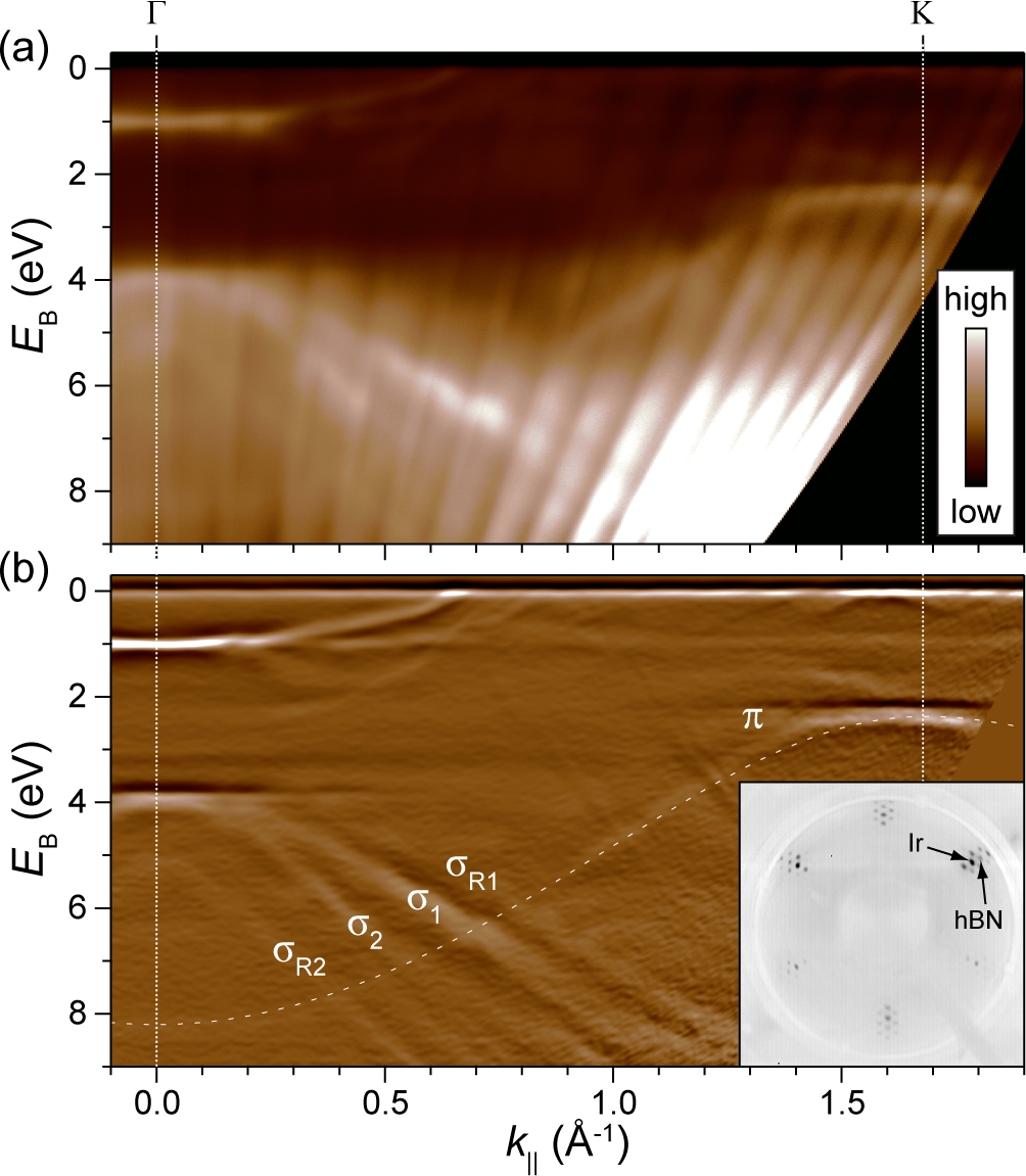
As a starting point for Li deposition experiments, epitaxial hBN samples were prepared. ARPES mapping of hBN/Ir(111) in the direction, shown in Fig. 1, provides proof of good quality of hBN, with , and bands visible. The replicated bands ( and ) are also evident, indicating that a well-defined moiré corrugation is present in the hBN/Ir(111) system (Usachov2012, ), again signaling for a very good uniformity of hBN over mesoscopic scales. For the sake of completeness, we fit the measured band with the first-nearest-neighbor tight binding approximation (1NN TBA) (Sawinska2010, ; Ribeiro2011a, ). Such fitting which provides boron and nitrogen onsite energies of 3.73 and -2.37 eV, respectively, and the hopping energy between the nearest neighbors of 2.78 eV (see Appendix A for more details). The fitted dispersion is plotted in Fig. 1(b) by a dashed line. Crystallographic quality of hBN has been confirmed by LEED data [see inset in Fig. 1(b)], where the diffraction satellite spots of the moiré structure surround the first order Ir and hBN spots.
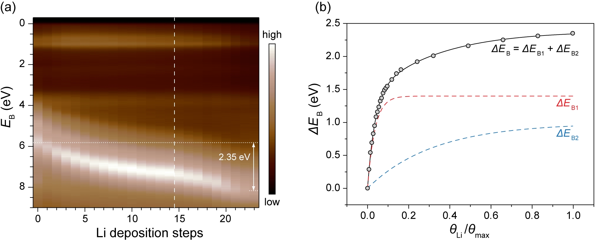
Li deposition on hBN/Ir(111) has been conducted in a series of steps. Due to the limited photon energy and the respective restrictions in the size of -space available in our experiments, focus is put on the bands and evolution of their binding energy as a function of the deposited Li amount (). A stack of energy distribution curves (EDCs) extracted at Å-1 is shown in a color plot in Fig. 2(a). At first, Li was deposited in 1-minute-long steps, and subsequently in 2-, 4- and 6-minutes-long steps [data right of the dashed line in Fig. 2(a)] in order to reach the maximum shift of the bands more efficiently. The downshift of the bands, i.e., the increase of their binding energies is evident. Initially, the shift progresses relatively fast, but afterwards it slows down and eventually saturates at a value of 2.35 eV. This is visible from the comparison of band position in consecutive EDCs: employment of 1-minute-long steps induces progressively diminishing shift (up to the deposition step 14), and only utilization of longer, i.e., 2-, 4- and 6-minutes-long steps (deposition step 15 and beyond) allows for a distinction of further shift of the bands. Such observation points to a non-linear shift of the bands as a function of number of Li deposition steps and the cumulative amount of deposited Li. Application of additional Li deposition steps, beyond the ones shown in 2(a), did not produce further shift of the bands. Instead, it resulted in blurring and reduction of photoemission intensity of the bands, which might stem from Li multilayer formation on top of hBN.
Electronic bands that do not show a change in binding energy in Fig. 2(a) originate from Ir. The most notable bands are the ones located at eV below the Fermi level. These bands show a decrease in intensity as the number of Li deposition steps increases, which can be explained by attenuation of Ir photoelectrons due to passage through additional Li layers (similar trend is found for the bands intensity). It should be noted that these states are Ir bulk states and not surface states (Pletikosic2010, ), and therefore their attenuation cannot be related to interaction between Ir surface atoms and deposited Li atoms.
The binding energy increase of the bands, , has been determined for each deposition step by fitting the corresponding EDC curve with a Lorentzian lineshape. Furthermore, the amount of deposited Li on the sample after each step has been calculated (i) by adopting a linear relation between Li dispenser yield and the deposition time, and (ii) by defining that induces a maximum shift of the bands observed in our experiments (see Appendix B for more details). With this data, it is possible to plot as a function of , as shown in Fig. 2(b) by gray circles, and such calibration can be used for a straightforward estimation of in other experiments based on the binding energy of hBN bands.
Due to technical restrictions, work function measurements could not be performed in our setup. It is therefore not possible to disclose whether arises merely from the Li-induced modification of the sample work function and alignment of hBN bands to the vacuum level. Hence, we consider the local electric potential induced by Li dipoles that acts on hBN () for a proper description of our system. This potential is directly proportional to the band shift, (Fedorov2015, ; Cai2018, ), implying that Fig. 2(b) can also be interpreted as graph.
Saturation of data in Fig. 2(b) suggests exponential-like shift of the hBN bands as Li deposition progresses. Fitting with a single exponential function yields poor results, but a fit with a two-component exponential function of the form provides an excellent agreement with the data, as indicated by a full line in Fig. 2(b). Dashed lines in Fig. 2(b) denote the two components of the fitting function, and , where the first one exhibits rapid growth () and saturation at eV, while the second component rises more slowly () and saturates at eV. At low , the component provides dominant contribution to , and after , the component becomes the source of further shift of the bands.
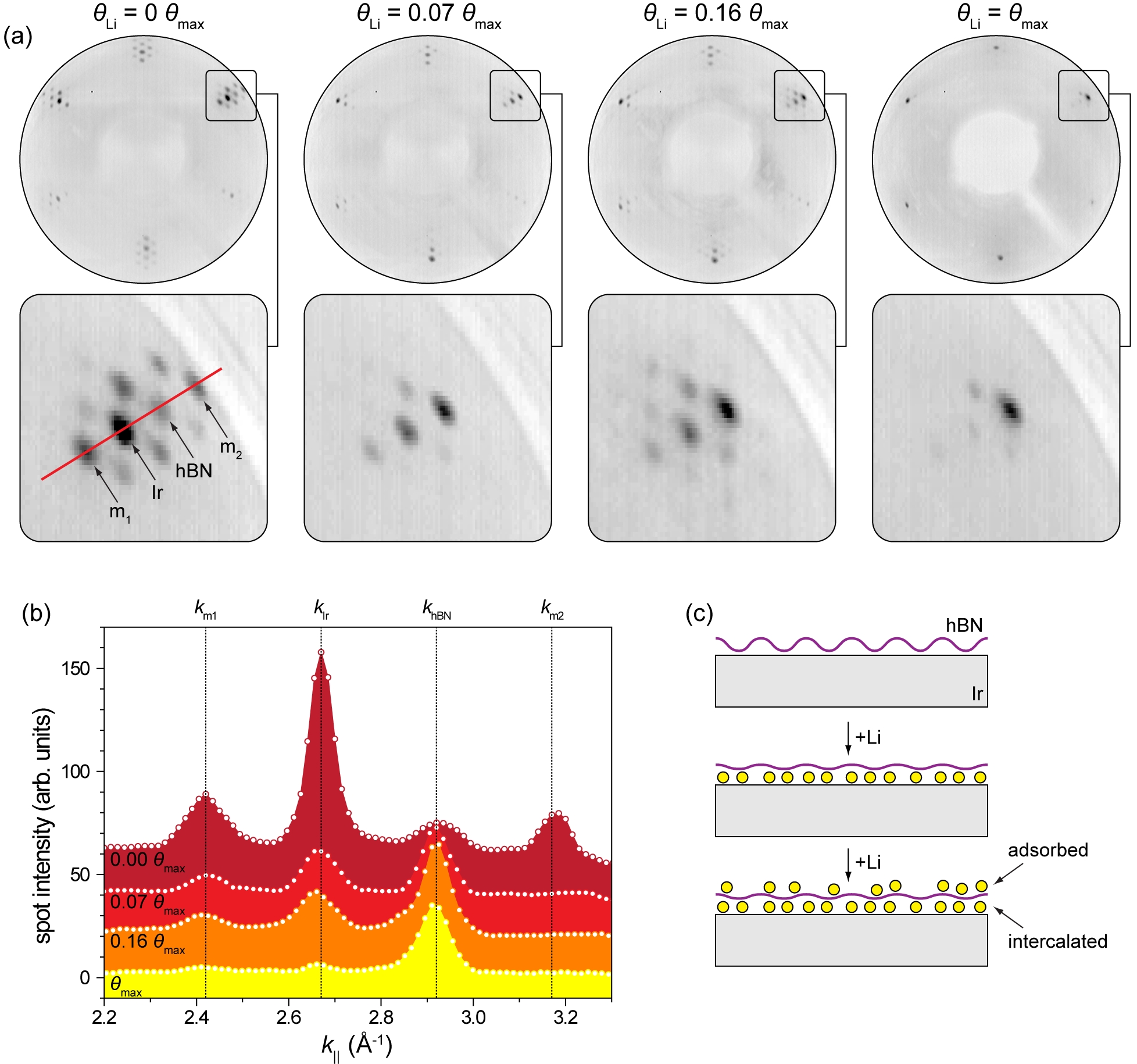
During sequential Li deposition, the diffraction pattern of the sample has been inspected several times, as shown in Fig. 3(a), upper panels. At , a diffraction pattern corresponding to the epitaxially aligned hBN on Ir(111) is observed, along with the moiré diffraction spots surrounding the first order hBN and Ir spots. A more detailed view of the moiré spots is given in the lower, zoom-in panels in Fig. 3(a). Good visibility of the moiré spots indicates significant corrugation of the hBN layer (Usachov2012, ). A cross-section through the first order hBN and Ir spots, as well as through the two closest moiré spots is given in Fig. 3(b). After deposition of only 0.07 of Li, intensity of the diffraction spots changes notably: Ir and moiré spots are significantly reduced, and the intensity of the hBN spot has increased. Additional Li deposition leads to further reduction of Ir and moiré spots, while hBN spot intensity remains approximately constant. At , moiré and Ir spots are barely visible, as evident in Figs. 3(a) and (b).
It should be noted that no Li superstructures were observed at any Li coverage. Also, an increase of the Ir spot intensity, which might indicate the formation of an intercalated superstructure (Pervan2015, ; Silva2019, ), has not been registered. Hence, we conclude that Li most likely forms disordered structures on hBN/Ir(111) at room temperature, which is in line with Li intercalation in bulk hBN (Sumiyoshi2012, ).
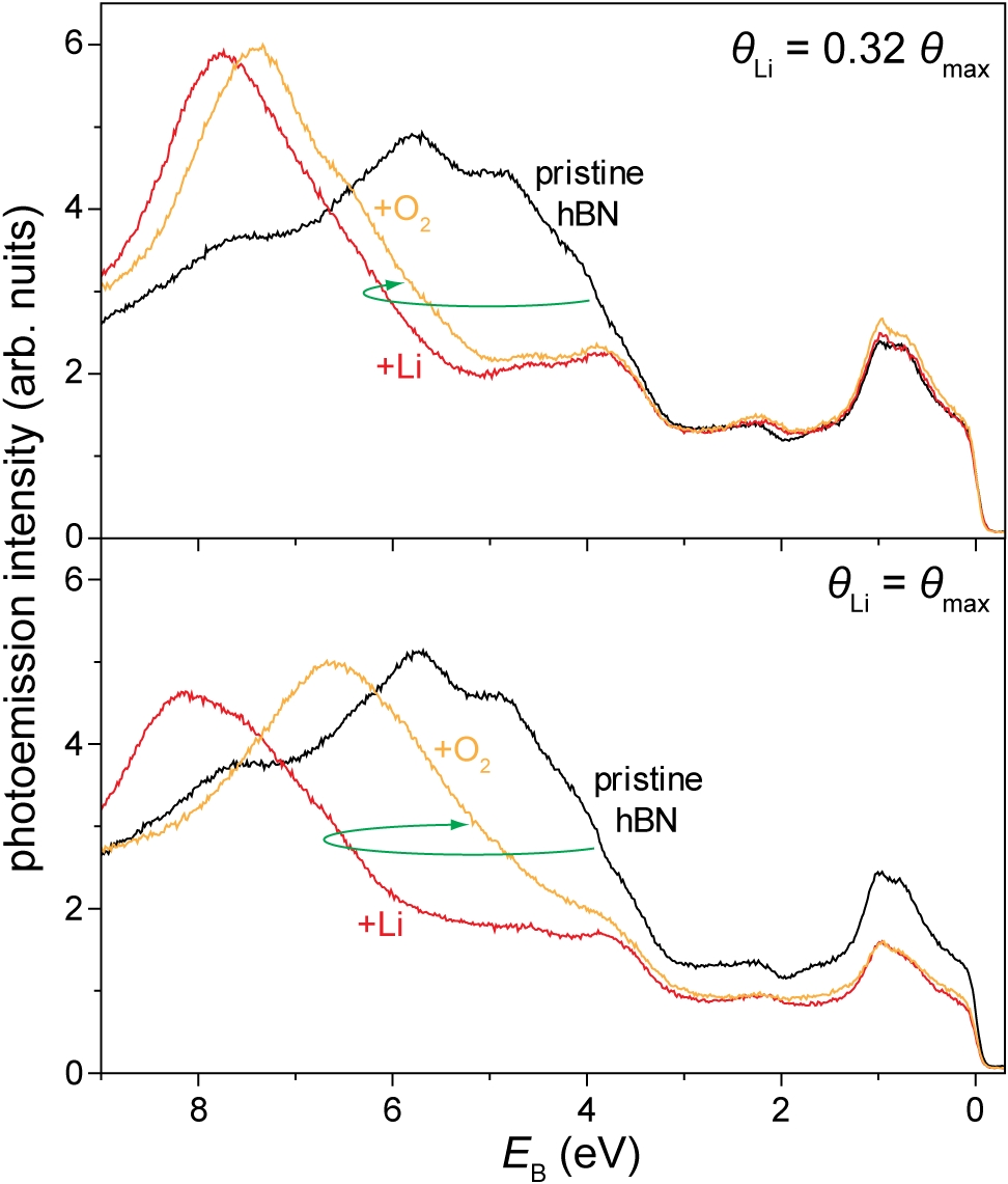
To further investigate the arrangement of Li on hBN/Ir(111), and samples have been exposed to 100 L ( mbar for 270 s) of molecular oxygen (99.999 % purity) at RT. Since alkali metals readily oxidize in such environment (Matyba2015, ), this experiment can reveal whether the alkali atoms are intercalated (therefore, protected from oxygen by hBN), adsorbed on top of hBN (i.e., exposed to oxygen), or take on some mixed intermediate configuration. The effects of O2 exposure are shown in Fig. 4 where the corresponding EDCs extracted at Å-1 are shown. For the sample, deposited Li increased the binding energy of the bands by 2 eV. Subsequent O2 exposure resulted in a 0.28 eV backshift to the Fermi level. For the sample, deposited Li increased the binding energy of the bands by 2.35 eV, i.e., by the largest amount observed in our experiments. The following O2 exposure then caused a significantly larger backshift of 1.49 eV, as illustrated in Fig. 4 by green arrows. Additional 100 L O2 exposure of the sample did not produce any additional shift of the bands. Apparently, introduction of oxygen triggers reduction of the local electric potential , and the magnitude of such reduction depends on the amount of Li that has been deposited on the sample. In agreement with Fig. 2(a), intensity of the Ir bands at eV below the Fermi level gets reduced after the deposition of of Li. Importantly, the intensity of these Ir bands is not restored upon oxygen exposure.
IV Discussion
The outlined experiments clarify spatial arrangement of Li atoms at different coverages. Reduction of the Ir and moiré spots and an increase in intensity of the hBN spots, as visible in Fig. 3(b), are typical signatures of decoupling related to the insertion of atoms between 2D material and its substrate (Ulstrup2014a, ; Pervan2015, ; Silva2019, ; Lin2018a, ). Since such LEED intensity modification has been observed already for small amounts of Li, we conclude that Li atoms initially intercalate between hBN and Ir, rather then stay adsorbed on the vacuum side of hBN.
Further elaboration of Li positioning is provided by O2 exposure experiments. Any Li atoms adsorbed on hBN are able to react with O2 molecules and form Li oxides, Li2Ox (SHEK1990, ; Pervan2017, ). In contrast to elemental Li, Li oxide does not act as an efficient electron donor. Therefore, in a system with Li2Ox present, the total amount of charge transferred to Ir is reduced in comparison to a system with elemental Li. Consequently, corresponding induced dipole magnitude, electric potential and shift of the electronic bands are also reduced. We believe this scenario is visible in Fig. 4. Exposure to O2 resulted in a backshift for both and samples as a result of Li2Ox formation on top of hBN. Therefore, the observation of a backshift indicates the presence of adsorbed Li, since hBN layer is chemically inert and its electronic structure would not be affected by the presence of O2. However, the backshift is significantly larger (approximately five times) for the sample. This is explained by a larger quantity of Li adsorbed on hBN prior to oxygen exposure, accompanied by a larger charge loss and a more pronounced electric potential reduction when Li2Ox forms. Also, the fact that Ir bands remain attenuated after O2 exposure corroborate the scenario of Li oxide formation on top of hBN, rather than oxygen-promoted removal of adsorbed Li. Intercalated Li is protected from oxidation by hBN layer (Matyba2015, ; Pervan2017, ) and is responsible for the residual electric potential causing the remaining shift of the bands. We speculate that discrepancy in the remaining shift for the two oxidized samples originates form different amounts of Li2Ox on each of them, which give rise to different dielectric surroundings.
Overall, it can be concluded that Li is initially being intercalated at the hBN-Ir interface, and starts adsorbing and accumulating on top of hBN at the later stages of deposition [see Fig. 3(c)]. Similar behavior has been found for Li deposition on graphene/Ir(111) (Petrovic2013a, ; Pervan2015, ), and is conditioned by the size of Li atoms. Having small dimensions, Li atoms require a small amount of energy to delaminate 2D materials from their substrate, and are able to intercalate already at RT. In addition, Li atoms can penetrate 2D materials even through the smallest defects which might be impermeable to other, larger atoms. Intercalation through defects is a reasonable assumption, since the migration of a Li atom through a perfect hBN mesh is energetically very expensive ( eV (Oba2010, )). Intercalated Li cations are effectively screened by the Ir substrate (Petrovic2013a, ) (see also discussion below), which additionally lowers their energy and promotes intercalation as a preferred system configuration. However, as the concentration of intercalated atoms approaches its maximum, adsorption from the vacuum side also becomes allowed.
A stepwise deposition of alkali atoms employed in our study, which has not been examined before for other similar systems (Fedorov2015, ; Cai2018, ), allows investigation of the respective charge transfer and hBN valence band shift dynamics in more detail. This dynamics, in conjunction with the conclusions about the Li positioning and the conducted fitting of with , is interpreted as follows. Initially, Li atoms form dilute intercalated structures without well-defined crystallography. In such configuration, Li atoms give a significant fraction of their 2s electrons to the Ir substrate, since the Li-Li distance is large and the corresponding Coulomb repulsion penalty is negligible. Hence, at low , Li atoms are highly charged and they give rise to rapidly increasing and . Accordingly, it is plausible that the shift of the bands induced only by the intercalated Li corresponds to the fast component . As increases, intercalated Li atoms become more closely spaced. Then, it becomes energetically unfavorable for them to be highly charged because the Coulomb repulsion between them would be large, even though the charge of Li cations is partially screened by the proximity of the metal substrate (Petrovic2013a, ). Overall, due to the Coulomb penalty and screening, the effective charge per intercalated Li atom reduces, which leads to the saturation of . In parallel, Li atoms become adsorbed on hBN, and also donate charge to Ir. The mechanism of Coulomb penalty applies to them as well, only without screening from the substrate due to the larger Li-Ir separation. The charge that adsorbed Li atoms give to Ir induces additional electric potential and the component of the overall band shift. According to Fig. 2(b), adsorbed Li becomes the dominant source of increase for .
Therefore, an increase of Li coverage inevitably leads to a progressive reduction of the charge transferred from each Li atom to Ir (in both the intercalated and the adsorbed subsystems) and also screening of Li atoms (in the intercalated subsystem). Such charge transfer dynamics results in a continuously diminishing increase, and eventually saturation, of and , as is evident from Fig. 2(b). Indeed, it is expected that the Coulomb penalty would provide exponential saturation of and (and therefore also ), since the charge of individual Li atoms reduces proportionally to the total number of atoms in the system. In the presence of both intercalated and adsorbed Li, the respective electric potentials add up and jointly shift the electronic bands of hBN to higher binding energies, since the corresponding electric dipole fields point in the same direction towards Ir (Fedorov2015, ). Adsorbed Li atoms are not as highly charged as intercalated atoms due to the substantial separation from the metal substrate which hinders charge donation (Fedorov2015, ), and they cannot induce as large shifts of the electronic bands as intercalated Li atoms do initially. However, the presence of adsorbed Li atoms provides additional, slowly increasing electric potential which pushes the bands further to yield of 2.35 eV.
V Summary
Sequential deposition of Li on hBN/Ir(111) results in a stepwise shift of the electronic bands of hBN to higher binding energies. The shift is proportional to the magnitude of the electric potential acting on the electrons of hBN, where the source of the potential are electric dipoles arising from the charge transferred from Li to Ir. In the initial stages of deposition, Li atoms get intercalated in a disordered structure and decouple hBN from its substrate. Once intercalated, Li atoms are highly charged, and they give rise to a significant (up to 1.4 eV) and fast-progressing shift of the electronic bands. As the deposition continues, Li also adsorbs on top of hBN, from where it induces additional, somewhat smaller shift of the bands (up to 1 eV) that is characterized by a moderate increase rate. Overall, the shift progresses rapidly in the beginning, slows down as the deposition advances and eventually saturates at a maximum Li coverage studied. The main reasons for the observed dynamics of valence band shift are the facilitated charge transfer from intercalated Li atoms in comparison to adsorbed Li atoms, the Coulomb repulsion penalty (for intercalated and adsorbed Li) and screening from the substrate (for intercalated Li). These factors all together cause progressive reduction of the charge transferred per Li atom to Ir and reduction of the respective electric potential. The presented results shed new light onto the interaction of epitaxial hBN with charged species and describe the response of its electronic bands to variable electric potentials, and as such can be beneficial for optimization of chemical functionalization and electric gating of hBN.
Acknowledgements.
Financial support by the Center of Excellence for Advanced Materials and Sensing Devices (ERDF Grant KK.01.1.1.01.0001) and by the Alexander von Humboldt foundation is acknowledged.Declaration of competing interests
The author declares no competing financial interests.
Appendix: TBA fitting and Li coverage calibration
A. TBA fitting
A good description of the bands of hBN can be obtained form tight binding approximation (TBA). By taking into account only the first nearest neighbors, the dispersion of the bands can be described by (Sawinska2010, ; Ribeiro2011a, )
| (A1) |
| (A2) |
where and are the onsite energies at the boron and nitrogen atoms, is the hopping energy between nearest neighbors, is the lattice parameter of hBN, and is the electron in-plane wavevector. Fitting of the experimentally measured hBN bands with TBA models is often avoided in the literature due to the inability to access the unoccupied conduction band, i.e., to measure the quasiparticle band gap of epitaxial hBN. However, in order to provide a quantitative description of the band, we accept a simplistic assumption that the quasiparticle band gap of monolayer hBN on Ir(111) () corresponds to the optical band gap of hBN monolayer on graphite and equals 6.1 eV (Elias2019, ). After setting the lattice parameter to Å (FarwickZumHagen2016, ), fitting the ARPES data at and K points with Eqs. A1 and A2 provides eV, eV, and eV. The fitted value of the hopping parameter is in excellent agreement with the one obtained by fitting the TBA bands to ab-initio calculations of hBN on graphene bilayer (Sawinska2010, ).
B. Li coverage calibration
Alkali metal dispensers used in the experiments exhibit time-dependent yield (alkali, ) which depends on the current used for heating the dispenser, age of the dispenser, and potentially other experimental factors as well. The amount of alkali atoms released from the dispenser per unit time increases as the deposition progresses, and this needs to be taken into account when converting Li deposition time (seconds or minutes) into Li coverage (in units of ). In practice, for example, this means that one 5-minute-long deposition step provides more Li than five consecutive 1-minute-long steps.
We conducted a series of 1- and 2-minute-long deposition steps. By analyzing the corresponding ARPES spectra and the binding energy of the bands, it was found that 13 1-minute-long steps induce the same (within the experimental error), and therefore provide the same amount of Li, as do 4 2-minute-long steps. By recognizing that Li dispenser yield, , is a linear function of time for typical deposition times used in our experiments (alkali, ), and by assuming that the sticking coefficient of Li does not change significantly during deposition, the equivalence of the two Li coverages requires
| (A3) |
to be valid. It is then straightforward to show that Li coverage can be expressed as
| (A4) |
for a sequence of Li deposition steps of duration . By defining that a particular combination of deposition steps equals to , all other Li deposition combinations can be converted to MLs.
References
- (1) K. Watanabe, T. Taniguchi, H. Kanda, Direct-bandgap properties and evidence for ultraviolet lasing of hexagonal boron nitride single crystal, Nat. Mater. 3 (2004) 404–409. doi:10.1038/nmat1134.
- (2) M. Corso, W. Auwärter, M. Muntwiler, A. Tamai, T. Greber, J. Osterwalder, Boron nitride nanomesh, Science 303 (2004) 217–220. doi:10.1126/science.1091979.
- (3) A. Pakdel, Y. Bando, D. Golberg, Nano boron nitride flatland, Chem. Soc. Rev. 43 (2014) 934–959. doi:10.1039/C3CS60260E.
- (4) C. R. Dean, A. F. Young, I. Meric, C. Lee, L. Wang, S. Sorgenfrei, K. Watanabe, T. Taniguchi, P. Kim, K. L. Shepard, J. Hone, Boron nitride substrates for high-quality graphene electronics, Nat. Nanotechnol. 5 (2010) 722–726. doi:10.1038/nnano.2010.172.
- (5) G.-H. Lee, X. Cui, Y. D. Kim, G. Arefe, X. Zhang, C.-h. Lee, F. Ye, K. Watanabe, T. Taniguchi, P. Kim, J. Hone, Highly Stable, Dual-Gated MoS2 Transistors Encapsulated by Hexagonal Boron Nitride with Gate-Controllable Contact, Resistance, and Threshold Voltage, ACS Nano 9 (2015) 7019–7026. doi:10.1021/acsnano.5b01341.
- (6) J. S. Ross, P. Klement, A. M. Jones, N. J. Ghimire, J. Yan, D. G. Mandrus, T. Taniguchi, K. Watanabe, K. Kitamura, W. Yao, D. H. Cobden, X. Xu, Electrically tunable excitonic light-emitting diodes based on monolayer WSe2 p-n junctions, Nat. Nanotechnol. 9 (2014) 268–272. doi:10.1038/nnano.2014.26.
- (7) M. Sajjad, G. Morell, P. Feng, Advance in Novel Boron Nitride Nanosheets to Nanoelectronic Device Applications, ACS Appl. Mater. Interfaces 5 (2013) 5051–5056. doi:10.1021/am400871s.
- (8) S. Lin, X. Li, P. Wang, Z. Xu, S. Zhang, H. Zhong, Z. Wu, W. Xu, H. Chen, Interface designed MoS2/GaAs heterostructure solar cell with sandwich stacked hexagonal boron nitride, Sci. Rep. 5 (2015) 15103. doi:10.1038/srep15103.
- (9) W. Auwärter, Hexagonal boron nitride monolayers on metal supports: Versatile templates for atoms, molecules and nanostructures, Surf. Sci. Rep. 74 (2019) 1–95. doi:10.1016/j.surfrep.2018.10.001.
- (10) A. Fedorov, C. S. Praveen, N. I. Verbitskiy, D. Haberer, D. Usachov, D. V. Vyalikh, A. Nefedov, C. Wöll, L. Petaccia, S. Piccinin, H. Sachdev, M. Knupfer, B. Büchner, S. Fabris, A. Grüneis, Efficient gating of epitaxial boron nitride monolayers by substrate functionalization, Phys. Rev. B 92 (2015) 125440. doi:10.1103/PhysRevB.92.125440.
- (11) J. Cai, W. Jolie, C. C. Silva, M. Petrović, C. Schlueter, T. Michely, M. Kralj, T.-L. Lee, C. Busse, Modifying the geometric and electronic structure of hexagonal boron nitride on Ir(111) by Cs adsorption and intercalation, Phys. Rev. B 98 (2018) 195443. doi:10.1103/PhysRevB.98.195443.
- (12) R. J. Koch, J. Katoch, S. Moser, D. Schwarz, R. K. Kawakami, A. Bostwick, E. Rotenberg, C. Jozwiak, S. Ulstrup, Electronic structure of exfoliated and epitaxial hexagonal boron nitride, Phys. Rev. Mater. 2 (2018) 074006. doi:10.1103/PhysRevMaterials.2.074006.
- (13) F. Späth, H. R. Soni, J. Steinhauer, F. Düll, U. Bauer, P. Bachmann, W. Hieringer, A. Görling, H. Steinrück, C. Papp, Oxygen Functionalization of Hexagonal Boron Nitride on Ni(111), Chem. Eur. J. 25 (2019) 8884–8893. doi:10.1002/chem.201901504.
- (14) F. Zhang, K. Németh, J. Bareño, F. Dogan, I. D. Bloom, L. L. Shaw, Experimental and theoretical investigations of functionalized boron nitride as electrode materials for Li-ion batteries, RSC Adv. 6 (2016) 27901–27914. doi:10.1039/C6RA03141B.
- (15) I. Lončarić, Z. Rukelj, V. M. Silkin, V. Despoja, Strong two-dimensional plasmon in Li-intercalated hexagonal boron-nitride film with low damping, npj 2D Mater. Appl. 2 (2018) 33. doi:10.1038/s41699-018-0078-y.
- (16) Y.-m. Ding, J.-j. Shi, M. Zhang, X.-h. Jiang, H.-x. Zhong, P. Huang, M. Wu, X. Cao, Improvement of n-type conductivity in hexagonal boron nitride monolayers by doping, strain and adsorption, RSC Advances 6 (2016) 29190–29196. doi:10.1039/C5RA25141A.
- (17) M. Petrović, U. Hagemann, M. Horn-von Hoegen, F.-J. Meyer zu Heringdorf, Microanalysis of single-layer hexagonal boron nitride islands on Ir(111), Appl. Surf. Sci. 420 (2017) 504–510. doi:10.1016/j.apsusc.2017.05.155.
- (18) D. Usachov, A. Fedorov, O. Vilkov, V. K. Adamchuk, L. V. Yashina, L. Bondarenko, A. A. Saranin, A. Grüneis, D. V. Vyalikh, Experimental and computational insight into the properties of the lattice-mismatched structures: Monolayers of h-BN and graphene on Ir(111), Phys. Rev. B 86 (2012) 155151. doi:10.1103/PhysRevB.86.155151.
- (19) J. Sławińska, I. Zasada, Z. Klusek, Energy gap tuning in graphene on hexagonal boron nitride bilayer system, Phys. Rev. B 81 (2010) 155433. doi:10.1103/PhysRevB.81.155433.
- (20) R. M. Ribeiro, N. M. R. Peres, Stability of boron nitride bilayers: Ground-state energies, interlayer distances, and tight-binding description, Phys. Rev. B 83 (2011) 235312. doi:10.1103/PhysRevB.83.235312.
- (21) I. Pletikosić, M. Kralj, D. Šokčević, R. Brako, P. Lazić, P. Pervan, Photoemission and density functional theory study of Ir(111): energy band gap mapping, J. Phys.: Condens. Matter 22 (2010) 135006. doi:10.1088/0953-8984/22/13/135006.
- (22) P. Pervan, P. Lazić, M. Petrović, I. Šrut Rakić, I. Pletikosić, M. Kralj, M. Milun, T. Valla, Li adsorption versus graphene intercalation on Ir(111): From quenching to restoration of the Ir surface state, Phys. Rev. B 92 (2015) 245415. doi:10.1103/PhysRevB.92.245415.
- (23) C. C. Silva, J. Cai, W. Jolie, D. Dombrowski, F. H. Farwick zum Hagen, A. J. Martínez-Galera, C. Schlueter, T.-L. Lee, C. Busse, Lifting Epitaxial Graphene by Intercalation of Alkali Metals, J. Phys. Chem. C 123 (2019) 13712–13719. doi:10.1021/acs.jpcc.9b02442.
- (24) A. Sumiyoshi, H. Hyodo, K. Kimura, Structural analysis of Li-intercalated hexagonal boron nitride, J. Solid State Chem. 187 (2012) 208–210. doi:10.1016/j.jssc.2012.01.002.
- (25) P. Matyba, A. Carr, C. Chen, D. L. Miller, G. Peng, S. Mathias, M. Mavrikakis, D. S. Dessau, M. W. Keller, H. C. Kapteyn, M. Murnane, Controlling the electronic structure of graphene using surface-adsorbate interactions, Phys. Rev. B 92 (2015) 041407. doi:10.1103/PhysRevB.92.041407.
- (26) S. Ulstrup, M. Andersen, M. Bianchi, L. Barreto, B. Hammer, L. Hornekær, P. Hofmann, Sequential oxygen and alkali intercalation of epitaxial graphene on Ir(111): enhanced many-body effects and formation of pn -interfaces, 2D Mater. 1 (2014) 025002. doi:10.1088/2053-1583/1/2/025002.
- (27) Y. Lin, Y. Li, J. T. Sadowski, W. Jin, J. I. Dadap, M. S. Hybertsen, R. M. Osgood, Excitation and characterization of image potential state electrons on quasi-free-standing graphene, Phys. Rev. B 97 (2018) 165413. doi:10.1103/PhysRevB.97.165413.
- (28) M. Shek, J. Hrbek, T. Sham, G.-Q. Xu, A soft X-ray study of the interaction of oxygen with Li, Surf. Sci. 234 (1990) 324–334. doi:10.1016/0039-6028(90)90564-O.
- (29) P. Pervan, P. Lazić, Adsorbed or intercalated: Na on graphene/Ir(111), Phys. Rev. Mater. 1 (2017) 044202. doi:10.1103/PhysRevMaterials.1.044202.
- (30) M. Petrović, I. Šrut Rakić, S. Runte, C. Busse, J. T. Sadowski, P. Lazić, I. Pletikosić, Z.-H. Pan, M. Milun, P. Pervan, N. Atodiresei, R. Brako, D. Šokčević, T. Valla, T. Michely, M. Kralj, The mechanism of caesium intercalation of graphene, Nat. Commun. 4 (2013) 2772. doi:10.1038/ncomms3772.
- (31) F. Oba, A. Togo, I. Tanaka, K. Watanabe, T. Taniguchi, Doping of hexagonal boron nitride via intercalation: A theoretical prediction, Phys. Rev. B 81 (2010) 075125. doi:10.1103/PhysRevB.81.075125.
- (32) C. Elias, P. Valvin, T. Pelini, A. Summerfield, C. J. Mellor, T. S. Cheng, L. Eaves, C. T. Foxon, P. H. Beton, S. V. Novikov, B. Gil, G. Cassabois, Direct band-gap crossover in epitaxial monolayer boron nitride, Nat. Commun. 10 (2019) 2639. doi:10.1038/s41467-019-10610-5.
- (33) F. H. Farwick zum Hagen, D. M. Zimmermann, C. C. Silva, C. Schlueter, N. Atodiresei, W. Jolie, A. J. Martínez-Galera, D. Dombrowski, U. A. Schröder, M. Will, P. Lazić, V. Caciuc, S. Blügel, T.-L. Lee, T. Michely, C. Busse, Structure and Growth of Hexagonal Boron Nitride on Ir(111), ACS Nano 10 (2016) 11012–11026. doi:10.1021/acsnano.6b05819.
- (34) SAES getters product broschure (2007), available at www.saesgetters.com, Alkali metal dispensers.