Topologically protected gap states and resonances in gated trilayer graphene
Abstract
Gated trilayer graphene exhibits energy gap in its most stable ABC stacking. Here we show that when the stacking order changes from ABC to CBA, three gapless states appear in each valley. The states are topologically protected and their number is related to the change of the valley Chern number across the stacking boundary. The stacking change is achieved by corrugation or delamination in the top and bottom layers, which simultaneously yields two AB/BA stacking domain walls in the pairs of adjacent layers (in bilayers). This in turn causes that for some gate voltages two pairs of topological resonances appear additionally in the conduction and valence band continua.
pacs:
73.63.-b, 72.80.VpI Introduction
Bilayer graphene (BLG) with AB stacking order of sublattices opens tunable energy gap under applied gate voltage Ohta_2006 ; Castro_2007 ; Oostinga_2008 ; Zhang_2009 . Similarly, gated trilayer graphene (TLG) also shows energy gap in its most stable ABC stacking Zhang_PRB_2010 ; Liu_np_2011 . Both systems focus attention as possible candidates for graphene-based electronics Schwierz_2010 ; Choi_2010 ; Santos_2012 ; Zhang_transistor_2018 , also due to superconductivity reported recently in BLG and TLG with twisted layers Jarillo2018 ; Chen_Nature_2019 ; Chittari_PRL_2019 .
Gated bilayer graphene presents an interesting property: when the stacking order changes from AB to BA, topological valley-protected states appear in the energy gap, connecting the conduction and valence band continua Vaezi_2013 ; Zhang_2013 ; Alden_2013 ; San_Jose_2014 ; Pelc_2015 ; Yin_NC_2016 . These states are localized at the stacking domain wall (SDW) and can provide one-dimensional currents along the SDW Ju_2015 ; Li_2016 . The stacking change may occur in the BLG when one layer is stretched, corrugated or delaminated Lin_2013 ; Ju_2015 ; Pelc_2015 ; Peeters_2018 , or even when it contains grain boundaries Jaskolski_2016 . Valley-protected states occur also in the gap of BLG and TLG when the gate polarity changes sign Martin_2008 ; Zhang_2013 ; Jung_PRB_2011 .
In this paper we investigate the electronic structure of gated trilayer graphene with stacking domain walls. We demonstrate that when the stacking order changes from ABC to CBA, three topologically protected states appear in each valley. This result is obtained by calculating the local density of states (LDOS) at stacking boundaries. Then it is confirmed by the analysis of the valley Chern number. We calculate its value and show that it changes by three when the stacking of trilayer graphene changes from ABC to CBA. We also demonstrate that for some values of the gate voltage, topologically protected resonances appear in the conduction and valence band continua, with properties characteristic for gapless states of gated bilayer with AB/BA stacking domain wall.
Two upper or two lower layers of TLG can be seen as graphene bilayers. If AB/BA stacking change is created in one of these bilayers by, for example, stretching or corrugating the upper layer only, the stacking of TLG changes from ABC to ABA. However, trilayer graphene in the ABA stacking is not gapped even under gate voltage Koshino_2009 ; Zou_nl_2013 ; Zhang_2013 . To achieve ABC/CBA stacking change in TLG, the AB/BA-type stacking domain walls have to be created in both bilayers. This can be achieved by simultaneous stretch or corrugation (delamination) in both, the lower and the upper layers of TLG.
It is of importance to recognize multilayer graphene systems gapped under applied electric field with topological gapless states. Such states can provide one-dimensional currents along defined directions and thus can be useful in graphene-based electronics.
II Model and methods
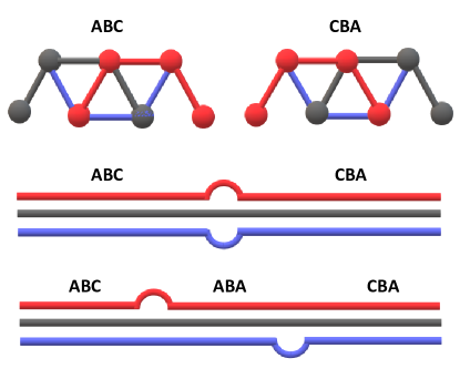
We investigate trilayer graphene in which the upper and the lower layers are corrugated, as schematically shown in the middle and bottom panels of Fig. 1. In the upper panel the 12-atom unit cells of ABC and CBA trilayers are shown. The corrugations come down to delamination of one layer versus the neighboring one Pelc_2015 , what leads to the AB/BA stacking change in a given bilayer. We call stacking domain wall in the upper bilayer as UBSDW, and stacking domain wall created in the lower bilayer as LBSDW. The presence of UBSDW and LBSDW leads automatically to the stacking change between the upper and lower layer, although they are not directly connected. We consider the smallest corrugations possible, i.e., delaminating only one unit cell in the lower layer and half a unit cell in the upper layer. It was shown in Ref.Pelc_2015 that the appearance of topological gapless states is determined by the presence of SDW, not by the size of the corrugation. The system is infinite in both, the armchair and the zigzag directions, the corrugation and thus SDW are along the zigzag direction.
Two different cases are investigated, (a) when UBSDW and LBSDW spatially overlap, and (b) when they are separated by seven unit cells, as shown in Fig. 1. In the latter case, ABA trilayer is formed between both SDWs. In both cases we study how the structure of gapless states depends on the value of the gate voltage.
We work within the -electron tight binding approximation. Intra-layer and inter-layer hopping parameters eV and eV are used, respectively Castro_2007 ; Ohta_2006 . Voltages and are applied to the bottom and top layers, respectively. Two values of are taken into account, and . This choice is dictated by the observation that topological gapless states in BLG with stacking domain walls localize in different layers depending on the value of vs Jaskolski_2018 . Local density of states along the zigzag direction is calculated for the region containing both UBSDW and LBSDW and several unit cells to the left and to the right from the corrugations (as shown in Fig. 1). To calculate LDOS we use the surface Green function matching technique Datta ; Nardelli_1999 .
III Results
III.1 Numerical calculations
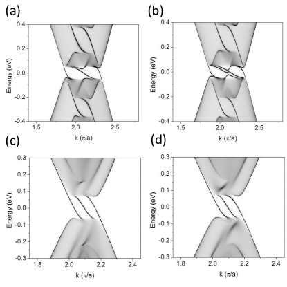
In Fig. 2 we present local density of states calculated for TLG with two minimal corrugations in the lower and upper layers, as shown in the middle and bottom panels of Fig. 1. The corrugations cause that the stacking of TLG changes from ABC (left side) to CBA (right side). Since TLG is periodic in the zigzag direction (along the corrugations) the LDOS is -dependent, where is the wavevector corresponding to this periodicity. In the upper panels of the figure, gate voltages applied to external layers are eV, while in the lower panels eV. The left panels correspond to the case of spatially overlapping LBSDW and UBSDW, right panels concern separated LBSDW and UBSDW. In all cases there are three states connecting the valence and conduction bands across the energy gap. The figure shows LDOS calculated for close to the cone at ; for the figure is mirror-reflected, so the gap states are valley-protected.
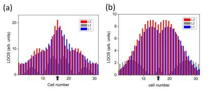
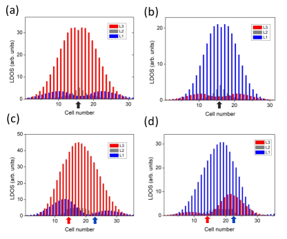
Now, we analyze the spatial localization of the gapless states. We do it first for the case of eV. In Fig. 3 (a) and (b) we present the layer-resolved LDOS calculated for -values for which line (the Fermi energy) crosses the left and right gapless states seen in Fig. 2 (a), i.e., for the case of overlapping LBSDW and UBSDW. The envelope of the vertical bars reflects the density of the corresponding wave function. For this gate voltage the states are almost entirely localized only in the lower or in the upper layer, just in place where the UBSDW and LBSDW occur. When the corrugations are separated (panels (c) and (d)) the localization of these states moves to the area between UBSDW and LBSDW. The LDOS for the middle gap state, presented in Fig. 4 (a), is almost equally distributed between the lower and the upper layers, with small contribution from the middle layer note2 . We can conclude that for this gate voltage the gapless states are due to stacking change between these two layers, which we call indirect stacking, since their nodes are not connected by .
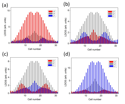
Closer inspection of Fig. 2 (a) and (b) reveals also two resonance states below and above the Fermi level, i.e., in the valence and conduction band continua. The energy structure of these resonances reminds topological gapless states of bilayer graphene Zhang_2013 ; Pelc_2015 . Indeed, the corresponding layer-resolved LDOS, shown in Fig. 5, confirm this supposition. The left resonance state in the valence band is localized in the upper layer, while the right state is localized in the middle layer, just like the gapless states of the gated upper bilayer with UBSDW Jaskolski_2018 . In the case of resonances situated in the conduction band, the left one is localized in the middle layer and the right one in the bottom layer, again, like the gapless states of the lower bilayer with LBSDW and inverted gate polarization. The appearance of resonances can be explained as follows. The gate moves the electron charge from the bottom to the middle layer, and from the middle layer to the top one. We thus get the bottom gated bilayer with the lower layer discharged - yielding two topological states in the unoccupied conduction band, and the upper gated bilayer with the top layer additionally loaded - yielding a couple of topological states in the valence band continuum. When the electron charge is not moved between the layers and the resonances do not appear (Fig. 2 c,d).

The triplet of gapless states occurs for any gate voltage. However, for , their localization is different. The layer-resolved LDOS for the left and right gap states seen in Fig. 2 (c) are presented in Fig. 6 (a) and (b), respectively; the layer-resolved LDOS of the middle gap state is visualized in Fig. 4 (b). For eV the left and right gapless states are more diffused and more evenly distributed between all three layers. We have checked that when UBSDW and LBSDW are separated, the layer mixing and diffusion are even stronger. Now, the gap states do not have the character of bilayer topological states, but reflect the global ABC/CBA stacking change in TLG.
III.2 Analysis of the valley Chern number
We begin with the Hamiltonian for trilayer graphene. Unlike the commonly applied reduced Hamiltonians for -layer graphene Min_2008 ; Jung_PRB_2011 ; Chittari_PRL_2019 , we use the full TLG Hamiltonian in its most general form. This enables direct analysis of its symmetry when the stacking changes from ABC to CBA. The final formulas show how many terms in the eigenvalue expansion are sufficient for the calculation of of the valley Chern number. For momenta close to the Dirac point , the Hamiltonian of trilayer graphene is a matrix of blocks:
| (1) |
where , and is the unit matrix, is the Fermi velocity, and is graphene lattice constant Min_2008 . Its (unnormalised) eigenvector related to the lowest energy is
| (2) |
where we use polar coordinates: and .
The valley Chern number at is defined by the Berry phase Jung_PRB_2011 ; Chittari_PRL_2019
| (3) |
with the integration performed over a circle . The calculation of yields and . To remove singularities, which appear when , we use the Rayleigh-Schrödinger perturbation theory (with the zero-order Hamiltonian ). We account up to the second correction (of the order ) and get that . The leading term in gives , while the leading term in is equal . Hence, the Berry phase is equal to and the contribution to the Chern number from is Jung_PRB_2011 ; Chittari_PRL_2019 .
Switching from to causes transposition of the matrix in the Eq. (1), which is equivalent to parity change and yields the opposite sign of the valley Chern number at . The switching from ABC to CBA stacking causes transposition of the matrix . Composition of these switchings is equivalent to a unitary symmetry on the Hamiltonian. This means that in case of CBA stacking, the contributions from neighbourhoods of and to the Chern number are and , respectively, i.e., they have reversed signs comparing to the ABC stacking. Therefore, the stacking change causes change of the local Chern number contribution by and thus the appearance of three gapless states localized at the stacking domain wall.
It is worth noting that can be unitarily transformed to , i.e., with the sign of reversed. This means that three gapless states appear also when the gate polarization changes, as was shown in Ref. Jung_PRB_2011 .
IV Conclusions
We have investigated gated trilayer graphene in the ABC stacking. We have shown that by simultaneous corrugation or delamination in the upper and lower layers, the stacking may change from ABC to CBA. This change automatically creates AB/BA-type stacking changes in the upper bilayer formed by the upper and middle layers, in the lower bilayer formed by the middle and lower layers, as well as between the upper and the lower layer, which is the indirect stacking change, since these layers are not directly connected by the interlayer hopping.
We have calculated the LDOS along the stacking domain walls and demonstrated the presence of three valley-protected topological states in the energy gap. We have analyzed the valley Chern number for TLG and shown that it changes from -3/2 to 3/2 when the stacking changes from ABC to CBA, yielding three gapless states in the energy gap at each valley.
The gapless states are robust and independent on the voltage applied to the external layers, but their distribution between the layers depends on . When is greater than the interlayer hopping the gapless states localize almost exclusively in the external layers, what means that they are due to indirect stacking change between these layers. For this voltage two pairs of topological resonance states appear additionally in the valence and conduction bands, with the characteristics typical for bilayers with SDW. When the resonance states disappear and the gapless states are more evenly distributed between all three layers. We can conclude that one-dimensional currents provided by the gap states can flow in the surface layers only, or in the entire trilayer graphene, depending on the gate voltage applied.
The appearance of topological gapless states and resonances in gated trilayer graphene with stacking change has not been reported so far. We strongly believe that these findings are important both for better understanding of the fundamental features of multilayer graphene, and for potential applications of such systems in graphene-based electronics.
References
- [1] T. Ohta, A. Bostwick, T. Seyller, K. Horn, and E. Rotenberg, Science 313, 951 (2006).
- [2] E. V. Castro, K. S. Novoselov, S. V. Morozov, N. M. R. Peres, J. M. B. L. dos Santos, J. Nilsson, F. Guinea, A. K. Geim, and A. H. C. Neto, Phys. Rev. Lett. 99, 216802 (2007).
- [3] J. B. Oostinga, H. B. Heersche, X. Liu, A. F. Morpurgo, and L. M. K. Vandersypen, Nature Materials 7, 151 (2008).
- [4] Y. Zhang, T.-T. Tang, C. Girit, Z. Hao, M. C. Martin, A. Zettl, M. F. Crommie, Y. R. Shen, and F. Wang, Nature (London) 459, 820 (2009).
- [5] F. Zhang, B. Sahu, H. Min, and A. H. McDonald, Phys. Rev. B 82, 035409 (2010).
- [6] C. H. Lui, Z. Li, K. F. Mak, E. Cappulleti, and T. F. Heinz, Nat. Phys. 7, 944 (2011).
- [7] F. Schwierz, Nat. Nanotechnol. 5, 487 (2010).
- [8] S.-M. Choi, S.-H.Jhi, and Y.-W. Son, Nano Letters 10, 3486 (2010).
- [9] H. Santos, A. Ayuela, L. Chico, and E. Artacho, Phys. Rev. B 85, 245430 (2012).
- [10] Q. Zhang, Y. Yaofeng, K. S. Chan, Z. Mu, and J. Li, App. Phys. Express 1, 075104 (2018).
- [11] Y. Cao, V. Fatemi, S. Fang, K. Watanabe, T. Taniguchi, E. Kaxiras, and P. Jarillo-Herrero, Nature 556, 43 (2018).
- [12] E. Chen, A. L. Sharpe, P. Gallagher, I. T. Rosen, E. J. Fox, L. Jiang, B. Lyou, H. Li, K. Watanabe, T. Taniguchi, J. Jung, Z. Shi, D. Goldhaber-Gordon, Y. Zhang, and F. Weng, Nature 572, 215 (2019).
- [13] B. L. Chittari, G. Chen, Y. Zhang, F. Wang, and J. Jung, Phys. Rev. Lett. 122, o16401 (2019).
- [14] A. Vaezi, Y. Liang, D. H. Ngai, L. Yang, and E.-A. Kim, Phys. Rev. X 3, 021018 (2013).
- [15] F. Zhang, A. H. MacDonald, and E. J. Male, Proc. Natl. Acad. Sci. U.S.A. 110, 10546 (2013).
- [16] J. S. Alden, A. W. Tsen, P. Y. Huang, R. Hovden, L. Brown, J. Park, D. A. Muller, and P. L McEuen, Proc. Natl. Acad. Sci. 110, 11256 (2013).
- [17] P. San-Jose, R. V. Gorbachev, A. K. Geim, K. S. Novoselov, and F. Guinea, Nano Lett. 14, 2052 (2014).
- [18] M. Pelc, W. Jaskolski, A. Ayuela, and L. Chico, Phys. Rev. B 92, 085433 (2015).
- [19] L.-J. Yin, H. Jiang, J.-B. Qiao, and L. He, Nat. Commun. 7, 11760 (2016).
- [20] L. Ju, Z. Shi, N. Nair, Y. Lv, C. Jin, J. Velasco Jr, C. Ojeda-Aristizabal, H. A. Bechtel, M. C. Martin, and A. Zettl, Nature 520, 650 (2015).
- [21] J. Li, K. Wang, K. J. MvFaul, Z. Zern, Y. Ren, K. Watanabe, T. Taniguchi, Z. Qiao, and J. Zhu, Nat. Nanotechnol. 11, 1060 (2016).
- [22] J. Lin, W. Fang, W. Zhou, A. R. Lupini, J. C. Idrobo, J. Kong, S. J. Pennycook, and S. T. Pantelides, Nano Lett. 13, 3262 (2013).
- [23] T. L. M. Lane, M. Andelkovic, J. R. Wallbank, L. Covaci, F. M. Peeters, and V. I. Falko, Phys. Rev. B 97, 045301 (2018).
- [24] W. Jaskolski, M. Pelc, L. Chico, and A. Ayuela, Nanoscale 8, 6079 (2016).
- [25] I. Martin, Y. M. Blanter, and A. F. Morpurgo, Phys. Rev. Tell. 100, 036804 (2008).
- [26] J. Jung, F. Zhang, Z. Qiao, and A. H. MacDonald, Phys. Rev. B 84, 075418 (2011).
- [27] W. Jaskolski, M. Pelc, G. W. Bryant, L. Chico, and A. Ayuela, 2D Materials 5, 025006 (2018).
- [28] M. Koshino and E. McCann, Phys. Rev. B 79, 125443 (2009).
- [29] K. Zou, F. Zhang, C. Clapp, A. H. McDonald, and J. Zhu, Nano Lett. 13, 369 (2013).
- [30] S. Datta, Electronic Transport in Mesoscopic Systems, Cambridge University Press, Cambridge, (1995).
- [31] M. B. Nardelli, Phys. Reb. B 60, 7828 (1999).
- [32] H. Min and A. H. MacDonald, Prog. Theor. Phys. Suppl. 176, 227 (2008).
- [33] F. Zhang, J. Jung, G.A. Fiete, Q. Niu, and A.H.MacDonald, Phys. Rev. Lett. 106, 156801 (2011).
- [34] Fig. 2 b reveals a couple of states detaching from the valence and conduction band continua. They originate from the ABA section of TLG, which is gapless, and appear faster in the gap when .