Swapping Exchange and Spin-Orbit Coupling in 2D van der Waals Heterostructures
Abstract
The concept of swapping the two most important spin interactions—exchange and spin-orbit coupling—is proposed based on two-dimensional multilayer van der Waals heterostructures. Specifically, we show by performing realistic ab initio simulations, that a single device consisting of a bilayer graphene sandwiched by a 2D ferromagnet Cr2Ge2Te6 (CGT) and a monolayer WS2, is able not only to generate, but also to swap the two interactions. The highly efficient swapping is enabled by the interplay of gate-dependent layer polarization in bilayer graphene and short-range spin-orbit and exchange proximity effects affecting only the layers in contact with the sandwiching materials. We call these structures ex-so-tic, for supplying either exchange (ex) or spin-orbit (so) coupling in a single device, by gating. Such bifunctional devices demonstrate the potential of van der Waals spintronics engineering using 2D crystal multilayers.
Introduction.
Novel 2D van der Waals heterostructures give a strong push to spintronics Zutic2004:RMP ; Han2014:NN ; Avsar2019:arxiv which requires electrical control of spin interactions to realize devices such as spin transistors Datta1990:APL ; Schliemann2003:PRL ; Wunderlich2010:S ; Betthausen2012:S ; Chuang2015:NN . The past years have seen impressive progress in tuning spin-orbit and exchange couplings individually Wang2015:NC ; Avsar2017:ACS ; Luo2017:NL ; Zhong2020:NN ; Karpiak2019:arxiv ; Ghiasi2017:NL ; Ghiasi2019:NL ; Ghazaryan2018:NE ; Safeer2019:NL ; Zutic2019:MT ; Benitez2020:NM ; Cortes2019:PRL ; Zihlmann2018:PRB . A particularly suitable platform for gating proximity effects is based on bilayer graphene (BLG). It was proposed that spin-orbit coupling in BLG can be turned on and off on demand Gmitra2017:PRL ; Khoo2017:NL , as recently demonstrated Island2019:Nat . Similar effects have been predicted for ferromagnetic encapsulation Michetti2010:NL ; Cardoso2018:PRL ; Zollner2018:NJP . The next milestone would be a transport demonstration with sensitivity to the spin polarization of the bands, or the spin-orbit torque in the proximity setup Alghamdi2019:NL ; Kapildeb2019:arxiv ; MacNeill2017:NP .
In this Letter we present a device structure which is capable of not only creating the two most important spin interactions—spin-orbit and exchange couplings—in an electronic system, but also swapping them on demand by an applied electric field. Being able to swap two different spin (or other effective) interactions by gating is a striking thought, without precedence in the realm of conventional materials. While proximity spin-orbit coupling preserves time-reversal symmetry, and leads to such phenomena as topological quantum spin Hall effect Kane2005:PRL or giant spin relaxation anisotropy Cummings2017:PRL ; Omar2019:PRB ; Benitez2018:NP ; Ghiasi2017:NL , proximity exchange coupling breaks time reversal symmetry and renders a nominally nonmagnetic electronic system effectively magnetic Yang2013:PRL . Swapping the two interactions provides a reversible route between time-reversal symmetric and magnetic physics.
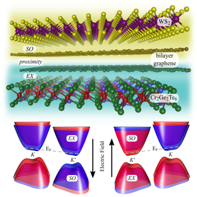
Our choice of the electronic platform for swapping the spin interactions is BLG, which is nicely suited for proximity-based devices by providing two coupled surfaces. Via layer polarization, which locks a given layer to an electronic band (or set of bands), transport properties can be strongly influenced by the environment. We use a CGT/BLG/WS2 heterostructure, with monoloayer Cr2Ge2Te6 (CGT) providing a strong proximity exchange effect to the bottom layer of BLG, and WS2 to induce strong spin-orbit coupling to the top layer, see Fig. 1.
Gating can swap spin-orbit and exchange couplings, as illustrated in Fig. 1. The applied electric field changes the layer polarization, which changes the layer-band assignment, thereby swapping the proximity exchange and spin-orbit couplings. This intuitive picture is supported below by realistic density functional theory (DFT) simulations and phenomenological modeling, predicting quantitatively the behavior of the ex-so-tic heterostructures in the presence of a transverse electric field.
Swapping spin-orbit and exchange coupling by gate.
We consider a supercell stack containing BLG sandwiched between a monolayer WS2 and a monolayer ferromagnetic CGT with an out-of-plane magnetization, as depicted in Fig. 1. We calculate the electronic states for this structure using DFT, see Supplemental Material 111See Supplemental Material including Refs. Baskin1955:PR ; Kresse1999:PRB ; Perdew1996:PRL ; Grimme2006:JCC ; Barone2009:JCC ; Bengtsson1999:PRB ; Carteaux1995:JPCM ; Gong2017:Nat ; Schutte1987:JSSC ; Zollner2018:NJP ; Gmitra2017:PRL ; Hohenberg1964:PRB ; Konschuh2012:PRB ; Island2019:Nat ; Giannozzi2009:JPCM ; Wang2019:APL ; Chen2015:PRB ; Li2014:JMCC , where we present the computational details and results for the individual BLG/CGT and WS2/BLG heterostructures. In addition, we show an animation about the electric field evolution of the low energy bands of doubly proximitized BLG. . The band structure along selected high-symmetry lines containing the point is shown in Fig. 2. The magnetization — from CGT — as well as the strong spin-orbit coupling — from the transition-metal dichalcogenide (TMDC) — are manifested by the spin polarization of the bands. Inside the semiconductor band gap, there are well preserved parabolic electronic states of BLG. States relevant for transport form the four low-energy bands close to the Fermi level. It is these four bands that are at the focus of this work.
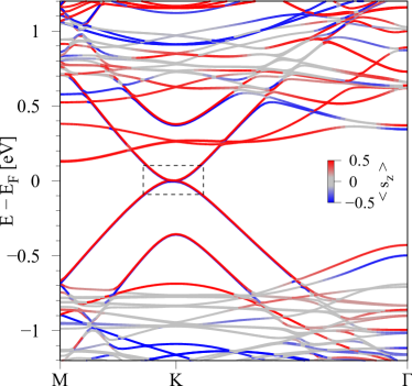
BLG per se has no band gap, has tiny spin-orbit coupling (on the order of tens of eVs Konschuh2012:PRB ), and has no magnetic exchange coupling. But sandwiched by the two monolayers, both orbital and spin properties of the low-energy bands of BLG strikingly change. First, the built-in dipole moment in the heterostructure Gmitra2017:PRL ; Zollner2018:NJP separates the conduction and valence bands, inducing a band gap for a given spin polarization. Next, the states exhibit a giant spin-orbit coupling induced from the TMDC layer. This coupling is opposite in and points, as a consequence of time reversal symmetry of the spin-orbit interaction. Finally, the electronic states of BLG become magnetic, manifested by an exchange splitting, equal in and , coming from the ferromagnetic CGT. It is the fascinating spectral separation of the spin-orbit coupling and exchange in the BLG which allows for their swapping.
The three aforementioned effects are nicely seen in Fig. 3 which shows a zoom to the low-energy band structure of the stack at both and . Perhaps the most striking feature of the band structure is the difference in the energy dispersion at and , which ultimately comes from the interplay between the induced spin-orbit and exchange couplings in BLG. While the valence and conduction bands partially overlap at , there is a local band gap at . The dipole moment of the heterostructure is too weak to open a global (over the whole Brillouin zone) band gap. The spin splittings are 2–8 meV, which is experimentally significant.
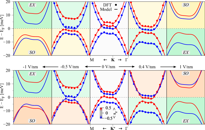
An applied external electric field increases the band gap of the doubly proximitized BLG and makes explicit the effects of the TMDC and CGT layers. This is demonstrated in Fig. 3, which shows both the DFT results (for fields , 0, and 0.4 V/nm) and model calculations (for fields, , , 0, 0.4, and 1 V/nm) using an effective Hamiltonian introduced in the next section. Let us first look at negative electric fields, say V/nm, which point down, towards CGT. The conduction bands are split by about 8 meV, having identical spin polarizations at and , which means that this splitting is due to exchange coupling: the conduction bands are affected by the ferromagnetic CGT and conduction electrons will exhibit transport properties of magnetic conductors. On the other hand, the valence bands are split less, by about 2 meV. More important, the spin polarizations of the two bands are opposite at and , signaling time-reversal symmetry: the valence bands experience spin-orbit coupling from WS2. This makes sense. At negative electric fields electrons in the upper layer of BLG have a lower energy, and form the valence band. These electrons are affected by the TMDC layer, which gives them the strong spin-orbit coupling character. We will see in the next section that the spin-orbit coupling is of the valley Zeeman type, which is characteristic for graphene proximitized by a TMDC. Similarly, electron orbitals in the lower layer of BLG have a higher energy, forming the conduction band, which is magnetic due to the presence of CGT. If the applied electric field points up, towards the TMDC layer, the situation is reversed and the spin characters of the valence and conduction bands are swapped, see Fig. 3.
We have thus demonstrated the swapping of exchange and spin-orbit couplings: at a fixed chemical potential (doping level), the electrons exhibit either exchange or spin-orbit coupling, not both. Which coupling is realized depends on the gate. The same would work with few-layer TMDCs and ferromagnetic semiconductors encapsulating BLG, since the proximity effect is sensitive to the interfacial layers only Zollner2019a:PRB .
Model Hamiltonian.
| dipole | |||||||||||
|---|---|---|---|---|---|---|---|---|---|---|---|
| 2.432 | 0.365 | -0.273 | -0.164 | -0.474 | 8.854 | 1.132 | -1.132 | -3.874 | -3.874 | 0.348 | 0.398 |
To describe the low-energy states of our heterostructure we employ a Hamiltonian for BLG in the presence of a transverse electric field Konschuh2012:PRB ,
| (1) |
It comprises orbital (orb), intrinsic spin-orbit (soc), Rashba (R), and exchange (ex) terms. We also include the Dirac-point energy shift. Below we specify the individual Hamiltonian terms using pseudospin notation. A matrix form of is given in the Supplemental Material 111See Supplemental Material including Refs. Baskin1955:PR ; Kresse1999:PRB ; Perdew1996:PRL ; Grimme2006:JCC ; Barone2009:JCC ; Bengtsson1999:PRB ; Carteaux1995:JPCM ; Gong2017:Nat ; Schutte1987:JSSC ; Zollner2018:NJP ; Gmitra2017:PRL ; Hohenberg1964:PRB ; Konschuh2012:PRB ; Island2019:Nat ; Giannozzi2009:JPCM ; Wang2019:APL ; Chen2015:PRB ; Li2014:JMCC , where we present the computational details and results for the individual BLG/CGT and WS2/BLG heterostructures. In addition, we show an animation about the electric field evolution of the low energy bands of doubly proximitized BLG. .
The orbital physics is captured by
| (2) |
where we denote the graphene lattice constant and the wave vectors and , measured from K for the valley index . The Pauli matrices , , and , represent layer, pseudospin, and spin, with . We also define and to shorten notation. Parameters , , denote intra- and interlayer hoppings of the BLG. Transverse displacement field is introduced by voltage for the lower, and for the upper layer of BLG. Finally, is the asymmetry in the energy shift of the bonding and antibonding states.
The intrinsic spin-orbit coupling term, while also present in a free-standing BLG, is strongly renormalized by the proximity to the TMDC. This effect is described by
| (3) |
with parameters denoting the proximity spin-orbit coupling of the corresponding layer () and sublattice (A, B) atom. Because of the short-rangeness of the proximity effect only the upper layer is affected, so that only parameters and are significant (on the meV scale). The Rashba coupling can emerge due to the breaking of the space inversion symmetry in the heterostructure and the applied electric field. This term has the form
| (4) |
where describes the local (intrinsic) breaking of space inversion due to the presence of the other layer in BLG. The resulting spin-orbit fields are opposite in the two layers, giving no net effect on the spin-orbit splitting. The global breaking of space inversion due to the heterostructure and the electric field is accounted for by the proper Rashba parameter . For a more detailed description of the model and parameters, we refer the reader to Ref. Konschuh2012:PRB . Finally, the magnetic proximity effect induces exchange coupling in BLG, which has the standard form,
| (5) |
where parameters represent the proximity exchange for the individual sublattices and layers.
The spectrum of the effective Hamiltonian is fitted to the DFT-obtained low-energy dispersion of doubly proximitized BLG at zero applied electric field shown in Fig. 2. First, the orbital parameters from are obtained, as well as the built-in bias , staggered potential , and the Dirac energy . In the second step we analyze the fine structure of the spectrum and extract proximity induced spin-orbit and exchange parameters. The induced spin-orbit coupling in the upper layer is of the valley-Zeeman type, with opposite parameters on the two atoms of the sublattice: meV. The atoms of the lower BLG layer experience strong proximity exchange coupling due to the adjacent CGT, meV . As for the Rashba coupling, it is negligible (on the meV scale), which is consistent with our finding that the spin polarization of the considered bands is predominantly out of plane. The fitted parameters are summarized in Table 1; parameters not presented there were found to be negligible and set to zero. With such a minimal set of parameters the agreement of the effective model and the DFT is excellent, see Fig. 3.
The fitted parameters demonstrate the message that one layer of BLG experiences giant (on the meV scale) spin-orbit coupling, while the other layer giant exchange coupling, at zero electric field. The only parameter that significantly changes when an electric field is applied is . We therefore change in our model Hamiltonian (and keep other parameters as fitted to the zero-field DFT results) to see how the spectra develop. The results are presented in Fig. 3. Their qualitative interpretation was already given above. Here we only note that the consistency of this procedure (changing only as the electric field is applied) is checked by performing DFT simulations for two electric fields, and V/nm; for V/nm we use assuming its linear dependence on the applied electric field. The agreement with the model calculations, seen in Fig. 3, gives us full confidence in our approach. More detailed fit results can be found in the Supplemental Material 111See Supplemental Material including Refs. Baskin1955:PR ; Kresse1999:PRB ; Perdew1996:PRL ; Grimme2006:JCC ; Barone2009:JCC ; Bengtsson1999:PRB ; Carteaux1995:JPCM ; Gong2017:Nat ; Schutte1987:JSSC ; Zollner2018:NJP ; Gmitra2017:PRL ; Hohenberg1964:PRB ; Konschuh2012:PRB ; Island2019:Nat ; Giannozzi2009:JPCM ; Wang2019:APL ; Chen2015:PRB ; Li2014:JMCC , where we present the computational details and results for the individual BLG/CGT and WS2/BLG heterostructures. In addition, we show an animation about the electric field evolution of the low energy bands of doubly proximitized BLG. , where we also provide results for the individual BLG/CGT and WS2/BLG subsystems, to further validate the robustness of the model.
For an experimental realization of the swapping effect it is preferred to dope BLG with holes, to prevent spilling out the conduction-band carriers into the CGT (the Dirac point is about 100 meV below the conduction band of CGT, see Fig. 2), upon application of a field. However, we do not expect such a spill-out for conduction-electrons to happen at fields lower than 0.5 V/nm Zollner2018:NJP .
Summary.
Doubly proximitized BLG offers a unique platform for investigating fundamental spin physics and designing multifunctional spintronics applications. Using realistic DFT simulations and phenomenological modeling we demonstrate swapping the two most important spin interactions — exchange and spin-orbit couplings — in a WS2/BLG/CGT multilayer. The swapping also means turning the time-reversal symmetry on and off, on demand, in the electronic states at a given doping. Since the effect is robust, we expect a variety of swapping phenomena if the bilayer sandwich comprises antiferromagnets, ferroelectricity, ferroelectrics, topological insulators, or superconductors.
Acknowledgements.
This work was funded by the Deutsche Forschungsgemeinschaft (DFG, German Research Foundation) SFB 1277 (Project-ID 314695032), the European Unions Horizon 2020 research and innovation program under Grant No. 785219, DFG SPP 1666, and by the VEGA 1/0105/20 and the Internal Research Grant System VVGS-2019-1227.References
- (1) Zutic, I., Fabian, J. & Das Sarma, S. Spintronics: Fundamentals and applications. Rev. Mod. Phys. 76, 323 (2004).
- (2) Han, W., Kawakami, R. K., Gmitra, M. & Fabian, J. Graphene spintronics. Nat. Nanotechnol. 9, 794 (2014).
- (3) Avsar, A. et al. Colloquium: Spintronics in graphene and other two-dimensional materials. Rev. Mod. Phys. 92, 021003 (2020).
- (4) Datta, S. & Das, B. Electronic analog of the electro‐optic modulator. Appl. Phys. Lett. 56, 665 (1990).
- (5) Schliemann, J., Egues, J. C. & Loss, D. Nonballistic Spin-Field-Effect Transistor. Phys. Rev. Lett. 90, 146801 (2003).
- (6) Wunderlich, J. et al. Spin Hall Effect Transistor. Science 330, 1801 (2010).
- (7) Betthausen, C. et al. Spin-Transistor Action via Tunable Landau-Zener Transitions. Science 337, 324 (2012).
- (8) Chuang, P. et al. All-electric all-semiconductor spin field-effect transistors. Nature Nanotechnol. 10, 35 (2015).
- (9) Wang, Z. et al. Strong interface-induced spin-orbit interaction in graphene on WS2. Nat. Commun. 6, 8339 (2015).
- (10) Avsar, A. et al. Optospintronics in Graphene via Proximity Coupling. ACS Nano 11, 11678 (2017).
- (11) Luo, Y. K. et al. Opto-valleytronic spin injection in monolayer MoS2/few-layer graphene hybrid spin valves. Nano Lett. 17, 3877 (2017).
- (12) Zhong, D. et al. Layer-resolved magnetic proximity effect in van der Waals heterostructures. Nat. Nanotechnol. (2020).
- (13) Karpiak, B. et al. Magnetic proximity in a van der Waals heterostructure of magnetic insulator and graphene. 2D Mater. 7, 015026 (2019).
- (14) Ghiasi, T. S., Ingla-Aynés, J., Kaverzin, A. A. & Van Wees, B. J. Large Proximity-Induced Spin Lifetime Anisotropy in Transition-Metal Dichalcogenide/Graphene Heterostructures. Nano Lett. 17, 7528 (2017).
- (15) Ghiasi, T. S., Kaverzin, A. A., Blah, P. J. & van Wees, B. J. Charge-to-Spin Conversion by the Rashba–Edelstein Effect in Two-Dimensional van der Waals Heterostructures up to Room Temperature. Nano Lett. 19, 5959 (2019).
- (16) Ghazaryan, D. et al. Magnon-assisted tunnelling in van der Waals heterostructures based on CrBr3. Nature Electronics 1, 344 (2018).
- (17) Safeer, C. et al. Room-temperature spin Hall effect in graphene/MoS2 van der Waals heterostructures. Nano Lett. 19, 1074 (2019).
- (18) Zutic, I., Matos-Abiague, A., Scharf, B., Dery, H. & Belashchenko, K. Proximitized materials. Mater. Today 22, 85 (2019).
- (19) Benitez, L. A. et al. Tunable room-temperature spin galvanic and spin Hall effects in van der Waals heterostructures. Nat. Mater. 19, 170 (2020).
- (20) Cortés, N., Ávalos-Ovando, O., Rosales, L., Orellana, P. A. & Ulloa, S. E. Tunable spin-polarized edge currents in proximitized transition metal dichalcogenides. Phys. Rev. Lett. 122, 086401 (2019).
- (21) Zihlmann, S. et al. Large spin relaxation anisotropy and valley-Zeeman spin-orbit coupling in /graphene/-BN heterostructures. Phys. Rev. B 97, 075434 (2018).
- (22) Gmitra, M. & Fabian, J. Proximity Effects in Bilayer Graphene on Monolayer WSe2: Field-Effect Spin Valley Locking, Spin-Orbit Valve, and Spin Transistor. Phys. Rev. Lett. 119, 146401 (2017).
- (23) Khoo, J. Y., Morpurgo, A. F. & Levitov, L. On-Demand Spin-Orbit Interaction from Which-Layer Tunability in Bilayer Graphene. Nano Lett. 17, 7003 (2017).
- (24) Island, J. O. et al. Spin-orbit-driven band inversion in bilayer graphene by the van der Waals proximity effect. Nature 571, 85 (2019).
- (25) Michetti, P., Recher, P. & Iannaccone, G. Electric field control of spin rotation in bilayer graphene. Nano Lett. 10, 4463 (2010).
- (26) Cardoso, C., Soriano, D., García-Martínez, N. A. & Fernández-Rossier, J. Van der Waals Spin Valves. Phys. Rev. Lett. 121, 067701 (2018).
- (27) Zollner, K., Gmitra, M. & Fabian, J. Electrically tunable exchange splitting in bilayer graphene on monolayer Cr2X2Te6 with X = Ge, Si, and Sn. New J. Phys. 20, 073007 (2018).
- (28) Alghamdi, M. et al. Highly Efficient Spin–Orbit Torque and Switching of Layered Ferromagnet Fe3GeTe2. Nano Lett. 19, 4400 (2019).
- (29) Dolui, K. et al. Proximity Spin-Orbit Torque on a Two-Dimensional Magnet within van der Waals Heterostructure: Current-Driven Antiferromagnet-to-Ferromagnet Reversible Nonequilibrium Phase Transition in Bilayer CrI3. Nano Lett. 20, 2288 (2020).
- (30) MacNeill, D. et al. Control of spin–orbit torques through crystal symmetry in WTe2/ferromagnet bilayers. Nature Physics 13, 300 (2017).
- (31) Kane, C. L. & Mele, E. J. Quantum Spin hall effect in graphene. Phys. Rev. Lett. 95, 226801 (2005).
- (32) Cummings, A. W., Garcia, J. H., Fabian, J. & Roche, S. Giant Spin Lifetime Anisotropy in Graphene Induced by Proximity Effects. Phys. Rev. Lett. 119, 206601 (2017).
- (33) Omar, S., Madhushankar, B. N. & van Wees, B. J. Large spin-relaxation anisotropy in bilayer-graphene/ heterostructures. Phys. Rev. B 100, 155415 (2019).
- (34) Benitez, L. A. et al. Strongly anisotropic spin relaxation in graphene-transition metal dichalcogenide heterostructures at room temperature. Nat. Phys. 14, 303 (2018).
- (35) Yang, H. X. et al. Proximity Effects Induced in Graphene by Magnetic Insulators: First-Principles Calculations on Spin Filtering and Exchange-Splitting Gaps. Phys. Rev. Lett. 110, 046603 (2013).
- (36) See Supplemental Material including Refs. Baskin1955:PR ; Kresse1999:PRB ; Perdew1996:PRL ; Grimme2006:JCC ; Barone2009:JCC ; Bengtsson1999:PRB ; Carteaux1995:JPCM ; Gong2017:Nat ; Schutte1987:JSSC ; Zollner2018:NJP ; Gmitra2017:PRL ; Hohenberg1964:PRB ; Konschuh2012:PRB ; Island2019:Nat ; Giannozzi2009:JPCM ; Wang2019:APL ; Chen2015:PRB ; Li2014:JMCC , where we present the computational details and results for the individual BLG/CGT and WS2/BLG heterostructures. In addition, we show an animation about the electric field evolution of the low energy bands of doubly proximitized BLG.
- (37) Konschuh, S., Gmitra, M., Kochan, D. & Fabian, J. Theory of spin-orbit coupling in bilayer graphene. Phys. Rev. B 85, 115423 (2012).
- (38) Zollner, K., Faria Junior, P. E. & Fabian, J. Proximity exchange effects in and heterostructures with : Twist angle, layer, and gate dependence. Phys. Rev. B 100, 085128 (2019).
- (39) Baskin, Y. & Meyer, L. Lattice Constants of Graphite at Low Temperatures. Phys. Rev. 100, 544 (1955).
- (40) Kresse, G. & Joubert, D. From ultrasoft pseudopotentials to the projector augmented-wave method. Phys. Rev. B 59, 1758 (1999).
- (41) Perdew, J. P., Burke, K. & Ernzerhof, M. Generalized Gradient Approximation Made Simple. Phys. Rev. Lett. 77, 3865 (1996).
- (42) Grimme, S. Semiempirical GGA-type density functional constructed with a long-range dispersion correction. J. Comput. Chem. 27, 1787 (2006).
- (43) Barone, V. et al. Role and effective treatment of dispersive forces in materials: Polyethylene and graphite crystals as test cases. J. Comput. Chem. 30, 934 (2009).
- (44) Bengtsson, L. Dipole correction for surface supercell calculations. Phys. Rev. B 59, 12301 (1999).
- (45) Carteaux, V., Brunet, D., Ouvrard, G. & Andre, G. Crystallographic, magnetic and electronic structures of a new layered ferromagnetic compound Cr2Ge2Te6. J. Phys.: Condens. Mat. 7, 69 (1995).
- (46) Gong, C. et al. Discovery of intrinsic ferromagnetism in two-dimensional van der Waals crystals. Nature 546, 265 (2017).
- (47) Schutte, W. J., De Boer, J. L. & Jellinek, F. Crystal structures of tungsten disulfide and diselenide. J. Solid State Chem. 70, 207 (1987).
- (48) Hohenberg, P. & Kohn, W. Inhomogeneous Electron Gas. Phys. Rev. 136, B864 (1964).
- (49) Giannozzi, P. et al. QUANTUM ESPRESSO: a modular and open-source software project for quantum simulations of materials. J. Phys.: Cond. Mat. 21, 395502 (2009).
- (50) Wang, K. et al. Magnetic and electronic properties of Cr2Ge2Te6 monolayer by strain and electric-field engineering. Appl. Phys. Lett. 114, 092405 (2019).
- (51) Chen, X., Qi, J. & Shi, D. Strain-engineering of magnetic coupling in two-dimensional magnetic semiconductor CrSiTe3: Competition of direct exchange interaction and superexchange interaction. Phys. Lett. A 379, 60 (2015).
- (52) Li, X. & Yang, J. CrXTe3 (X = Si, Ge) nanosheets: two dimensional intrinsic ferromagnetic semiconductors. J. Mater. Chem. C 2, 7071 (2014).