Narrow-linewidth tin-vacancy centers in a diamond waveguide
Abstract
Integrating solid-state quantum emitters with photonic circuits is essential for realizing large-scale quantum photonic processors. Negatively charged tin-vacancy (SnV-) centers in diamond have emerged as promising candidates for quantum emitters because of their excellent optical and spin properties including narrow-linewidth emission and long spin coherence times. SnV- centers need to be incorporated in optical waveguides for efficient on-chip routing of the photons they generate. However, such integration has yet to be realized. In this Letter, we demonstrate the coupling of SnV- centers to a nanophotonic waveguide. We realize this device by leveraging our recently developed shallow ion implantation and growth method for generation of high-quality SnV- centers and the advanced quasi-isotropic diamond fabrication technique. We confirm the compatibility and robustness of these techniques through successful coupling of narrow-linewidth SnV- centers (as narrow as MHz) to the diamond waveguide. Furthermore, we investigate the stability of waveguide-coupled SnV- centers under resonant excitation. Our results are an important step toward SnV--based on-chip spin-photon interfaces, single-photon nonlinearity, and photon-mediated spin interactions.
keywords:
Tin-vacancy center, color centers, diamond fabrication, waveguides, quantum photonics, shallow ion implantation and growthThese authors contributed equally to this work. \altaffiliationThese authors contributed equally to this work. \altaffiliationThese authors contributed equally to this work. \alsoaffiliationGeballe Laboratory for Advanced Materials, Stanford University, Stanford, California 94305, United States \alsoaffiliationDepartment of Applied Physics, Stanford University, Stanford, California 94305, United States \alsoaffiliationGeballe Laboratory for Advanced Materials, Stanford University, Stanford, California 94305, United States \alsoaffiliationStanford Institute for Materials and Energy Sciences, SLAC National Accelerator Laboratory, Menlo Park, California 94025, United States \alsoaffiliationDepartment of Materials Science and Engineering, Stanford University, Stanford, California 94305, United States \alsoaffiliationGeballe Laboratory for Advanced Materials, Stanford University, Stanford, California 94305, United States
1 Introduction
The realization of large-scale optical quantum information processing requires the integration of quantum emitters into a photonic infrastructure that guides and manipulates light1. In recent years, several color centers in solids have been explored as potential optically interfaced qubit candidates2. In particular, group-IV color centers in diamond, such as the negatively charged silicon-3, 4, 5, germanium-6, 7, 8, tin-9, 10, 11, 12, 13, and lead-vacancy14, 15 (SiV-, GeV-, SnV-, and PbV- respectively) centers have garnered much attention because of their favorable optical properties and robustness to electric-field fluctuations to first order, due in large part to their inversion-symmetric structure16, 17. While remarkable progress has been made in SiV- and GeV- quantum photonics18, 19, 20, 21, it is important to extend those efforts to other color centers with comparable or superior properties in order to find the best possible qubit candidate. The SnV- center is of specific interest because it is expected to have long spin coherence times at temperatures above K22, 13, unlike the negatively charged SiV- and GeV- centers which require dilution refrigerator temperatures17. However, despite its exciting potential as an optically interfaced qubit candidate, the SnV- center has not yet been incorporated into any nanophotonic devices that can be scaled to eventually form integrated quantum photonic circuits.
In this paper, we present the first demonstration of SnV- centers coupled to a waveguide, a fundamental building block for waveguide quantum electrodynamics20, 23, 24 and large-scale photonic circuitry. SnV- centers are generated via the shallow ion implantation and growth (SIIG) method25, and the waveguide is fabricated using a quasi-isotropic etch technique26, 27, 28, 29. The measured linewidth of a resulting SnV- center coupled to a waveguide in our sample is on par with those measured in previous reports of lifetime-limited SnV- centers13, 30. The previously characterized SnV- centers were either in bulk diamond30 or micropillars13 and were generated via high-energy implantation and annealing in vacuum13 or high-pressure, high-temperature (HPHT) environments30. Our results demonstrate that the SIIG method and fabrication based on a quasi-isotropic undercut can be combined to form a platform for quantum photonics experiments with high-quality SnV- centers. Having narrow-linewidth SnV- centers in nanophotonic structures in diamond paves the way to more advanced on-chip quantum optics experiments performed at higher temperatures than previously allowed by the SiV- center. We also provide detailed characterization and statistical analysis of the stability of the waveguide-coupled emitters.
2 Sample preparation
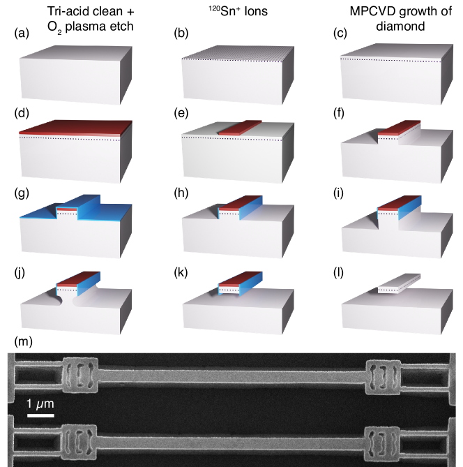
An electronic grade diamond chip from ElementSix is first cleaned in a boiling tri-acid solution consisting of nitric, sulfuric, and perchloric acids in equal part. The top nm of the diamond chip is then removed via an oxygen (O2) plasma etch (Figure 1(a)). The subsequent color center generation and nanofabrication steps are detailed below and illustrated schematically in Figure 1.
SnV- centers are generated on the chip via the shallow ion implantation and growth (SIIG) method25. The prepared chip is implanted by CuttingEdge Ions with 120Sn+ ions at 1 keV and a dose of cm-2 (Figure 1(b)). The implanted chip is then cleaned with a hydrogen (H2) plasma immediately before 90 nm of diamond is grown via microwave-plasma chemical vapor deposition (MPCVD, Seki Diamond Systems SDS 5010) as detailed in Ref. 25 and shown in Figure 1(c).
With SnV- centers embedded 90 nm below the diamond surface, we fabricate suspended bare waveguides. We first grow 200 nm of SixNy via plasma-enhanced chemical vapor deposition (PECVD) to serve as an etch mask (Figure 1(d)). We define the structures in hydrogen silsesquioxane FOx-16 via electron-beam lithography and transfer the pattern into the SixNy with a SF6, CH4, and N2 reactive ion etch (RIE) (Figure 1(e)). With the SixNy etch mask patterned, we then etch the diamond with an anisotropic O2 RIE (Figure 1(f)). Next, 30 nm of Al2O3 are grown via atomic layer deposition (Figure 1(g)). The horizontal planes of the Al2O3 layer are removed with a Cl2, BCl2, and N2 RIE (Figure 1(h)). A second anisotropic O2 RIE is performed to expose part of the vertical sidewalls of the diamond structure (Figure 1(i)). The quasi-isotropic etch26, 27, 28, 29 step can now be performed to undercut the structures (Figure 1(j)). To do so, the forward bias of the O2 RIE is turned off, and the etch is performed at high temperature with high inductively coupled plasma power26, 27, 28, 29. The resulting etch progresses preferentially along the {110} planes26. When the nanobeam waveguides have been released (Figure 1(k)) and have been etched to the desired thickness, as validated by high-voltage scanning electron microscopy (SEM) imaging, the sample is soaked in hydrofluoric acid to remove the SixNy and Al2O3 etch masks (Figure 1(l)).
The resulting waveguides are 400 nm wide, 10 m long, and 280 nm thick. On either end of the waveguides is an inverse-designed31, 29 vertical coupler (VC) to couple incident light from free space into the waveguide and vice versa. A SEM image of a typical resulting nanostructure is shown in Figure 1(m). We successfully fabricated more than 1000 waveguide structures across our 2 2 mm2 chip.

3 Results and discussion
3.1 Photoluminescence map
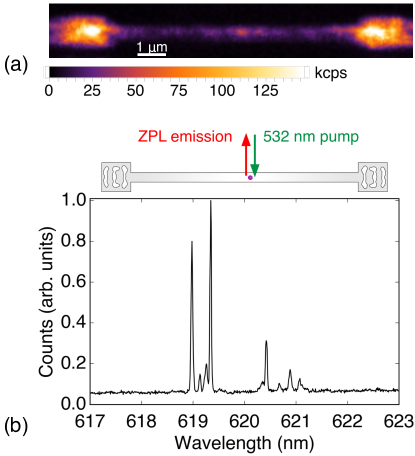
To characterize the fabricated devices, we use two home-built cryogenic setups. First, we acquire two-dimensional photoluminescence (PL) maps of potential structures using a scanning confocal microscope operating at 5 K. In this setup, an objective lens inside the cryostat (Montana Instruments) focuses a continuous-wave laser at 532 nm on the sample to excite the emitters non-resonantly. The emitted photons are collected using the same objective lens and a single-mode fiber. We spectrally filter the collected light using a 568-nm long-pass filter and send the filtered signal to a single-photon counting module. A typical resulting PL map of a nanobeam waveguide on this sample is shown in Figure 2(a). The high counts and distinct bright spots apparent on the device in the PL map indicate the existence of SnV- centers in the nanobeam. PL spectroscopy is next used to confirm the presence of SnV- centers in the devices.

3.2 Photoluminescence excitation
To characterize the linewidth of the emitters, we move to another cryostat (attoDRY2100) that operates at 1.7 K. We first collect a PL spectrum, shown in Figure 2(b) by focusing a 532-nm laser on a spot in the middle of the waveguide, collecting the emitted light from the same spot with a multimode fiber, and sending the collected light to a spectrometer. This spectrum displays multiple distinct zero-phonon lines clustered around the expected wavelengths of the C and D transitions9 of the SnV- center, indicating that multiple SnV- centers are present in the nanobeam waveguide. In the Supporting Information32, we inspect several other waveguides and confirm the presence of SnV- centers in all of the studied structures.
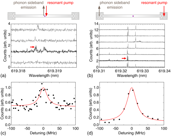
We perform photoluminescence excitation (PLE) on the C transition of a color center in the same waveguide. We scan the wavelength of the MSquared External Mixing Module around the resonant wavelength of the color center of interest. Counting photons emitted into the phonon sideband of the SnV- center, we observe a peak in emission as the laser crosses resonance with the color center and thus can infer the linewidth of the color center. We perform PLE in two configurations: top-down and VC-to-VC. In the former, illustrated schematically in Figure 3(a), the excitation laser is coupled out of a single-mode polarization maintaining fiber and is focused on a spot on the waveguide. The collection fiber is aligned to the same spot on the waveguide. In the VC-to-VC configuration, illustrated schematically in Figure 3(b), the excitation spot is focused on one VC. The emission is collected from the opposite VC. In both configurations, the emitted light is passed through a 638-nm long-pass filter and a 700-nm short-pass filter before being collected by a multimode fiber.
3.2.1 Narrow-linewidth SnV- centers in waveguides
Figures 3(a) and (b) display the resulting PLE data for the top-down and VC-to-VC configurations respectively. The different passes of the laser through resonance are offset in the plot for clarity, with the lowest scan being the first. The many peaks in Figure 3(b) may indicate that several emitters are coupled to the waveguide, as expected from the PL shown in Figure 2.
From the data in Figures 3(a) and (b), we fit a Lorentzian to one peak for each configuration, indicated by a red arrow. The Lorentzian fits to these data, shown in Figures 3(c) and (d), reveal linewidths of MHz and MHz respectively. Notably, both of these linewidths are comparable to previously reported lifetime-limited linewidths13, 30 despite the several fabrication steps performed on this sample. The narrow linewidths of the SnV- centers presented in Figure 3 are reproducible in other SnV- centers. PLE and linewidth data of several additional SnV- centers are provided in the Supporting Information 32. The average linewidth of these other SnV- centers is MHz. The ability to produce narrow-linewidth SnV- centers in suspended waveguides will enable the future fabrication of large-scale photonic circuitry and quantum photonics experiments.

3.2.2 Blinking and spectral diffusion
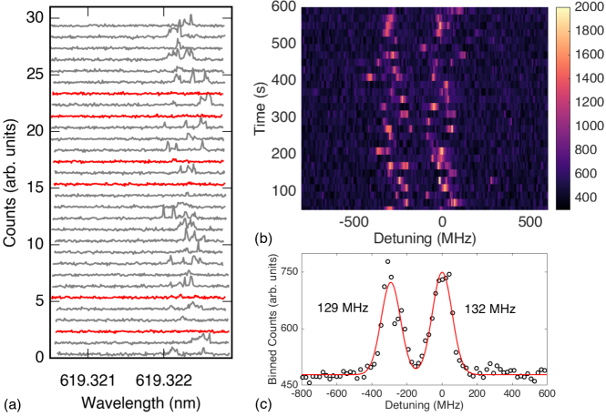
In both configurations, Figures 3(a) and (b), multiple peaks are apparent in several scans but not all appear in the same scans. The inconsistent appearances of some peaks, known as blinking, may indicate instabilities in the charge states of those emitters30. We also observe that the lines vary slightly in frequency between PLE scans, or display spectral diffusion. The fact that these instabilities are observed in both configurations confirms that this is a color-center-related phenomenon rather than a waveguide-related one. Similar observations have been reported in Ref. 30 where SnV- centers were generated via high-energy ion implantation and HPHT annealing.
In Figure 4(a), we highlight in red the PLE scans in which the SnV- center under study blinked. In a survey of SnV- centers in waveguides, we found that seven of the nine SnV- centers that we studied blinked at least once during ten minutes of consecutive PLE scans. Additional details on the quantitative definition of blinking and the dependence of blinking on excitation power can be found in the Supporting Information 32.
Figures 4(b) and (c) show an example of the analysis of the spectral diffusion of SnV- centers in a waveguide. Consecutive PLE scans are acquired for ten minutes (Figure 4(b)). The data are then binned in frequency to form a histogram of counts at different frequencies, as shown in Figure 4(c). Because of the random nature of the spectral diffusion, we fit a Gaussian to the histogram. We quantify the spectral diffusion by calculating the full width at half maximum of the fit. In Figures 4(b) and (c), the distribution is bimodal with full widths at half maximum of about 130 MHz. A statistical study of the spectral diffusion of several SnV- centers and data on the power dependence of spectral diffusion are provided in the Supporting Information 32.

4 Conclusion and outlook
In this work we have integrated narrow-linewidth SnV- centers in diamond nanobeam waveguides. These results indicate that the combination of the SIIG method25 and the quasi-isotropic undercut26, 27, 28, 29 forms a promising platform for future quantum photonics with the SnV- center. For example, carefully optimizing the coupling efficiency of the narrow-linewidth emitter to the waveguide mode enables a broadband interface for spin-controlled photon switching33 and few-photon nonlinearity34. We have also investigated the spectral diffusion and blinking of the waveguide-coupled SnV- centers. Electromechanically controlled waveguides may increase the stability of emitters by reducing the charge and strain related noise35. However, further experimental efforts are required to understand and to mitigate the source of instability in the emission spectra of the SnV- centers.
To go beyond single-emitter experiments, deterministic positioning of the SnV- centers along the waveguide is essential. Fortunately, as previously demostrated in Ref. 25, we can achieve site-controlled generation of SnV- centers with an implantation mask defined with standard lithography. Deterministic positioning combined with small inhomogeneous broadening of SnV- centers will enable the coupling of multiple identical emitters to the same optical mode for superradiance and quantum few-body experiments23, 24, 36.
Moreover, having high-quality SnV- centers in suspended nanophotonic structures in diamond enables the future integration of the color centers into cavities to enhance the spin-photon interaction. Ultimately, such devices will be beneficial for several quantum information applications and can operate at elevated temperatures compared to previous demonstrations with SiV- centers19.
This work is financially supported by Army Research Office (ARO) (award no. W911NF-13-1-0309); National Science Foundation (NSF) RAISE TAQS (award no. 1838976); Air Force Office of Scientific Research (AFOSR) DURIP (award no. FA9550-16-1-0223); Department of Energy, Basic Energy Sciences (BES) - Materials Science and Engineering (award no. DE-SC0020115). SIMES work is supported by the DOE Office of Sciences, Division of Materials Science and Engineering; and SLAC LDRD. A.E.R. acknowledges support from the National Defense Science and Engineering Graduate (NDSEG) Fellowship Program, sponsored by the Air Force Research Laboratory (AFRL), the Office of Naval Research (ONR) and the Army Research Office (ARO). C.D. acknowledges support from the Andreas Bechtolsheim Stanford Graduate Fellowship and the Microsoft Research PhD Fellowship. S.A. acknowledges support from Bloch postdoctoral fellowship in quantum science and engineering from Stanford Q-FARM. Part of this work was performed at the Stanford Nanofabrication Facility (SNF) and the Stanford Nano Shared Facilities (SNSF), supported by the National Science Foundation under award ECCS-1542152.
References
- Kimble 2008 Kimble, H. J. The quantum internet. Nature 2008, 453, 1023–1030
- Awschalom et al. 2018 Awschalom, D. D.; Hanson, R.; Wrachtrup, J.; Zhou, B. B. Quantum technologies with optically interfaced solid-state spins. Nat. Photon. 2018, 12, 516–27
- Neu et al. 2011 Neu, E.; Steinmetz, D.; Riedrich-Möller, J.; Gsell, S.; Fischer, M.; Schreck, M.; Becher, C. Single photon emission from silicon-vacancy colour centres in chemical vapour deposition nano-diamonds on iridium. New J. Phys. 2011, 13, 025012
- Hepp et al. 2014 Hepp, C.; Müller, T.; Waselowski, V.; Becker, J. N.; Pingault, B.; Sternschulte, H.; Steinmüller-Nethl, D.; Gali, A.; Maze, J. R.; Atatüre, M.; Becher, C. Electronic Structure of the Silicon Vacancy Color Center in Diamond. Phys. Rev. Lett. 2014, 112, 036405
- Müller et al. 2014 Müller, T.; Hepp, C.; Pingault, B.; Neu, E.; Gsell, S.; Schreck, M.; Sternschulte, H.; Steinmüller-Nethl, D.; Becher, C.; Atatüre, M. Optical signatures of silicon-vacancy spins in diamond. Nat. Commun. 2014, 5, 3328
- Iwasaki et al. 2015 Iwasaki, T. et al. Germanium-Vacancy Single Color Centers in Diamond. Sci. Rep. 2015, 5, 12882
- Palyanov et al. 2015 Palyanov, Y. N.; Kupriyanov, I. N.; Borzdov, Y. M.; Surovtsev, N. V. Germanium: a new catalyst for diamond synthesis and a new optically active impurity in diamond. Sci. Rep. 2015, 5, 14789
- Ekimov et al. 2015 Ekimov, E. A.; Lyapin, S. G.; Boldyrev, K. N.; Kondrin, M. V.; Khmelnitskiy, R.; Gavva, V. A.; Kotereva, T. V.; Popova, M. N. Germanium–Vacancy Color Center in Isotopically Enriched Diamonds Synthesized at High Pressures. JETP Lett. 2015, 102, 701–706
- Iwasaki et al. 2017 Iwasaki, T.; Miyamoto, Y.; Taniguchi, T.; Siyushev, P.; Metsch, M. H.; Jelezko, F.; Hatano, M. Tin-Vacancy Quantum Emitters in Diamond. Phys. Rev. Lett. 2017, 119, 253601
- Tchernij et al. 2017 Tchernij, S. D.; Herzig, T.; Forneris, J.; Küpper, J.; Pezzagna, S.; Train, P.; Morev, E.; Brida, I. P. D. G.; Skukan, N.; Genovese, M.; Jakšić, M.; Meijer, J.; Olivero, P. Single-Photon-Emitting Optical Centers in Diamond Fabricated upon Sn Implantation. ACS Photonics 2017, 4, 2580–6
- Ekimov et al. 2018 Ekimov, E. A.; Lyapin, S. G.; Kondrin, M. V. Tin-vacancy color centers in micro- and polycrystalline diamonds synthesized at high pressures. Diam. Relat. Mater. 2018, 87, 223–7
- Rugar et al. 2019 Rugar, A. E.; Dory, C.; Sun, S.; Vučković, J. Characterization of optical and spin properties of single tin-vacancy centers in diamond nanopillars. Phys. Rev. B 2019, 99, 205417
- Trusheim et al. 2020 Trusheim, M. E. et al. Transform-Limited Photons From a Coherent Tin-Vacancy Spin in Diamond. Phys. Rev. Lett. 2020, 124, 023602
- Trusheim et al. 2019 Trusheim, M. E.; Wan, N. H.; Chen, K. C.; Ciccarino, C. J.; Flick, J.; Sundararaman, R.; Malladi, G.; Bersin, E.; Walsh, M.; Lienhard, B.; Bakhru, H.; Narang, P.; Englund, D. Lead-related quantum emitters in diamond. Phys. Rev. B 2019, 99, 075430
- Tchernij et al. 2018 Tchernij, S. D. et al. Single-Photon Emitters in Lead-Implanted Single-Crystal Diamond. ACS Photonics 2018, 5, 4864–71
- Evans et al. 2016 Evans, R. E.; Sipahigil, A.; Sukachev, D. D.; Zibrov, A. S.; Lukin, M. D. Narrow-Linewidth Homogeneous Optical Emitters in Diamond Nanostructures via Silicon Ion Implantation. Phys. Rev. Applied 2016, 5, 044010
- Bradac et al. 2019 Bradac, C.; Gao, W.; Forneris, J.; Trusheim, M.; Aharonovich, I. Quantum nanophotonics with group IV defects in diamond. Nat. Commun. 2019, 10, 5625
- Nguyen et al. 2019 Nguyen, C. T.; Sukachev, D. D.; Bhaskar, M. K.; Machielse, B.; Levonian, D. S.; Knall, E. N.; Stroganov, P.; Riedinger, R.; Park, H.; Lončar, M.; Lukin, M. D. Quantum Network Nodes Based on Diamond Qubits with an Efficient Nanophotonic Interface. Phys. Rev. Lett. 2019, 123, 183602
- Bhaskar et al. 2020 Bhaskar, M. K.; Riedinger, R.; Machielse, B.; Levonian, D. S.; Nguyen, C. T.; Knall, E. N.; Park, H.; Englund, D.; Lončar, M.; Sukachev, D. D.; Lukin, M. D. Experimental demonstration of memory-enhanced quantum communication. Nature 2020, 580, 60–64
- Bhaskar et al. 2017 Bhaskar, M. K.; Sukachev, D. D.; Sipahigil, A.; Evans, R. E.; Burek, M. J.; Nguyen, C. T.; Rogers, L. J.; Siyushev, P.; Metsch, M. H.; Park, H.; Jelezko, F.; Lončar, M.; Lukin, M. D. Quantum Nonlinear Optics with a Germanium-Vacancy Color Center in a Nanoscale Diamond Waveguide. Phys. Rev. Lett. 2017, 118, 223603
- Bray et al. 2018 Bray, K.; Regan, B.; Trycz, A.; Previdi, R.; Seniutinas, G.; Ganesan, K.; Kianinia, M.; Kim, S.; Aharonovich, I. Single Crystal Diamond Membranes and Photonic Resonators Containing Germanium Vacancy Color Centers. ACS Photonics 2018, 5, 4817–22
- Thiering and Gali 2018 Thiering, G.; Gali, A. Ab Initio Magneto-Optical Spectrum of Group-IV Vacancy Color Centers in Diamond. Phys. Rev. X 2018, 8, 021063
- Sipahigil et al. 2016 Sipahigil, A. et al. An integrated diamond nanophotonics platform for quantum-optical networks. Science 2016, 354, 847–50
- Grim et al. 2019 Grim, J. Q.; Bracker, A. S.; Zalalutdinov, M.; Carter, S. G.; Kozen, A. C.; Kim, M.; Kim, C. S.; Mlack, J. T.; Yakes, M.; Lee, B.; Gammon, D. Scalable in operando strain tuning in nanophotonic waveguides enabling three-quantum-dot superradiance. Nat. Mater. 2019, 18, 963–969
- Rugar et al. 2020 Rugar, A. E.; Lu, H.; Dory, C.; Sun, S.; McQuade, P. J.; Shen, Z.-X.; Melosh, N. A.; Vučković, J. Generation of Tin-Vacancy Centers in Diamond via Shallow Ion Implantation and Subsequent Diamond Overgrowth. Nano Lett. 2020, 20, 1614–1619
- Mouradian et al. 2017 Mouradian, S.; Wan, N. H.; Schröder, T.; Englund, D. Rectangular photonic crystal nanobeam cavities in bulk diamond. Appl. Phys. Lett. 2017, 111, 021103
- Wan et al. 2018 Wan, N. H.; Mouradian, S.; Englund, D. Two-dimensional photonic crystal slab nanocavities on bulk single-crystal diamond. Appl. Phys. Lett. 2018, 112, 141102
- Mitchell et al. 2019 Mitchell, M.; Lake, D. P.; Barclay, P. E. Realizing Q> 300 000 in diamond microdisks for optomechanics via etch optimization. APL Photonics 2019, 4, 016101
- Dory et al. 2019 Dory, C.; Vercruysse, D.; Yang, K. Y.; Sapra, N. V.; Rugar, A. E.; Sun, S.; Lukin, D. M.; Piggott, A. Y.; Zhang, J. L.; Radulaski, M.; Lagoudakis, K. G.; Su, L.; Vučković, J. Inverse-designed diamond photonics. Nat. Commun. 2019, 10, 3309
- Görlitz et al. 2020 Görlitz, J.; Herrmann, D.; Thiering, G.; Fuchs, P.; Gandil, M.; Iwasaki, T.; Taniguchi, T.; Kieschnick, M.; Meijer, J.; Hatano, M.; Gali, A.; Becher, C. Spectroscopic investigations of negatively charged tin-vacancy centres in diamond. New J. Phys. 2020, 22, 013048
- Molesky et al. 2018 Molesky, S.; Lin, Z.; Piggott, A. Y.; Jin, W.; Vučković, J.; Rodriguez, A. W. Inverse design in nanophotonics. Nat. Photon. 2018, 12, 659–670
- 32 See Supporting Information.
- Javadi et al. 2018 Javadi, A. et al. Spin–photon interface and spin-controlled photon switching in a nanobeam waveguide. Nat. Nanotechnol. 2018, 13, 398–403
- Thyrrestrup et al. 2018 Thyrrestrup, H. et al. Quantum Optics with Near-Lifetime-Limited Quantum-Dot Transitions in a Nanophotonic Waveguide. Nano Lett. 2018, 18, 1801–1806
- Machielse et al. 2019 Machielse, B. et al. Quantum Interference of Electromechanically Stabilized Emitters in Nanophotonic Devices. Phys. Rev. X 2019, 9, 031022
- Kim et al. 2018 Kim, J.-H.; Aghaeimeibodi, S.; Richardson, C. J. K.; Leavitt, R. P.; Waks, E. Super-Radiant Emission from Quantum Dots in a Nanophotonic Waveguide. Nano Lett. 2018, 18, 4734