font=small
![[Uncaptioned image]](/html/2005.09044/assets/toc.png)
On the dopability of semiconductors and governing materials properties
Abstract
To be practical, semiconductors need to be doped. Sometimes, to nearly degenerate levels, e.g. in applications such as thermoelectric, transparent electronics or power electronics. However, many materials with finite band gaps are not dopable at all, while many others exhibit strong preference toward allowing either - or -type doping, but not both. In this work, we develop a model description of semiconductor dopability and formulate design principles in terms of governing materials properties. Our approach, which builds upon the semiconductor defect theory applied to a suitably devised (tight-binding) model system, reveals analytic relationships between intrinsic materials properties and the semiconductor dopability, and elucidates the role and the insufficiency of previously suggested descriptors such as the absolute band edge positions. We validate our model against a number of classic binary semiconductors and discuss its extension to more complex chemistries and the utility in large-scale material searches.
1 Introduction
The ability of classic semiconductors such as Si, GaAs, and PbTe to be doped both - and -type and to nearly arbitrary charge carrier concentrations is an exception rather than a rule. This is clearly illustrated by our literature survey, depicted in Fig. 1. We collected the highest measured charge carrier concentrations for about 130 binary and ternary semiconductors. A number of these compounds have relatively low (maximal) reported charge carrier concentrations and only a small fraction (36 out of 130) have been successfully doped both - and -type. These numbers decrease significantly as the material band gap increases such that there are very few wide-gap semiconductors that are dopable at all (13 out of 130 with gaps above 3 eV), with GaN being the only (weakly) ambipolar semiconductor with the band gap exceeding 3 eV. Recent predictions offer some hope that ambipolar wide-gap materials could exist, though experimental validation is still needed 1, 2, 3. Majority (95 out of 130) of the compounds from Fig. 1 likely suffer from the so-called doping asymmetry, meaning that they can be doped either - or -type, but not both.
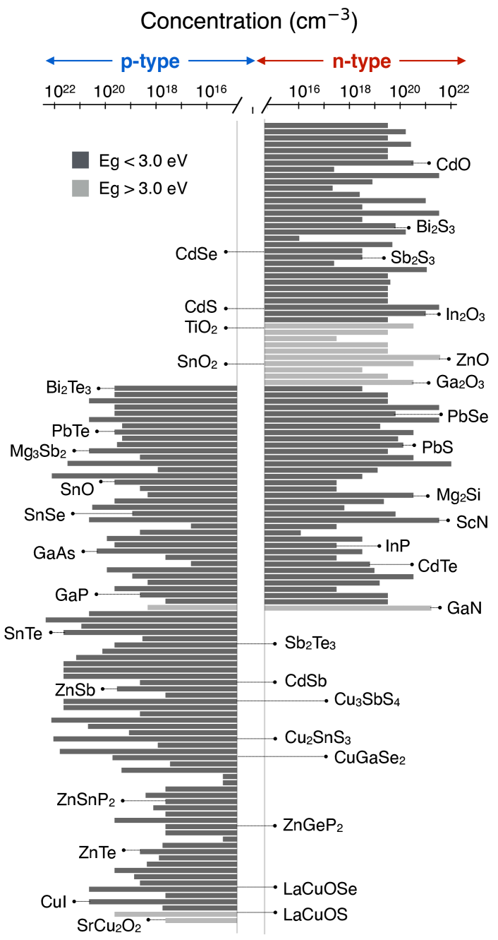
GaN is a notable example of how finding ways to overcome these doping tendencies (or bottlenecks) can be transformative. A nominally exclusively -type semiconductor was successfully doped -type via a rather unconventional non-equilibrium processing route that allows insertion of acceptor behaving Mg substitutional impurities in much higher concentrations than possible under equilibrium conditions. This accomplishment enabled the development of a blue light emitting diode which was awarded 2014 Nobel prize in physics 79, 80, 81. Likewise, numerous attempts have been made to dope ZnO, SnO2, and In2O3 -type 82, 83, 84; however, with very little success, and to this day, these compounds are regarded as exclusively -type semiconductors 85, 86. Recent predictions suggest that the -type doping in ZnO could be attained; however, not in the ground state wurtzite structure but in the metastable, high-pressure rocksalt phase 87. Another important (counter) example is Mg3Sb2, which was for long regarded as an exclusively -type semiconductor, a belief that was recently contested by the successful (equilibrium) -doping followed by the demonstration of high thermoelectric performance in the -type Mg3Sb2 88, 89. These doping tendencies and bottlenecks represent a critical obstacle for the discovery and design of novel functional materials; especially for applications such as thermoelectric, transparent, and power electronics where achieveing nearly degenerate charge carrier concentrations is of utmost importance 90, 91, 92.
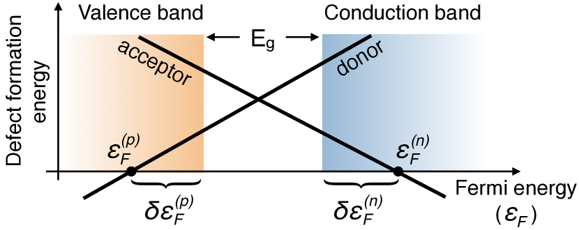
Dopability of III-V and II-VI semiconductors was investigated previously. Zunger formulated his practical doping principles as related to the formation of intrinsic compensating defects 93. Namely, the formation energy of any acceptor defect exhibits decreasing linear dependence on the Fermi energy () while for the donors it increases linearly with as shown in Fig. 2. Hence, there will be a special value above which the energy to form intrinsic acceptors becomes negative (exothermic). Similarly, there is a special below which the formation of intrinsic donors will be exothermic. As a consequence, any attempt to dope the system -type by increasing beyond the will be met with the opposition in the form of spontaneous formation of intrinsic acceptor (electron-compensating) defects. If occurs near or inside the conduction band, the system will allow introduction of electrons and hence, represents a natural upper limit for -type doping. Analogously, intrinsic donors and the resulting determine the limit for -type doping.
What Zunger noticed is that within III-V and II-VI semiconductors the - and -type pinning energies and , as he called them, obtained from defect calculations approximately align. This implies that in order to be dopable, the semiconductor band edges need to be close to these “universal" pining energies. That is, lower the CBM position relative to the -pinning energy, the more -type dopable the systems is, and conversely, higher the VBM relative to the -pinning energy, the more -type dopable the semiconductor. While certainly practical, Zunger’s doping principles critically rely on the empirically observed alignment of the doping pinning energies, which, as we will show later, does not hold generally for compounds outside III-V and II-VI semiconductors.
Similar design principles emerge from the consideration of another “universal” reference, the branch point energy 94. It is defined as the energy at which the electronic states at the surface and/or interfaces change their character from predominantly VB-like to mostly CB-like, and is also used implicitly to define dopability as related to the proximity of the band edges. Lower the CBM relative to branch point energy, more -type dopable the system is; and higher the VBM, more -type dopable the system is. If the branch point energy occurs close to the mid-gap, the system could be either ambipolar dopable or insulating. The expected universal alignment of the branch point energies between different materials then implies dopability design principles in terms of the positions of the band edges similar to those proposed by Zunger, but now relative to this different reference. However, recent work shows that considerations based on the branch point energy can be used to identify -type dopable systems much better than the ambipolar or the -type systems 95.
Also recently, Miller et al. used machine learning to develop an empirical model for dopability in diamond-like semiconductors 7. While the developed model shows remarkable accuracy in reproducing and predicting achievable carrier concentrations, as with any machine learning model its relation to the underlying physics is unclear (not causal) and the transferability beyond the diamond-like semiconductors is questionable due to the scarcity of measured carrier concentrations needed for the model development.
Herein, we revisit the problem of predicting dopability of semiconductors and build upon these previous works. We ask the question of the complete set of governing intrinsic material properties and the causal relationship between them, without making the largely qualitative and heuristic assumptions about the alignment of the pinning energies or the connection of dopability to the branch point energy. We do this by formulating a model description of a binary ionic semiconductor using the tight-binding model for non-interacting electrons supplemented by the nucleus-nucleus repulsion (pair) potential. We use this model to derive analytic expressions for the formation energy of intrinsic donors and acceptors and the associated doping pinning energies. The model is validated against directly calculated (first-principles) pinning energies. Finally, we analyze the new insights that are provided by the model, the role of previous heuristics as well as its utility in searching for dopable materials. It is important to note however, that modern defect theory and defect calculations 96, 97 can be used to predict both intrinsic limits to dopability (doping pinning energies) and the effectiveness of extrinsic dopants 89, 98. The aim here is to uncover physical principles of semiconductor dopability that are usually implicit and hidden in numerical approaches.
2 Dopability model
2.1 Construction
Let’s consider a binary C1A1 ionic semiconductor defined as follows:
-
(i)
it is composed of two kinds of atoms A and C, one more electronegative taking a role of an anion (A) and the other less electronegative (cation-C),
-
(ii)
every anion (cation) contributes () number of atomic orbitals and () number of electrons where the charge balance between the cations and anions implies ,
-
(iii)
electrons interact only with the nuclei and not among themselves (independent electron approximation),
-
(iv)
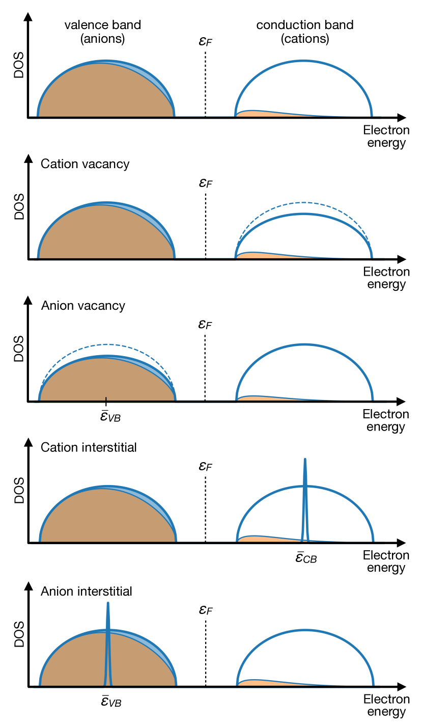
band gap forms between two bands, the valence band that is predominantly of the anion character and the cation derived conduction band (Fig. 3 topmost panel),
-
(v)
defects such as anion or cation vacancies only affect the valence band (anion defects) or conduction band (cation defects) densities of states, while interstitial defects add atomic orbitals with the energy that falls in the middle of the corresponding band (Fig. 3 lower panels), and
-
(vi)
we also neglect any changes to the density of states that are due to relaxations of atomic positions upon defect formation.
For the sake of simplicity, we have intentionally neglected the possibility of vacancy states occurring deep inside the band gap. This is not a big limitation as the deep donors are typically fully ionized close to the top valence band, as are deep acceptors close to the bottom of the conduction band. Under these circumstances the above assumptions should still apply. To describe this (idealized) binary system, we will utilize a model Hamiltonian with electrons described within the tight-binding approximation and the repulsion between nuclei through the pair potential term 99. For our discussion it is more useful to write the total energy of the system:
| (1) |
where the summation in the first term goes over all occupied electronic states as determined by the Fermi-Dirac distribution function , and the second term is the nuclear repulsion term. Note that this expression is only valid if the electron-electron interactions are neglected.
2.2 Defect formation energies
As already discussed, the intrinsic aspects of semiconductor dopability can be formulated in terms of the energy to form intrinsic compensating defects that prevent (compensate) introduction of free charge carriers of the desired type ( or ). The energy to form a single point defect is given as:
| (2) |
where and represent the energy of the system with and without the defect , respectively; while is the chemical potential of the respective chemical reservoirs with which the exchange of atoms occurs upon forming the defect. The plus sign in corresponds to vacancies while the minus is used in case of interstitials.
Cation vacancy. Within the above model, formation of a cation vacancy will result in: (i) absence of a nucleus at a particular cation site , (ii) removal of the number of electrons from the system, and (iii) reduction of the density of states primarily in the conduction band in the amount equal to the number of states each cation contributes to the system. As illustrated in Fig. 3, we will assume that this reduction in the number of conduction band states is distributed in a way that does not affect the average energy of conduction band while the overall number of states is reduced by . It is also important to note that the Fermi statistics in combination with the largely unchanged DOS in the valence band implies that the number of holes created by removing one cation will thermalize over both valence and conduction bands and will have the energy equal to the negative electron chemical potential or the Fermi energy () as illustrated in Fig. 3. By incorporating these considerations into equations (1) and (2) the energy to form one cation vacancy () becomes:
| (3) |
where the first term on the righthand side represents the energy contribution due to the difference in occupation of the electronic states between the defect and host system ( holes with energy ), the second term represents the energy difference in the nuclear repulsion due to the missing cation at the site (nuclear repulsion potential of that site), and as before, the last term represents the cation chemical potential. In the derivation of eq. (3) we also assumed that creating a cation vacancy does not appreciably affect the Fermi energy, i.e., the of the defect system equals that of the host. Rigorously, this assumption is valid in the case of low vacancy concentration (the dilute limit). Given the chemical composition and the crystal structure, which set the and the some value of the cation chemical potential set by the state of the cation reservoir, the becomes the decreasing function of the Fermi energy as in depicted in Fig. 2.
As usually done in defect calculations 97, 96, one can further separate the total chemical potential into that of the standard cation phase at standard conditions (), i.e., that of the solid metal at room temperature and ambient pressure, and the deviation from the reference value (). Applying the same model Hamiltonian and the total energy formula from eq. (1) one can write the reference chemical potential as , where represents a characteristic (average) energy of an electron in the reference phase while stands for the average nuclear repulsion energy (per nucleus). While we will keep as a separate entity, it is worthwhile noting that one can think of as approximately at the same energy as the center of the conduction band. After implementing these equations for the chemical potential the formation energy of the cation vacancy becomes:
| (4) |
This equation provides a relatively simple physical picture of the cation vacancy formation, which involves transfer of electrons from the system into the reference phase quantified by the energy of that transfer (first parenthesis) and transfer of a cation nucleus from the system into the reference phase quantified by the difference in the nuclear repulsion (second parentheses). The last term describes the deviation of the actual cation reservoir from the standard state and is a function of the parameters such as temperature and pressure. Lastly, it is important to note that and need to be expressed relative to the common reference, which is usually assumed to be the vacuum level. Please note that Varley et al.100 recently showed that for the tetrahedrally bonded semiconductors the cation vacancy formation energy can be correlated to the branch point energy.
Anion vacancy. Analogously, in our model the creation of an anion vacancy will result in: (i) the absence of a nucleus at a particular anion site (let’s label it again), (ii) removal of the number of electrons from the system, and (iii) reduction of the density of states primarily in the valence band, in the integral amount equal to the number of states each anion contributes to the system. One can derive an equation for the formation energy of an anion vacancy similar to eq. (4) with one key difference. Now, the reduction in the number of valence band states needs to be taken into account. The easiest way is to see how to include the reduction in the valence band DOS is to assume low temperature relative to the band gap so that all valence band states are approximately fully occupied. If this is the case then the difference in the summation over all occupied states will amount to the number of states that are missing () times the average energy of the valence band states (). Also, the electrons that were previously occupying the missing states in the valence band will now be thermalized across the band gap giving rise to the term. Taking all these contributions into account the anion vacancy formation energy is given as:
| (5) |
After applying the already described procedure for , and noting that the anion vacancy formation energy becomes:
| (6) | |||||
where, as before, represents some characteristic electronic energy of the anion reference phase (close to the center of the valence band), and stands for its average nuclear repulsion. Hence, the formation of an anion vacancy requires energy which is an increasing function of and involves transfer of the cation electrons () from the valence band to the , transfer of the anion electrons () from the valence band into the anion reference phase, transfer of the anion nucleus from the system into the anion reference phase, and, as before, the last term describes the deviation of the actual anion reservoir from the standard state.
Interstitial defects. To first order the interstitial defects, either the cation or the anion ones, can be approximated as contributing their atomic orbitals and their valence electrons to the system. The cation interstitial will contribute the number of localized states at approximately the mid-conduction band energy and the number of electrons that would follow the Fermi-Dirac distribution and distribute themselves within the valence and the conduction bands so that their average energy in the dilute limit will become as illustrated in Fig. 3. The anion interstitial on the other hand, contributes partially filled orbitals with electrons at the mid-valence band. Because of the charge transfer to fill these states there will be holes created having the energy . The formation of these two defects requires the energy that can be derived in a similar fashion like previous two amounting to:
| (7) | |||||
where and stand for the formation energy of the cation and anion interstitial defects, respectively, occupying lattice sites that are labeled in both cases.
2.3 Dopability metrics and the emerging design principles
The relevance of the previous derivations to the question of dopability, the very topic of this paper, follows from the Zunger’s formulation of dopability 93 in terms of the intrinsic compensating defects and the corresponding doping pinning energies and , as already described (see Fig. 2). The usual culprits preventing (compensating) the introduction of electrons into the conduction band are intrinsic acceptor defects such as the cation vacancies and/or anion interstitials, while the anion vacancies and cation interstitials typically obstruct -type doping. Having this in mind the expressions for and , in Fig. 2, can be defined as:
| (8) |
where the -type doping limit is the minimal doping pinning energy among all the intrinsic acceptor defects, while the -type doping limit is the maximal doping pinning energy among all the intrinsic donors.
To simplify the discussion we will focus on vacancies because in binary systems they are most often the doping limiting defects, and will discuss how the main results changes in case interstitial defects are the limiting factor. Also, to make the expressions easier for discussion, we will express pinning energies relative to the corresponding band edge as and as shown in Fig. 2. Under the assumption that vacancies determine the dopability of materials, and can be derived from the condition that the formation energy of the corresponding defect equals to zero at the pinning energies. From equations (4) and (6) one finds:
| (9) | |||||
| Term | Description | Quantity or Proxy used in validation (symbol) |
|---|---|---|
| average electronic energy in cation reference phase | work function of cation reference phase () | |
| average electronic energy in anion reference phase | work function of anion reference phase () | |
| difference in nuclear repulsion between cation | compound’s enthalpy of formation () | |
| reference phase and site in the compound | ||
| difference in nuclear repulsion between anion | compound’s enthalpy of formation () | |
| reference phase and site in the compound | ||
| average energy of valence band states | calculated from density of states | |
| average energy of cation -states | calculated from density of states | |
| conduction band minimum | GW calculated absolute | |
| valence band maximum | GW calculated absolute |
Within this model the and effectively become - and - dopability metrics. The condition for ambipolar dopability requires both pinning energies to be deep inside the corresponding band, which then translates into requiring both and to be positive and large. The following design principles emerge from these requirements.
Design principles for n-type dopability limited by the cation vacancies. First, the CBM of the material needs to be as low as possible, however, not relative to some global reference such as the universal pining energy or the branch point energy, but relative to the characteristic electronic energy of the cation reservoir so to maximize the term. If one thinks of as close in energy to the center of the conduction band then maximization of the first term implies large conduction bandwidth. Second, to make large and positive the nuclear repulsion in the cation reservoir needs to be larger than that in the compound and if this is the case one wants to be small (cation valency). Inversely, if the -type dopability would require to be large so to minimize the harmful influence of this term. However, to accurately assess the influence of this term one needs to know the actual pair potential for a particular system. We will come back to this question later.
Design principles for p-type dopability limited by the anion vacancies. Maximization of the implies qualitatively different requirements. Maximizing the first term demands the VBM to be above the mean valence band energy (). This is always true, but this term is large only in systems with large valence bandwidths. Alternatively, one could imagine increasing by having additional valence bands located above the anion band. While not captured by the original model, this will be discussed later in the text. The second term is likely very small because, to first order, one can think that . Much like before, one would like to have large or small depending on the sign of the energy difference. The third term is analogous to the one for -dopability and demands the nuclear repulsion to be higher in the anion reservoir than in the actual system weighed by the term.
The meaning of the is the same for both - and -dopability. Since , it is desired to have synthesis conditions to be as close to as possible. In other words, one wants to be as rich in the corresponding element as possible to prevent the formation of its vacancies. In binary systems is typically a boundary of the stability region both for cations and anions. We will therefore assume in the reminder of this paper that condition can always be fulfilled. For the purpose of comparing the model with the explicit defect calculations this is a fair assumption, because term is same in both the cases, and hence, exactly cancels out. However, one needs to be cognizant of the fact that in chemical systems with many competing phases, might not be possible to achieve for all phases and for both cations and anions, and that the term may appear as a limiting factor to dopability. But, even in such scenarios, actual range of , based on phase stability analysis, can be accommodated in the model, to provide reasonable estimates for and .
The design principles change in case of interstitials. Similar analysis (see the supplementary for equations) shows that if the donor behaving cation interstitial is the lowest energy defect close to the VBM, then maximizing -type dopability would require: (i) that the VBM is as high as possible relative to the , and (ii) that nuclear repulsion at the interstitial site is much larger than together with relatively small or in the case the needs to be large. In case of the anion interstitials the -dopability would benefit from: (i) small valence band widths and small band gaps, (ii) anions with low-lying atomic orbitals, and (iii) high nuclear repulsion on the interstitial site.
As evident from this discussion, the dopability of semiconductors does not depend on a single material property and is a product of relatively complex tradeoffs between different properties. Also, as previously noted the interstitial defects are usually higher in energy than vacancies in the simple binary systems considered here. This is particularly true for the anion interstitials due to their ionic sizes requiring large amount of space. This is why in the reminder of the text we will focus on vacancies as dominant dopability limiting factors. Only one compound in our study, Mg2Si, turns out to have its -type dopability limited by the cation (Mg) interstitials, for which we do consider the described interstitial defect model.
3 Validation
Validation of our model is done by comparing how accurately it reproduces numerical values for the dopability metrics, and , which we compute directly using modern defect theory and defect calculations. However, the quantities appearing in eq. (2.3) are not easily accessible causing direct evaluation of the model dopability metrics difficult. This is particularly the case for the average electronic energies of the elemental reservoirs as well as the ionic repulsion terms for both the elemental reservoirs and the material of interest. The approach we adopt here is to find proxies for these hard-to-access quantities instead of trying to calculate them directly. This approach follows the same idea as in our previous work in which we successfully developed models for electronic and heat transport in thermoelectric materials using more accessible proxies instead of hard-to-compute quantities 91. If appropriate physical proxies can be found, a simplified model involving these proxies can be made computationally inexpensive as well as predictive. The price of such an approach, however, is the introduction of free parameters into the model that need to be fit to the existing data. The performance of the model is then assessed by the quality of the fit. The following discussion focuses on the dopability metrics derived assuming vacancies as the lowest energy compensating defects. Dopability metrics based on interstitials defects are also derived in the supplementary information.
-type dopability metric. As shown in eq. (2.3) there are three main contributions to , the electronic term, nuclear repulsive term, and the chemical potential term. The electronic term involves average electronic energy of the cation reference phase (solid metal) and the energy of the conduction band minimum. An intuitive proxy for , that is easily accessible from literature, is the negative work function () of the reference phase. However, the work function of metals if expressed as an energy relative to vacuum (negative value) represents the maximal electronic energy and not an average one. Therefore, to account for the difference between and work function, we consider replacing the first term with the proxy of the form , where and are the fitting constants, is the work function of the metal phase and the conduction band minimum (negative electron affinity) of the semiconductor material (measured or calculated). Both , and are expressed relative to the vacuum.
To account for the nuclear repulsion contribution one could fit the parameters of our tight-binding plus nuclear repulsion Hamiltonian to a set of materials properties such as the equilibrium volume, cohesive energy, bulk modulus, etc. While this would be the most appropriate thing to do, it would need to be done for all materials of interest and all elemental phases which would render the whole process impractical. Among material properties, cohesive energies, volume and bulk modulus are well known to be correlated with each other 101, 102. Hence simply considering cohesive energy as a proxy for the nuclear repulsion contribution for a material could suffice. However, as we are interested in the difference () between the compounds and the elemental phase energies, we chose as a proxy as it already include the difference between the compounds and the elemental phase energies, and replace the nuclear repulsion term with linear dependence on the compounds enthalpy of formation . Admittedly, includes contributions both from electrons and nuclei. The choice is motivated by the physical relation to the nuclear repulsion and, in part, by our previous work in which we discovered the relevance of to the formation energy of oxygen vacancies in metal oxides 103. The -type dopability is evaluated under cation-rich condition such that , because it represents the most favorable thermodynamic condition to dope the semiconductor -type.
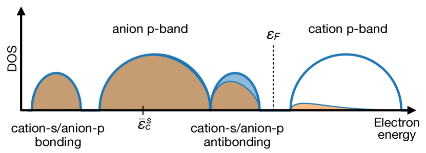
Lastly, to extend the model to systems with partially oxidized cations such as the group-IV and group-V chalcogenides such as SnO, SnS, PbSe, PbTe, Bi2Se3, Bi2Te3, one needs to include an additional term to account for the filled cation -states that contribute to the valence band as shown in Fig. 4. This is easily done by including the transfer of number of the cation -electrons from the valence band to the cation reservoir upon forming the cation vacancy. This term can be written as ) where, is the average electronic energy of the cation reference phase while is the average energy of the cation -states in the material’s valence band (s-DOS center of mass). The latter is obtained from the bulk electronic structure calculations, similar to the average energy of the anion -states in the -type dopability metric. The dopability metric, formulated in terms of the proxies is now given as:
| (10) | |||||
where are the free parameters of the model (fitting constants), that are obtained by fitting to the directly calculated from first-principles defect calculations. The above form also allows extending the model to any CxAy stoichiometry (not only C1A1). The list of terms appearing in the models as well as the corresponding proxies we use for validation is given in Table 1
-type dopability metric. Analogously, terms such as VBM, , and () in the definition of are substituted with the valence band maximum (negative ionization potential) of the semiconductor, negative work function of the anion reference phase or in case of molecules negative first ionization potential (), and the compound’s enthalpy of formation. As discussed earlier, -type dopability metric has an additional term () representing average energy of the valence band, which we evaluate for a set of classic binary semiconductors as the average energy of the anion- states. This is done from the electronic structure calculations (see the methods section) of the bulk, defect-free materials. Finally, the -type dopability is evaluated under anion-rich conditions such that . The dopability metric, formulated in terms of proxies is given as:
| (11) | |||||
where, as before, are free parameters that are fitted to the directly calculated . For each and we have a total of 5 fitting constances which we fit to a set of 16 materials as described further.
The work functions for the cation reference phases, the ionization energies for the gaseous species such as O2, N2 and the enthalpy of formations are obtained from the Refs.104, 105, with details provided in Table S5 of the supplementary information (SI). Compounds’ conduction band minima and valence band maxima (with respect to vacuum) are explicitly calculated using the standard methodology, involving the combination of GW electronic structure and DFT surface calculations 19. Experimental and values are used for Ga2O3 and In2O3. Details of all the above intrinsic material properties of the compounds, along with the average energy of the anion- and cation- states (obtained from calculated DOS) employed in our model are provided in Table S6 of the SI.
We performed defect calculations for a set of 16 binary ionic-semiconductors including classic III-Vs and II-VIs, group-III oxides, and lead and bismuth chalcogenides. Results of the fitting of the and -type dopability metrics eqs. (10) and (11) to the same quantities from defect calculations are shown in Fig 5. We use standard linear regression to obtain values for the fitting parameters. The quality of the fit (as shown in Fig. 5) is very good with the R2=0.91 and 0.81, and root mean square error RMSE=0.26 eV and 0.25 eV for and -type dopability metric, respectively. The final expressions for the two dopability metrics are:
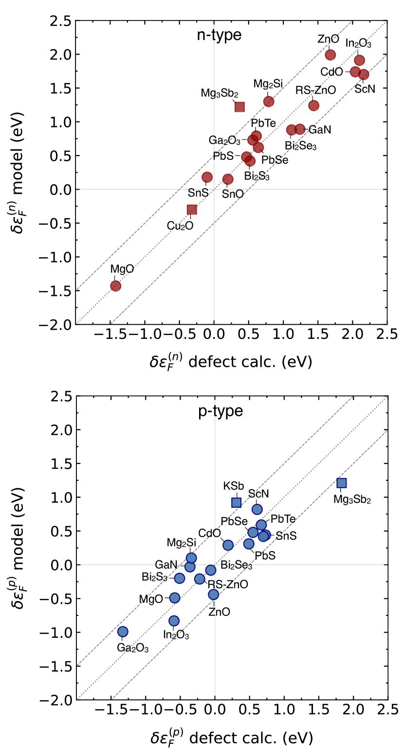
In addition to relying only on the quality of the fit, our model from eq. (3) was further validated against three additional compounds, Mg3Sb2, KSb, Cu2O that were not included in the fitting. As shown in Fig. 5, both - and -type dopability fits very well for Mg3Sb2 because the bonding in Mg3Sb2 satisfies the model assumptions. The -type dopability in KSb fairs well because the valence band is composed of anion (Sb) -states. However, -type dopability for KSb does not agree with the model (not shown), which is not surprising, because the conduction band of KSb does not follow the assumptions of the model, i.e., it is composed of the Sb- orbitals. The original model also does not capture many transition metal compounds which often have contributions of the metal -states to both valence and conduction bands. However, the for systems such as Cu2O where the conduction band is largely composed of Cu- states, our model still works well for the -type dopability as illustrated in Fig. 5. The -type dopability is not well captured because Cu -states contribute heavily to the valence band but not the conduction band106. That said, the model itself can be modified to include these various cases.
It is important to note that all the modeled values of and are within 0.5 eV compared to the values from the defect calculations, which is in our opinion striking given the simplifications and approximations adopted in the model. The magnitude of the coefficients and the contribution of each term in eq. (3) vary with the dopability type. For the -type pinning energy, , individual terms comprising of , and the intercept term, contribute more significantly because they are about an order of magnitude larger than the terms comprising of and . However, for the -type pinning energy, , individual terms comprising and the intercept have an order of magnitude larger coefficients than the , and terms. We will come back to the question of dominant terms in the discussion section. It is also important to note that some of the coefficients turn out to be negative. This is possible because: (i) when substituting physical quantities for proxies we do not know the actual dependencies between the two, (ii) by using the work functions we are using maximal electronic energy of the elemental reservoirs rather than the average one, and lastly, (iii) we are folding into the fitting coefficients both the dependence on the actual stoichiometry and number of valence electrons of cations and anions which could also alter the signs of the coefficients. By doing so we are trying to develop a model that is simple to use. Obviously, the choices we made are not unique and one could in principle come up with the different set of proxies and a different numerical model.
4 Discussion
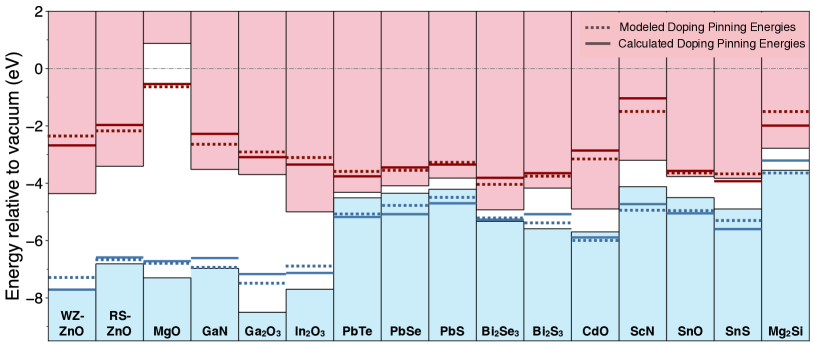
The dopability metrics and and the resulting doping pinning energies are shown in Fig. 6 alongside the absolute band edge positions for all 16 materials considered in this study. All energies are shown relative to the vacuum level. The and from defect calculations are represented as continuous lines while those resulting from the model, eq. (3), are depicted as dashed lines. The position of the pinning energies relative to the band edges determine the dopability of a material. For example, if the pinning energies and are both inside the corresponding bands (meaning and ), the compound allows both - and -type doping, likely to the degenerate levels. Conversely, if one of the doping pinning energies is inside the band gap, the dopability of the material to the corresponding carrier type is reduced and even diminished depending on the distance from the band edge. If both doping pinning energies are deep inside the band gap, the material cannot be doped.
As evident from the Fig. 6 as well as from the previous discussion there is a good overall correspondence between the calculated and modeled pinning energies. However, contrary to the Zunger’s finding for III-V and II-VI semiconductors, the doping pinning energies generally do not align. It is clear that if compounds outside these two groups are considered the deviations in the positions of the doping pinning levels are significant ( 2 eV). Hence, one can not rely on the alignment of the pinning levels and a simple doping principles based on the band edges alone.
Lot of emphasis has been given previously to the absolute position of the band edges as a guiding principle. In addition to the work of Zunger and co-workers 93, 107, Walukiewicz 108 and Schleife et al. 94 discussed how the band edge energies expressed relative to a universal branch-point energy correlate with dopability. In all of these works it was found that the -type dopable materials typically have high electron affinity (low ) while the -dopable ones have small ionization potentials (high ) 94, 109.
Absolute and also appear in our model as properties influencing materials dopability. Our derivation explains why they correlate with dopability, but also reveals that these are not the only relevant properties as one can clearly see that the dopability trends do not exactly correspond to the trends in the band edge positions. For example, GaN, Ga2O3 and In2O3 are all degenerately -dopable despite large differences in their positions. Also, SnO and SnS are only moderately -dopable while having their s below GaN, etc. An obvious question that follows from this discussion is whether a model of dopability that includes only the band edges can be constructed?
4.1 Description from the band edges alone
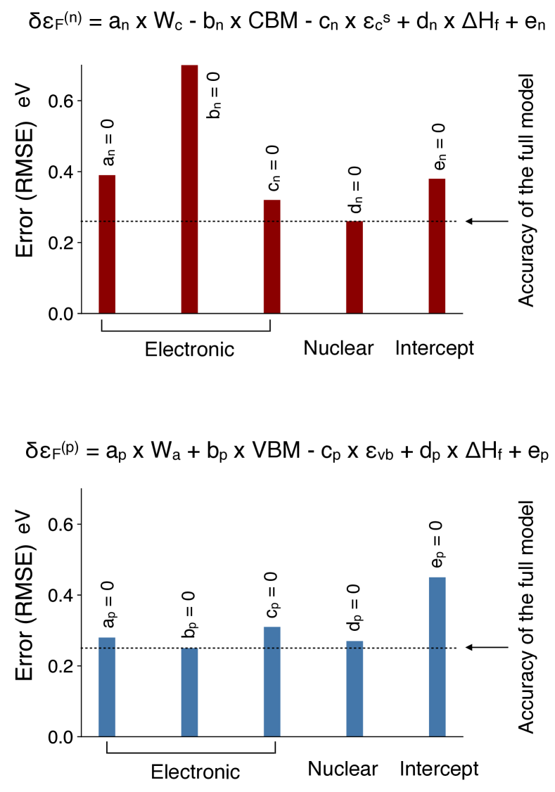
To answer this, we repeated the fitting exercise from validation section by only including the absolute band edge terms and the free parameter (intercept). The simplified dopability metrics are then given as and . The fit thus performed resulted in the root mean square errors (RMSE) of 0.67 eV and 0.41 eV for the - and -type dopability, respectively; compared to the RMSE of 0.26 eV (-type) and 0.25 eV (-type) for the full model. So, using only the band edge positions as descriptors of dopability is much less accurate than the full model.
Including the work functions to the two metrics, and , helps improve the model significantly to RMSE = 0.34 (-type) and 0.31 (-type). This further supports one of the key implications of our model. It is not the absolute and that matter, but the and relative to the average electronic energies of the elements, which are in this case represented by their work functions. That said, the absolute and could serve as coarse guidelines but one needs to be aware that the error in the doping pinning energies can likely be much above 0.5 eV.
Furthermore, to gauge the importance of each individual term, we performed an exercise of removing terms one at a time (by putting their coefficient to zero), and re-doing the fit. As discussed previously, these terms can be grouped into electronic contributions, comprising of reference phase work function (), absolute band edge positions ( or ), average electronic energy of cation- () or valence band states () and nuclear repulsion (), plus a free parameter (intercept term ). Based on the results (RMSE values) summarized in Fig. 7, we can draw following conclusions: (1) -type doping metric depends more significantly on the electronic contributions than the p-type doping metric , (2) within the electronic terms, both the reference phase work function and compounds’ CBM are needed to accurately reproduce both and , and finally, (3) the intercept is important, especially in case of . Please note, that the intercept integrates both electronic and nuclear contributions that are not easily separated.
4.2 Role of the band gap
Magnitude of the electronic band gap is another quantity used to gauge dopability of semiconductors. It follows from the observation that wider the gap is, more insulating or less dopable a material is likely to be. While generally true, this coarse rule of thumb does not provide any insight into the apparent doping asymmetry (typically towards -type) of many semiconductors. Also, there are exceptions from this rule like MgO for example. MgO is a large band gap (7.7 eV) material and is moderately -type dopable 110, which is in agreement with the predicted -doping pinning energy that appear near the in Fig. 6. Our approach shows that the band gap of the material does not appear to be a governing factor in determining dopability. What matters are the positions of individual band edges, characteristic electronic energy of the corresponding reference phase, average band energies, band widths, and nuclear repulsions due to creation of a defect.
The only place where the band gap explicitly appears is in the -type dopability when limited by the anion interstitials (see Dopability metric section. One of the conditions demands that the difference between the center of the valence band and the conduction band minimum be as large as possible. Since , the only way to accomplish this is to have to be as close to , which implies having narrow valence band width and small band gap, both at the same time. However, since the anion interstitials are rarely low energy defects in binary systems the explicit role of the band gap is not very prominent.
However, the likelihood for the conditions for the vacancy limited - and -type dopability to be simultaneously fulfilled is higher in low gap systems although not exclusively. Recall that the approximate way to treat average electronic energies of the reference phases is to assume they are close to the conduction and valence band centers. Then, the ambipolar dopability demands large bandwidths for both valence and conduction bands. This is more often the case in narrow gap systems than in wide gap systems, although one cannot neglect exceptions to this relatively naive expectation. There is nothing that in principle forbids moderate to wide gap systems to have large bandwidths and there are also tradeoffs with other properties that could make up for the bands that are not as wide.
4.3 Extrinsic defects, covalent and multinary systems and the utility in materials searches
Dopability of a semiconductor can also depend on the availability of an appropriate external dopant. The dopant’s effectiveness, in addition to the host material not developing intrinsic compensating defects (the subject of this paper), will depend on: (1) its solubility in the host material, and (2) its preference toward the expected behavior (donation or acceptance of charges). For example, as Fig. 6 suggests ZnO in its ground state wurtzite structure should be moderately -type dopable. Not to degenerate levels, but nevertheless it should be possible to dope it -type. Based on the solubility among the external dopants, Li (group-I) and N (group-V) are best suited for this purpose. However, Li fails to dope ZnO -type because it is present in nearly equal amount both as a substitutional acceptor (Li) and as interstitial donor (Li). Hence, it almost self-compensates resulting in a very low net hole concentrations. N on the other hand act as a deep acceptor in ZnO, and need high ionization energy to provide any measurable free carriers at room temperature. In ZnO, -type doping is also made difficult because of the presence of hydrogen (acting as a donor) as an unintentional contaminant during growth techniques 82, 26, 111.
In principle our model can be extended to include extrinsic defects. This would require knowledge of the position of the atomic orbitals of extrinsic dopants relative to the band edges of the host as well as assumptions (or a model) pertaining to the defects states within the host. Also, the present model is developed for ionic and partially ionic semiconductors. Therefore, it is not expected to apply to fully covalent systems such as the elemental Si, Ge, diamond, and other. In these cases, defects such as vacancies introduce states deep inside the band gap, in addition to renormalizing the valence and conduction band density of states. Such deep defect states can both accept and donate charges, and hence, can limit both the - and -type doping. While the model can be extended to cover fully covalent materials, in this paper we have focused on ionic or partially ionic semiconductors as they constitute a larger group of materials.
The model description would also become much more complex if one moves beyond the elemental and binary semiconductors. In ternary and multinary systems, generally more than one atomic specie contributes to the band edges, and therefore, it is likely that more than one model is required to cover different possible situations. Alternatively, for specific families among multinary compounds, such as Zintl phases for example, one could try finding some other higher-level descriptors that could be helpful in large scale materials searches 112.
Lastly, in regard to the large scale materials screening for dopability, the model we have developed could be useful, especially the version involving proxies from the validation section, provided that a rapid evaluation of the absolute (or relative) , and elemental work functions can be made possible. While the band edges are not the only governing properties their contributions to the dopability of semiconductors cannot be ignored, not even approximately. The computational procedure to evaluate absolute and is nowadays well established; it includes the electronic structure calculations for the bulk in combination with the calculations of the surface dipoles. The surface calculations represent a real bottleneck to high-throughput screening as they are of the similar level of complexity as the direct defect calculations. So, until a more efficient way to evaluate absolute and position is developed, relatively tedious and laborious direct defect calculations remain the only available choice for a robust predictions of the doping tendencies of materials.
5 Conclusions
In conclusion, in order to reveal the intrinsic materials properties that determine dopability of semiconductors, we have developed a model description of the defect formation energies in ionic and partially ionic systems. The model is constructed using the tight-binding description of the electronic structure augmented by the nuclear repulsion (pair) potential term. Utilizing such an approach in combination with the existing formulation of the dopability in terms of the limiting (compensating) intrinsic point defects, we are able to analytically separate various contributions. Contrary to the presently adopted and largely heuristic view, the position of the band edges alone cannot be used to accurately describe the doping limits of semiconductors. In addition, the electronic structure of the elemental reservoirs has to be taken into account as well as the differences in the nuclear repulsion between the material of interest and the elemental reservoirs. Hence, the dopability of semiconductors is a result of a relatively complex tradeoffs between various intrinsic properties. To make the model practical, as well as for the purpose of validation, we replace the hard-to-calculate quantities in the model with the more accessible ones and showed that model is able to accurately reproduce the directly calculated (from modern defect calculations) doping limits of 16 classic binary semiconductors. Lastly, we discuss the extension of our work to more complex chemistries and the utility in large-scale material searches.
6 Methods
First-principles defect calculations. In this work we employ the standard supercell approach 113 using our computational framework 114 to calculate formation energies of point defects using the following equation:
| (13) |
where represents the formation energy of a point defect D in charge state . and are the total energies of the supercells with and without the defect, respectively. is the chemical potential of atomic species, , describing exchange of particles with the respective reservoirs. is the Fermi energy and is used here to account for the possible exchange of charge between the defect and the Fermi energy (i.e. the charge reservoir). is a correction term to accounts for the finite-size corrections within the supercell approach 113. The chemical potential is expressed relative to the reference elemental chemical potential , calculated using the FERE approach 115 (re-fitted for HSE calculations,), and is the deviation from the reference elemental phase, the bounds of which are determined by the thermodynamic phase stability.
A plane wave energy cutoff of 340 eV, and a Monkhorst-Pack k-point sampling116 is used. The low-frequency total (electronic + ionic) dielectric constant is obtained following the procedure in Ref.117. We have implemented tools in our framework114 to calculate the following finite-size corrections: (1) potential alignment, (2) image-charge correction, and (3) band filling correction to address Moss-Burstein-type effects. Beyond the finite-size effects, another source of inaccuracy arises from the well-known DFT band gap problem. Accurate band gaps are needed to correctly describe the formation energy of charged defects as a function of the electronic chemical potential i.e., Fermi energy. We employ state-of-the-art GW quasiparticle energy calculations118 to compute band edge shifts (relative to the DFT-computed band edges). The band edge shifts are used to correct the defect formation energy in multiple charge states. GW calculations are performed on the DFT relaxed structures, with the unit cell vectors re-scaled to match the experimental lattice volume117. For hybrid functional (HSE06119, 120) calculations, the the exchange mixing is used accordingly to match their experimental lattice parameters and band gaps. Having defect formation energy allows thermodynamic modeling of defect and carrier concentrations, computed here using the approach from Refs. 36, 87, 121 Confidence in our predictions stems from the correct description of defects and doping in our previous works 36, 87, 114demonstrating good agreement between calculated and measured defect and charge carrier concentrations in PbTe and other systems.
We provide detailed tabulated data of defect formation energies and converged calculation parameters as *.csv files along with the supporting information containing additional details that may be necessary to validate our results and discussion presented in the main manuscript. This material is available at http://pubs.acs.org/.
The authors thank Dr. Stephan Lany from National Renewable Energy Laboratory (NREL) for fruitful discussions. We acknowledge support from NSF DMR program, grant no. 1729594 and 1729487. This research used computational resources sponsored by the DOE Office of Energy Efficiency and Renewable Energy and located at National Renewable Energy Laboratory. High-performance computational resources at Colorado School of Mines are also acknowledged.
References
- Williamson et al. 2017 Williamson, B. A. D.; Buckeridge, J.; Brown, J.; Ansbro, S.; Palgrave, R. G.; Scanlon, D. O. Engineering Valence Band Dispersion for High Mobility p-Type Semiconductors. Chemistry of Materials 2017, 29, 2402–2413
- Varley et al. 2017 Varley, J. B.; Miglio, A.; Ha, V.-A.; van Setten, M. J.; Rignanese, G.-M.; Hautier, G. High-Throughput Design of Non-oxide p-Type Transparent Conducting Materials: Data Mining, Search Strategy, and Identification of Boron Phosphide. Chemistry of Materials 2017, 29, 2568–2573
- Varley et al. 2014 Varley, J. B.; Lordi, V.; Miglio, A.; Hautier, G. Electronic structure and defect properties of from hybrid functional and many-body perturbation theory calculations: A possible ambipolar transparent conductor. Phys. Rev. B 2014, 90, 045205
- Burbano et al. 2011 Burbano, M.; Scanlon, D. O.; Watson, G. W. Sources of Conductivity and Doping Limits in CdO from Hybrid Density Functional Theory. Journal of the American Chemical Society 2011, 133, 15065–15072
- Sachet et al. 2015 Sachet, E.; Shelton, C. T.; Harris, J. S.; Gaddy, B. E.; Irving, D. L.; Curtarolo, S.; Donovan, B. F.; Hopkins, P. E.; Sharma, P. A.; Sharma, A. L.; Ihlefeld, J.; Franzen, S.; Maria, J.-P. Dysprosium-doped cadmium oxide as a gateway material for mid-infrared plasmonics. Nature Materials 2015, 14, 414–420
- Dou et al. 1998 Dou, Y.; Egdell, R.; Walker, T.; Law, D.; Beamson, G. N-type doping in CdO ceramics: a study by EELS and photoemission spectroscopy. Surface Science 1998, 398, 241–258
- Miller et al. 2018 Miller, S. A.; Dylla, M.; Anand, S.; Gordiz, K.; Snyder, G. J.; Toberer, E. S. Empirical modeling of dopability in diamond-like semiconductors. npj Computational Materials 2018, 4, 71
- Martinez et al. 2017 Martinez, A. D.; Fioretti, A. N.; Toberer, E. S.; Tamboli, A. C. Synthesis, structure, and optoelectronic properties of II–IV–V 2 materials. Journal of Materials Chemistry A 2017, 5, 11418–11435
- Biswas et al. 2012 Biswas, K.; Zhao, L.-D.; Kanatzidis, M. G. Tellurium-Free Thermoelectric: The Anisotropic n-Type Semiconductor Bi2S3. Advanced Energy Materials 2012, 2, 634–638
- Yu 2003 Yu, D. n-Type Conducting CdSe Nanocrystal Solids. Science 2003, 300, 1277–1280
- Kumar et al. 2013 Kumar, M.; Zhao, H.; Persson, C. Study of band-structure, optical properties and native defects in A I B III O 2 ( A I = Cu or Ag, B III = Al, Ga or In) delafossites. Semiconductor Science and Technology 2013, 28, 065003
- Ibuki et al. 2000 Ibuki, S.; Yanagi, H.; Ueda, K.; Kawazoe, H.; Hosono, H. Preparation of n -type conductive transparent thin films of AgInO2:Sn with delafossite-type structure by pulsed laser deposition. Journal of Applied Physics 2000, 88, 3067–3069
- Kumaravel and Ramamurthi 2011 Kumaravel, R.; Ramamurthi, K. Structural, optical and electrical properties of In-doped Cd2SnO4 thin films by spray pyrolysis method. Journal of Alloys and Compounds 2011, 509, 4390–4393
- Segev and Wei 2005 Segev, D.; Wei, S.-H. Structure-derived electronic and optical properties of transparent conducting oxides. Physical Review B 2005, 71, 125129
- Colston and Myronov 2018 Colston, G.; Myronov, M. Electrical properties of n-type 3C-SiC epilayers in situ doped with extremely high levels of phosphorus. Semiconductor Science and Technology 2018, 33, 114007
- Crandall 1968 Crandall, R. S. Electrical Conduction in n-Type Cadmium Sulfide at Low Temperatures. Physical Review 1968, 169, 577–584
- Walsh et al. 2008 Walsh, A.; Da Silva, J. L. F.; Wei, S.-H.; Körber, C.; Klein, A.; Piper, L. F. J.; DeMasi, A.; Smith, K. E.; Panaccione, G.; Torelli, P.; Payne, D. J.; Bourlange, A.; Egdell, R. G. Physical Review Letters 2008, 100, 167402
- Limpijumnong et al. 2009 Limpijumnong, S.; Reunchan, P.; Janotti, A.; Van De Walle, C. G. Hydrogen doping in indium oxide: An ab initio study. Physical Review B - Condensed Matter and Materials Physics 2009, 80, 1–4
- Stevanović et al. 2014 Stevanović, V.; Lany, S.; Ginley, D. S.; Tumas, W.; Zunger, A. Assessing capability of semiconductors to split water using ionization potentials and electron affinities only. Phys. Chem. Chem. Phys. 2014, 16, 3706–3714
- Kim et al. 2012 Kim, H. J.; Kim, U.; Kim, T. H.; Kim, J.; Kim, H. M.; Jeon, B.-G.; Lee, W.-J.; Mun, H. S.; Hong, K. T.; Yu, J.; Char, K.; Kim, K. H. Physical properties of transparent perovskite oxides (Ba,La)SnO3 with high electrical mobility. Physical Review B 2012, 86, 165205
- van Benthem et al. 2001 van Benthem, K.; Elsässer, C.; French, R. H. Bulk electronic structure of SrTiO3: Experiment and theory. Journal of Applied Physics 2001, 90, 6156–6164
- Tufte and Chapman 1967 Tufte, O. N.; Chapman, P. W. Electron Mobility in Semiconducting Strontium Titanate. Physical Review 1967, 155, 796–802
- Dimitrievska et al. 2016 Dimitrievska, M.; Ivetić, T. B.; Litvinchuk, A. P.; F̃airbrother, A.; Miljević, B. B.; Štrbac, G. R.; Pérez Rodríguez, A.; Lukić-Petrović, S. R. Eu 3+ -Doped Wide Band Gap Zn 2 SnO 4 Semiconductor Nanoparticles: Structure and Luminescence. The Journal of Physical Chemistry C 2016, 120, 18887–18894
- Ueda et al. 1992 Ueda, N.; Omata, T.; Hikuma, N.; Ueda, K.; Mizoguchi, H.; Hashimoto, T.; Kawazoe, H. New oxide phase with wide band gap and high electroconductivity, MgIn 2 O 4. Applied Physics Letters 1992, 61, 1954–1955
- Kawazoe and Ueda 2004 Kawazoe, H.; Ueda, K. Transparent Conducting Oxides Based on the Spinel Structure. Journal of the American Ceramic Society 2004, 82, 3330–3336
- Özgür et al. 2005 Özgür, Ü.; Alivov, Y. I.; Liu, C.; Teke, A.; Reshchikov, M. A.; Doǧan, S.; Avrutin, V.; Cho, S.-J.; Morkoç, H. A comprehensive review of ZnO materials and devices. Journal of Applied Physics 2005, 98, 1–103
- Nagasawa and Shionoya 1966 Nagasawa, M.; Shionoya, S. Exciton structure in optical absorption of SnO2 crystals. Physics Letters 1966, 22, 409–410
- Edwards et al. 2004 Edwards, P. P.; Porch, A.; Jones, M. O.; Morgan, D. V.; Perks, R. M. Basic materials physics of transparent conducting oxides. Dalton Transactions 2004, 2995
- Bellal et al. 2009 Bellal, B.; Hadjarab, B.; Bouguelia, A.; Trari, M. Visible light photocatalytic reduction of water using SrSnO3 sensitized by CuFeO2. Theoretical and Experimental Chemistry 2009, 45, 172–179
- Hadjarab et al. 2007 Hadjarab, B.; Bouguelia, A.; Trari, M. Synthesis, physical and photo electrochemical characterization of La-doped SrSnO3. Journal of Physics and Chemistry of Solids 2007, 68, 1491–1499
- Pearton et al. 2018 Pearton, S. J.; Yang, J.; Cary, P. H.; Ren, F.; Kim, J.; Tadjer, M. J.; Mastro, M. A. A review of Ga 2 O 3 materials, processing, and devices. Applied Physics Reviews 2018, 5, 011301
- Lany 2018 Lany, S. Defect phase diagram for doping of Ga2O3. APL Materials 2018, 6
- Yashima et al. 1998 Yashima, I.; Watanave, H.; Ogisu, T.; Tsukuda, R.; Sat̃o, S. Thermoelectric Properties and Hall Effect of Bi 2 Te 3 - x Se x Polycrystalline Materials Prepared by a Hot Press Method. Japanese Journal of Applied Physics 1998, 37, 2472–2473
- Filip et al. 2013 Filip, M. R.; Patrick, C. E.; Giustino, F. GW quasiparticle band structures of stibnite, antimonselite, bismuthinite, and guanajuatite. Physical Review B 2013, 87, 205125
- Hor et al. 2009 Hor, Y. S.; Richardella, A.; Roushan, P.; Xia, Y.; Checkelsky, J. G.; Yazdani, A.; Hasan, M. Z.; Ong, N. P.; Cava, R. J. p-type Bi2Se3 for topological insulator and low-temperature thermoelectric applications. Physical Review B 2009, 79, 195208
- Goyal et al. 2017 Goyal, A.; Gorai, P.; Toberer, E. S.; Stevanović, V. First-principles calculation of intrinsic defect chemistry and self-doping in PbTe. npj Computational Materials 2017, 3, 42
- Ohno et al. 2018 Ohno, S.; Imasato, K.; Anand, S.; Tamaki, H.; Kang, S. D.; Gorai, P.; Sato, H. K.; Toberer, E. S.; Kanno, T.; Snyder, G. J. Phase Boundary Mapping to Obtain n-type Mg3Sb2-Based Thermoelectrics. Joule 2018, 2, 141–154
- Shuai et al. 2015 Shuai, J.; Wang, Y.; Kim, H. S.; Liu, Z.; Sun, J.; Chen, S.; Sui, J.; Ren, Z. Thermoelectric properties of Na-doped Zintl compound: Mg3NaSb2. Acta Materialia 2015, 93, 187–193
- Zhang et al. 2017 Zhang, J.; Song, L.; Pedersen, S. H.; Yin, H.; Hung, L. T.; Iversen, B. B. Discovery of high-performance low-cost n-type Mg3Sb2-based thermoelectric materials with multi-valley conduction bands. Nature Communications 2017, 8, 13901
- Varley et al. 2013 Varley, J. B.; Schleife, A.; Janotti, A.; Van De Walle, C. G. Ambipolar doping in SnO. Applied Physics Letters 2013, 103
- Hosono et al. 2011 Hosono, H.; Ogo, Y.; Yanagi, H.; Kamiya, T. Bipolar Conduction in SnO Thin Films. Electrochemical and Solid-State Letters 2011, 14, H13
- Strauss 1961 Strauss, A. J. Electrical Properties of n-Type GaSb. Physical Review 1961, 121, 1087–1090
- Kolezynski et al. 2015 Kolezynski, A.; Nieroda, P.; Wojciechowski, K. T. Li doped Mg2Si p-type thermoelectric material: Theoretical and experimental study. Computational Materials Science 2015, 100, 84–88
- Nolas et al. 2007 Nolas, G. S.; Wang, D.; Beekman, M. Transport properties of polycrystalline Mg2Si1-ySby. Physical Review B 2007, 76, 235204
- Duong et al. 2016 Duong, A. T.; Nguyen, V. Q.; Duvjir, G.; Duong, V. T.; Kwon, S.; Song, J. Y.; Lee, J. K.; Lee, J. E.; Park, S.; Min, T.; Lee, J.; Kim, J.; Cho, S. Achieving ZT=2.2 with Bi-doped n-type SnSe single crystals. Nature Communications 2016, 7, 13713
- Kumagai et al. 2018 Kumagai, Y.; Tsunoda, N.; Oba, F. Point Defects and p-Type Doping in ScN from First Principles. Physical Review Applied 2018, 9, 34019
- Deng et al. 2015 Deng, R.; Ozsdolay, B. D.; Zheng, P. Y.; Khare, S. V.; Gall, D. Optical and transport measurement and first-principles determination of the ScN band gap. Physical Review B 2015, 91, 045104
- Saha et al. 2017 Saha, B.; Garbrecht, M.; Perez-Taborda, J. A.; Fawey, M. H.; Koh, Y. R.; Shakouri, A.; Martin-Gonzalez, M.; Hultman, L.; Sands, T. D. Compensation of native donor doping in ScN: Carrier concentration control and p -type ScN. Applied Physics Letters 2017, 110, 252104
- Fioretti et al. 2016 Fioretti, A. N.; Schwartz, C. P.; Vinson, J.; Nordlund, D.; Prendergast, D.; Tamboli, A. C.; Caskey, C. M.; Tuomisto, F.; Linez, F.; Christensen, S. T.; Toberer, E. S.; Lany, S.; Zakutayev, A. Understanding and control of bipolar self-doping in copper nitride. Journal of Applied Physics 2016, 119, 181508
- Vidal et al. 2012 Vidal, J.; Lany, S.; D’Avezac, M.; Zunger, A.; Zakutayev, A.; Francis, J.; Tate, J. Band-structure, optical properties, and defect physics of the photovoltaic semiconductor SnS. Applied Physics Letters 2012, 100
- Xiao et al. 2015 Xiao, Z.; Ran, F.-Y.; Hosono, H.; Kamiya, T. Route to n -type doping in SnS. Applied Physics Letters 2015, 106, 152103
- Bugajski and Lewandowski 1985 Bugajski, M.; Lewandowski, W. Concentration-dependent absorption and photoluminescence of n -type InP. Journal of Applied Physics 1985, 57, 521–530
- Neave et al. 1983 Neave, J. H.; Dobson, P. J.; Harris, J. J.; Dawson, P.; Joyce, B. A. Silicon doping of MBE-grown GaAs films. Applied Physics A Solids and Surfaces 1983, 32, 195–200
- Sun et al. 1991 Sun, S.; Armour, E.; Zheng, K.; Schaus, C. Zinc and tellurium doping in GaAs and AlGaAs grown by MOCVD. Journal of Crystal Growth 1991, 113, 103–112
- Su 2008 Su, C. H. Energy band gap, intrinsic carrier concentration, and Fermi level of CdTe bulk crystal between 304 and 1067 K. Journal of Applied Physics 2008, 103
- Segall et al. 1963 Segall, B.; Lorenz, M. R.; Halsted, R. E. Electrical Properties of n-Type CdTe. Physical Review 1963, 129, 2471–2481
- Nagaoka et al. 2018 Nagaoka, A.; Kuciauskas, D.; McCoy, J.; Scarpulla, M. A. High p-type doping, mobility, and photocarrier lifetime in arsenic-doped CdTe single crystals. Applied Physics Letters 2018, 112, 192101
- Simpson et al. 1992 Simpson, J.; Wallace, J. M.; Wang, S. Y.; Stewart, H.; Hunter, J. J.; Adams, S. J.; Prior, K. A.; Cavenett, B. C. N-type doping of molecular beam epitaxial zinc selenide using an electrochemical iodine cell. Semiconductor Science and Technology 1992, 7, 464–466
- Van De Walle et al. 1993 Van De Walle, C. G.; Laks, D. B.; Neumark, G. F.; Pantelides, S. T. First-principles calculations of solubilities and doping limits: Li, Na, and N in ZnSe. Physical Review B 1993, 47, 9425–9434
- Ueno et al. 2017 Ueno, K.; Fudetani, T.; Arakawa, Y.; Kobayashi, A.; Ohta, J.; Fujioka, H. Electron transport properties of degenerate n-type GaN prepared by pulsed sputtering. APL Materials 2017, 5, 126102
- Tsu et al. 1968 Tsu, R.; Howard, W. E.; Esaki, L. Optical and Electrical Properties and Band Structure of GeTe and SnTe. Physical Review 1968, 172, 779–788
- Tenga et al. 2009 Tenga, A.; Lidin, S.; Belieres, J.-P.; Newman, N.; Wu, Y.; Haeussermann, U. ChemInform Abstract: Metastable Cd 4 Sb 3 : A Complex Structured Intermetallic Compound with Semiconductor Properties. ChemInform 2009, 40, 15564–15572
- Hrubý et al. 1965 Hrubý, A.; Kubelík, I.; Štourač, L. Electrical conductivity and thermoelectric power of heavily doped P-type CdSb. Czechoslovak Journal of Physics 1965, 15, 740–746
- Böttger et al. 2011 Böttger, P. H. M.; Pomrehn, G. S.; Snyder, G. J.; Finstad, T. G. Doping of p-type ZnSb: Single parabolic band model and impurity band conduction. physica status solidi (a) 2011, 208, 2753–2759
- Liu et al. 2014 Liu, X.; Chen, J.; Luo, M.; Leng, M.; Xia, Z.; Zhou, Y.; Qin, S.; Xue, D.-J.; Lv, L.; Huang, H.; Niu, D.; Tang, J. Thermal Evaporation and Characterization of Sb 2 Se 3 Thin Film for Substrate Sb2Se3 /CdS Solar Cells. ACS Applied Materials & Interfaces 2014, 6, 10687–10695
- Chen et al. 2017 Chen, C.; Bobela, D. C.; Yang, Y.; Lu, S.; Zeng, K.; Ge, C.; Yang, B.; Gao, L.; Zhao, Y.; Beard, M. C.; Tang, J. Characterization of basic physical properties of Sb2Se3 and its relevance for photovoltaics. Frontiers of Optoelectronics 2017, 10, 18–30
- Shay et al. 1973 Shay, J. L.; Tell, B.; Buehler, E.; Wernick, J. H. Band Structure of ZnGeP2 and ZnSiP2 - Ternary Compounds with Pseudodirect Energy Gaps. Physical Review Letters 1973, 30, 983–986
- Heinemann et al. 2013 Heinemann, M.; Eifert, B.; Heiliger, C. Band structure and phase stability of the copper oxides Cu2O, CuO and Cu4O3. Physical Review B 2013, 87, 115111
- Bergum et al. 2018 Bergum, K.; Riise, H. N.; Gorantla, S.; Lindberg, P. F.; Jensen, I. J. T.; Gunnæs, A. E.; Galeckas, A.; Diplas, S.; Svensson, B. G.; Monakhov, E. Improving carrier transport in Cu 2 O thin films by rapid thermal annealing. Journal of Physics: Condensed Matter 2018, 30, 075702
- Ueda et al. 2004 Ueda, K.; Hosono, H.; Hamada, N. Energy band structure of LaCuOCh (Ch = S, Se and Te) calculated by the full-potential linearized augmented plane-wave method. Journal of Physics: Condensed Matter 2004, 16, 5179–5186
- Barati et al. 2009 Barati, A.; Klein, A.; Jaegermann, W. Deposition and characterization of highly p-type antimony doped ZnTe thin films. Thin Solid Films 2009, 517, 2149–2152
- Hiramatsu et al. 2003 Hiramatsu, H.; Ueda, K.; Ohta, H.; Hirano, M.; Kamiya, T.; Hosono, H. Degenerate p-type conductivity in wide-gap LaCuOSSe epitaxial films. Applied Physics Letters 2003, 82, 1048–1050
- Ahn and Park 2016 Ahn, D.; Park, S.-H. Cuprous halides semiconductors as a new means for highly efficient light-emitting diodes. Scientific Reports 2016, 6, 20718
- Yang et al. 2016 Yang, C.; Knei, M.; Lorenz, M.; Grundmann, M. Room-temperature synthesized copper iodide thin film as degenerate p-type transparent conductor with a boosted figure of merit. Proceedings of the National Academy of Sciences 2016, 113, 12929–12933
- Tate et al. 2009 Tate, J.; Ju, H. L.; Moon, J. C.; Zakutayev, A.; Richard, A. P.; Russell, J.; McIntyre, D. H. Origin of p-type conduction in single crystal CuAlO2. Physical Review B 2009, 80, 165206
- Kawazoe et al. 1997 Kawazoe, H.; Yasukawa, M.; Hyodo, H.; Kurita, M.; Yanagi, H.; Hosono, H. P-type electrical conduction in transparent thin films of CuAlO2. Nature 1997, 389, 939–942
- Ohta et al. 2002 Ohta, H.; Orita, M.; Hirano, M.; Yagi, I.; Ueda, K.; Hosono, H. Electronic structure and optical properties of SrCu2O2. Journal of Applied Physics 2002, 91, 3074–3078
- Kudo et al. 1998 Kudo, A.; Yanagi, H.; Hosono, H.; Kawazoe, H. SrCu2O2: A p -type conductive oxide with wide band gap. Applied Physics Letters 1998, 73, 220–222
- Akasaki 2015 Akasaki, I. Nobel Lecture: Fascinated journeys into blue light. Rev. Mod. Phys. 2015, 87, 1119–1131
- Amano 2015 Amano, H. Nobel Lecture: Growth of GaN on sapphire via low-temperature deposited buffer layer and realization of -type GaN by Mg doping followed by low-energy electron beam irradiation. Rev. Mod. Phys. 2015, 87, 1133–1138
- Nakamura 2015 Nakamura, S. Nobel Lecture: Background story of the invention of efficient blue InGaN light emitting diodes. Rev. Mod. Phys. 2015, 87, 1139–1151
- Janotti and Van de Walle 2009 Janotti, A.; Van de Walle, C. G. Fundamentals of zinc oxide as a semiconductor. Rep. Prog. Phys. 2009, 72, 126501
- Hosono et al. 2011 Hosono, H.; Paine, D. C.; Ginley, D. In Handbook of Transparent Conductors; Ginley, D. S., Ed.; Springer US: Boston, MA, 2011
- King and Veal 2011 King, P. D. C.; Veal, T. D. Conductivity in transparent oxide semiconductors. Journal of Physics: Condensed Matter 2011, 23, 334214
- Lany and Zunger 2009 Lany, S.; Zunger, A. Polaronic hole localization and multiple hole binding of acceptors in oxide wide-gap semiconductors. Phys. Rev. B 2009, 80, 085202
- Scanlon and Watson 2012 Scanlon, D. O.; Watson, G. W. On the possibility of p-type SnO2. J. Mater. Chem. 2012, 22, 25236–25245
- Goyal and Stevanović 2018 Goyal, A.; Stevanović, V. Metastable rocksalt ZnO is -type dopable. Phys. Rev. Materials 2018, 2, 084603
- Tamaki et al. 2016 Tamaki, H.; Sato, H. K.; Kanno, T. Isotropic Conduction Network and Defect Chemistry in Mg3Sb2-Based Layered Zintl Compounds with High Thermoelectric Performance. Advanced Materials 2016, 28, 10182–10187
- Ohno et al. 2018 Ohno, S.; Imasato, K.; Anand, S.; Tamaki, H.; Kang, S. D.; Gorai, P.; Sato, H. K.; Toberer, E. S.; Kanno, T.; Snyder, G. J. Phase Boundary Mapping to Obtain n-type Mg3Sb2-Based Thermoelectrics. Joule 2018, 2, 141 – 154
- Alberi et al. 2018 Alberi, K.; Nardelli, M. B.; Zakutayev, A.; Mitas, L.; Curtarolo, S.; Jain, A.; Fornari, M.; Marzari, N.; Takeuchi, I.; Green, M. L.; Kanatzidis, M.; Toney, M. F.; Butenko, S.; Meredig, B.; Lany, S.; Kattner, U.; Davydov, A.; Toberer, E. S.; Stevanovic, V.; Walsh, A.; Park, N.-G.; Aspuru-Guzik, A.; Tabor, D. P.; Nelson, J.; Murphy, J.; Setlur, A.; Gregoire, J.; Li, H.; Xiao, R.; Ludwig, A.; Martin, L. W.; Rappe, A. M.; Wei, S.-H.; Perkins, J. The 2019 materials by design roadmap. Journal of Physics D: Applied Physics 2018, 52, 013001
- Gorai et al. 2017 Gorai, P.; Stevanović, V.; Toberer, E. S. Computationally guided discovery of thermoelectric materials. Nature Reviews Materials 2017, 2, 17053 EP –
- Gorai et al. 2019 Gorai, P.; McKinney, R. W.; Haegel, N. M.; Zakutayev, A.; Stevanovic, V. A computational survey of semiconductors for power electronics. Energy Environ. Sci. 2019, –
- Zunger 2003 Zunger, A. Practical doping principles. Applied Physics Letters 2003, 83, 57–59
- Schleife et al. 2009 Schleife, A.; Fuchs, F.; Rödl, C.; Furthmüller, J.; Bechstedt, F. Branch-point energies and band discontinuities of III-nitrides and III-/II-oxides from quasiparticle band-structure calculations. Applied Physics Letters 2009, 94, 012104
- Woods-Robinson et al. 2018 Woods-Robinson, R.; Broberg, D.; Faghaninia, A.; Jain, A.; Dwaraknath, S. S.; Persson, K. A. Assessing High-Throughput Descriptors for Prediction of Transparent Conductors. Chemistry of Materials 2018, 30, 8375–8389
- Freysoldt et al. 2014 Freysoldt, C.; Grabowski, B.; Hickel, T.; Neugebauer, J.; Kresse, G.; Janotti, A.; Van de Walle, C. G. First-principles calculations for point defects in solids. Rev. Mod. Phys. 2014, 86, 253–305
- Lany and Zunger 2009 Lany, S.; Zunger, A. Accurate prediction of defect properties in density functional supercell calculations. Modelling and Simulation in Materials Science and Engineering 2009, 17, 084002
- Gorai et al. 2018 Gorai, P.; Ortiz, B. R.; Toberer, E. S.; Stevanović, V. Investigation of n-type doping strategies for Mg3Sb2. J. Mater. Chem. A 2018, 6, 13806–13815
- Chern et al. 2017 Chern, G.-W.; Barros, K.; Batista, C. D.; Kress, J. D.; Kotliar, G. Mott Transition in a Metallic Liquid: Gutzwiller Molecular Dynamics Simulations. Phys. Rev. Lett. 2017, 118, 226401
- Varley et al. 2017 Varley, J. B.; Samanta, A.; Lordi, V. Descriptor-Based Approach for the Prediction of Cation Vacancy Formation Energies and Transition Levels. The Journal of Physical Chemistry Letters 2017, 8, 5059–5063
- Verma and Bhardwaj 2006 Verma, A. S.; Bhardwaj, S. R. Correlation between ionic charge and ground-state properties in rocksalt and zinc blende structured solids. Journal of Physics: Condensed Matter 2006, 18, 8603–8612
- Wacke et al. 2011 Wacke, S.; Górecki, T.; Górecki, C.; Ksia̧żek, K. Relations between the cohesive energy, atomic volume, bulk modulus and sound velocity in metals. Journal of Physics: Conference Series 2011, 289, 012020
- Deml et al. 2015 Deml, A. M.; Holder, A. M.; O’Hayre, R. P.; Musgrave, C. B.; Stevanović, V. Intrinsic Material Properties Dictating Oxygen Vacancy Formation Energetics in Metal Oxides. The Journal of Physical Chemistry Letters 2015, 6, 1948–1953
- Lide R. 2009 Lide R., D., Ed. CRC Handbook of Chemistry and Physics, 90th ed.; CRC Press: Boca Raton, FL, 2009
- Kramida et al. 2018 Kramida, A.; Yu. Ralchenko,; Reader, J.; and NIST ASD Team, NIST Atomic Spectra Database (ver. 5.6.1), [Online]. Available: https://physics.nist.gov/asd [2016, January 31]. National Institute of Standards and Technology, Gaithersburg, MD., 2018
- Lany 2015 Lany, S. Semiconducting transition metal oxides. Journal of Physics: Condensed Matter 2015, 27, 283203
- Zhang et al. 2000 Zhang, S. B.; Wei, S.-H.; Zunger, A. Microscopic Origin of the Phenomenlogical Equilibrium “Doping Limit Rule” in n-Type III-V Semiconductors. Physical Review Letters 2000, 84, 1232–1235
- Walukiewicz 1988 Walukiewicz, W. Mechanism of Fermi-level stabilization in semiconductors. Physical Review B 1988, 37, 4760–4763
- Robertson and Clark 2011 Robertson, J.; Clark, S. J. Limits to doping in oxides. Physical Review B - Condensed Matter and Materials Physics 2011, 83, 1–7
- Tardío et al. 2002 Tardío, M. M.; Ramírez, R.; González, R.; Chen, Y. p -type semiconducting properties in lithium-doped MgO single crystals. Physical Review B 2002, 66, 134202
- McCluskey et al. 2015 McCluskey, M. D.; Corolewski, C. D.; Lv, J.; Tarun, M. C.; Teklemic hael, S. T.; Walter, E. D.; Norton, M. G.; Harrison, K. W.; Ha, S. Acceptors in ZnO. Journal of Applied Physics 2015, 117, 112802
- Gorai et al. 2019 Gorai, P.; Goyal, A.; Toberer, E. S.; Stevanović, V. A simple chemical guide for finding novel n-type dopable Zintl pnictide thermoelectric materials. J. Mater. Chem. A 2019, 7, 19385–19395
- Lany and Zunger 2009 Lany, S.; Zunger, A. Accurate prediction of defect properties in density functional supercell calculations. Modelling and Simulation in Materials Science and Engineering 2009, 17, 084002
- Goyal et al. 2017 Goyal, A.; Gorai, P.; Peng, H.; Lany, S.; Stevanović, V. A computational framework for automation of point defect calculations. Computational Materials Science 2017, 130, 1–9
- Stevanović et al. 2012 Stevanović, V.; Lany, S.; Zhang, X.; Zunger, A. Correcting density functional theory for accurate predictions of compound enthalpies of formation: Fitted elemental-phase reference energies. Physical Review B 2012, 85, 115104
- Monkhorst and Pack 1976 Monkhorst, H. J.; Pack, J. D. Special points for Brillouin-zone integrations. Physical Review B 1976, 13, 5188–5192
- Peng et al. 2013 Peng, H.; Scanlon, D. O.; Stevanovic, V.; Vidal, J.; Watson, G. W.; Lany, S. Convergence of density and hybrid functional defect calculations for compound semiconductors. Physical Review B 2013, 88, 115201
- Hedin 1965 Hedin, L. New Method for Calculating the One-Particle Green’s Function with Application to the Electron-Gas Problem. Physical Review 1965, 139, A796–A823
- Heyd et al. 2003 Heyd, J.; Scuseria, G. E.; Ernzerhof, M. Hybrid functionals based on a screened Coulomb potential. The Journal of Chemical Physics 2003, 118, 8207–8215
- Heyd et al. 2006 Heyd, J.; Scuseria, G. E.; Ernzerhof, M. Erratum: “Hybrid functionals based on a screened Coulomb potential” [J. Chem. Phys. 118, 8207 (2003)]. The Journal of Chemical Physics 2006, 124, 219906
- Biswas and Lany 2009 Biswas, K.; Lany, S. Energetics of quaternary III-V alloys described by incorporation and clustering of impurities. Physical Review B 2009, 80, 115206