Effects of filling, strain, and electric field on the Néel vector in antiferromagnetic CrSb
Abstract
CrSb is a layered antiferromagnet (AFM) with perpendicular magnetic anisotropy, a high Néel temperature, and large spin-orbit coupling (SOC), which makes it interesting for AFM spintronic applications. To elucidate the various mechanisms of Néel vector control, the effects of strain, band filling, and electric field on the magnetic anisotropy energy (MAE) of bulk and thin-film CrSb are determined and analysed using density functional theory. The MAE of the bulk crystal is large (1.2 meV per unit cell). Due to the significant ionic nature of the Cr-Sb bond, finite slabs are strongly affected by end termination. Truncation of the bulk crystal to a thin film with one surface terminated with Cr and the other surface terminated with Sb breaks inversion symmetry, creates a large charge dipole and average electric field across the film, and breaks spin degeneracy, such that the thin film becomes a ferrimagnet. The MAE is reduced such that its sign can be switched with realistic strain, and the large SOC gives rise to an intrinsic voltage controlled magnetic anisotropy (VCMA). A slab terminated on both faces with Cr remains a compensated AFM, but with the compensation occurring nonlocally between mirror symmetric Cr pairs. In-plane alignment of the moments is preferred, the magnitude of the MAE remains large, similar to that of the bulk, and it is relatively insensitive to filling.
I Introduction
Antiferromagnetic (AFM) materials are of great interest for future spintronics applicationsBaltz et al. (2018). Their resonant frequencies are much higher than those of ferromagnetic (FM) materials, which allows them to be used in the THz applications Jungwirth et al. (2016); Gomonay and Loktev (2014); Keffer and Kittel (1952) and ultrafast switching Lopez-Dominguez et al. (2019). However, it is challenging to control and detect the antiferromagnetic states. There are several methods to control the spins in AFMs such as via exchange bias with a proximity FM layerNogués and Schuller (1999) and the use of electric current by Néel spin-orbit torque Wadley et al. (2016). The latter method has been extensively studied, although the results have recently been questioned Chiang et al. (2019); Churikova et al. (2020). Controlling the Néel vector without electric current is promising for ultra low power applications, since it has been predicted that magnetization reversal can be achieved with atto joule (aJ) level energy consumption Semenov et al. (2017). Electric field control of the magnetic properties of AFMs can be realized indirectly through the mechanism of mechanical strain created from a piezoelectric substrate Barra et al. (2018); Yan et al. (2019); Park et al. (2019); Chen et al. (2019); Wang et al. (2019a); Boldrin et al. (2018); Liu et al. (2018) or a combination of strain plus exchange spring Feng et al. (2020). It can also be realized directly through the mechanism of voltage controlled magnetic anisotropy (VCMA). This mechanism has been experimentally and theoretically studied for FMs Duan et al. (2008); Nakamura et al. (2009); Niranjan et al. (2010); Amiri and Wang (2012); Alzate et al. (2014); Nozaki et al. (2014); Ong et al. (2015); Skowroński et al. (2015a, b); Hibino et al. (2015); Nozaki et al. (2016); Shiota et al. (2017); Zhang et al. (2017); Wen et al. (2017); Kozioł-Rachwał et al. (2017); Kawabe et al. (2017); Li et al. (2017); Kato et al. (2018); Kwon et al. (2019a, b); Nozaki et al. (2020); Chen et al. (2020), and the experimental results have been recently reviewed.Miwa et al. (2018) Technological applications have been described and analysed Wang et al. (2015); Kang et al. (2017, 2016). More recently, several theoretical studies of VCMA in the AFM materials FeRh, MnPd, and MnPt have been reported Zheng et al. (2017); Lopez-Dominguez et al. (2019); Su et al. (2020); Chang et al. (2020).
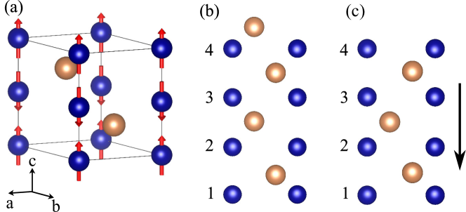
CrSb crystallizes in the hexagonal NiAs-type structure, and the spins on the Cr atoms couple ferromagnetically within the hexagonal plane and antiferromagnetically along the hexagonal axis as shown in Fig. 1(a). In the ground state, the Néel vector aligns along the hexagonal axis ([0001] direction), so that it has perpendicular magnetic anisotropy (PMA). The bands near the Fermi energy are composed of the d-orbitals of the Cr atoms, and these bands give rise to a large peak in the density of states near the Fermi energy.Dijkstra et al. (1989); Ito et al. (2007); Kahal et al. (2007); Polesya et al. (2011) The Sb atoms provide significant SOC. CrSb has a high Néel temperature (705 K) making it suitable for on-chip applications Takei et al. (1963). Recently, CrSb has been used to control the magnetic textures and tune the surface states of topological insulators He et al. (2017, 2018); Wang et al. (2019b).
We examine three different physical mechanisms that alter the magnetic anisotropy of bulk and thin-film CrSb: (i) strain, (ii) electron filling, and (iii) electric field. Density functional theory (DFT) calculations of the magnetostriction coefficient, strain coefficient, filling coefficient, and VCMA coefficient characterize the effectiveness of the three methods in modifying the MAE.
II Methods
We perform first principles calculations as implemented in the Vienna Ab initio Simulation Package (VASP) Kresse and Hafner (1993) to investigate the effects of strain, electric field, and band filling on the magnetic anisotropy of CrSb. Projector augmented-wave (PAW) potentials Blöchl (1994) and the generalized gradient approximation (GGA) parameterized by Perdew-Burke-Ernzerhof (PBE) are employed Perdew et al. (1996). A cut-off energy of 500 eV and 8 8 8 -centered k-point grid were used to make sure the total energy converged within eV per unit cell. A GGA+ implementation was also used to reproduce the magnetic moment on the Cr atom corresponding to the experimental values Snow (1952). We used eV for the Cr atom where .
From the initial bulk structure, uniaxial strain along the -axis is applied and the structure is fully relaxed along and axes until all forces on each atom are less than eVÅ-1. Here, the and axes are parallel to the and lattice vectors of the hexagonal unit cell shown in the Fig. 1. The strain is defined as where and are the lattice constants along with and without strain, respectivley. The calculated lattice constants without strain are Å and Å, which are close to those from experiment Snow (1952).
To obtain the charge density, a spin-polarized self-consistent calculation is performed with the relaxed structure for each strain. Using the obtained charge densities, and , are calculated in the presence of SOC where and are the total energies per unit cell with the Néel vector along [1000] and [0001] directions, respectively. The magnetic anisotropy energy (MAE) is defined as . For uniformity of comparison between bulk and thin-film structures, all values of are reported per bulk unit cell (u.c.) (i.e. per two Cr atoms). For MAE calculations, a denser k-point grid (16 16 16) is used for accuracy. The same procedures are performed to investigate the effect of electron filling on the MAE, and the structures are optimized for each number of electrons in the unit cell.
Charge transfer between the Cr and Sb ions is analyzed by calculating both the Bader charges Henkelman et al. (2006) and the planar averaged volumetric charge densities Wang et al. (2020). The “net electronic charge” on each atom is defined as the number of valence electrons for a given atom minus the Bader charge on the atom in units of . Thus, a depletion of electrons is a positive electronic charge. The Bader charges are used to understand the effect of truncation of the bulk to a slab and the application of an electric field. For thin-films, the planar averaged volumetric charge densities at different electric fields are calculated by averaging the three-dimensional charge density over the plane for fixed positions on the axis.
To investigate the effect of strain and electric field on the MAE of thin-film CrSb, we consider slab structures consisting of 2 and 3 unit cells along the -axis ( 1.1 nm and 1.6 nm). A 15 Å vacuum layer is included. The stability of two different surface terminations is quantified by calculating the cohesive energy defined as where is the total number of atoms, is the total energy of the relaxed slab structure, and is the sum of the energies of the individual atoms. For the thin-film structures, a 23 23 1 -centered k-point grid with a 500 eV cutoff energy is used to ensure the same convergence criteria as the bulk structure. The structures are fully relaxed until all forces on each atom are less than eVÅ-1 without changing the volume. Vertical external electric fields are applied to the slab by introducing a dipole layer in the middle of the vacuum layer. The dipole layer also corrects for the built in dipole moment in the CrSb slab structures to prevent interactions between the artificial periodic images Neugebauer and Scheffler (1992); Makov and Payne (1995). The equilibrium charge density is obtained by performing a spin-polarized self-consistent calculation without the electric field. Then, the charge densities with increasing applied electric fields along c-axis are obtained by relaxing the charges from the calculation with the previous electric field. For each electric field, the MAE is calculated using a k-point grid.
III Results and Discussion
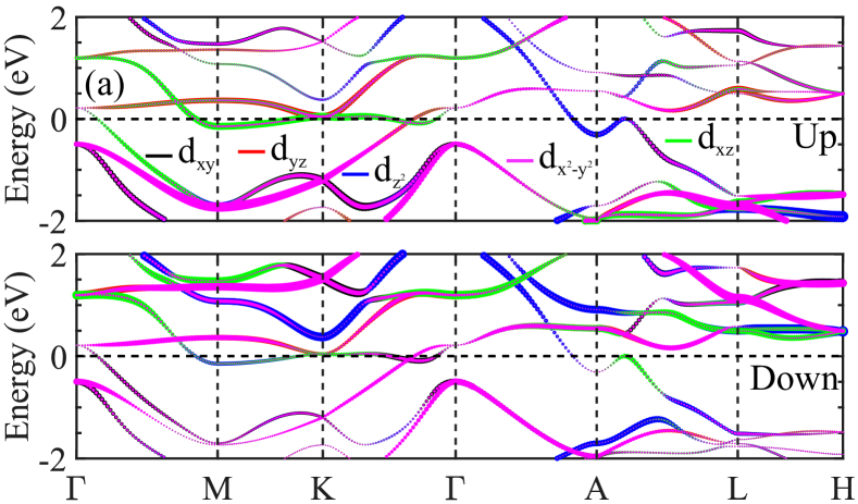
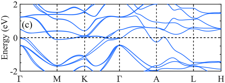
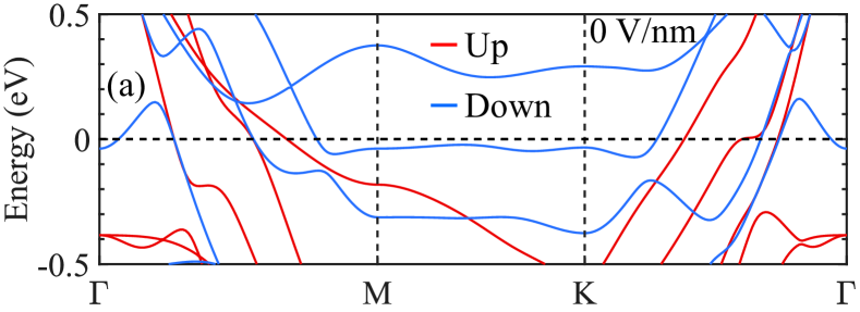
In Fig. 2, the electronic bandstructure of bulk CrSb is shown. Fig. 2(a) is the d-orbital resolved bandstructure for a Cr atom in equilibrium in the absence of SOC. The colors denote different orbitals as indicated by the legends, and the line thicknesses denote the relative occupations. The spin-up bands are shown in the top panel, and the spin-down bands are shown in the bottom panel. Fig. 2(c) shows the equilibrium bandstructure in the presence of SOC.

The effect of spin-orbit coupling (SOC) on the bandstructure is relatively large. A comparison of Fig. 2(a) to 2(c) shows that the SOC breaks the spin degeneracy throughout much of the Brillouin zone and creates anti-crossings at a number of band-crossing points. The largest band splitting occurs at . The two bands that touch at 0.2 eV in the absence of SOC are split by eV and the hole like band is pushed down below .
Fig. 3(a) shows plotted as a function of applied strain for bulk CrSb. The value at zero strain is meV/u.c. The positive sign of the MAE means that the Néel vector aligns along the c-axis (out-of-plane) independent of the strain. The monotonic increase in the MAE indicates that CrSb behaves like a magnet with a negative magnetostriction coefficient, since the tensile strain favors out-of-plane anisotropy. The magnetostriction coefficient () is defined as
| (1) |
where , , and are the Possion’s ratio (0.288), Young’s modulus (78.3 GPa), and strain, respectively Yu et al. (2015). The magnetoelastic anisotropy constant, , is calculated from the difference between two MAEs with and without strain (i.e., ). The parameters and are taken from a previous study Charifi et al. (2018). The calculated for small strain (between to ) is 19.8 ppm. CrSb has a negative value of , and the magnitude of is similar to that of MnNi and MnPd Park et al. (2019). We also define a strain coefficient as evaluated at . The value for bulk CrSb is meV/%strain.
The response of the bulk MAE as a function of the electron number in the unit cell is shown in Fig. 4. In equilibrium, the unit cell has 22 valence electrons, which is denoted by the vertical line in the figure. The MAE decreases most rapidly when the CrSb is depleted, and it changes sign when the hole doping reaches 0.75/u.c. For electron depletion, the filling coefficient, defined as , is 2.92 meV, where is the electron number per unit cell.

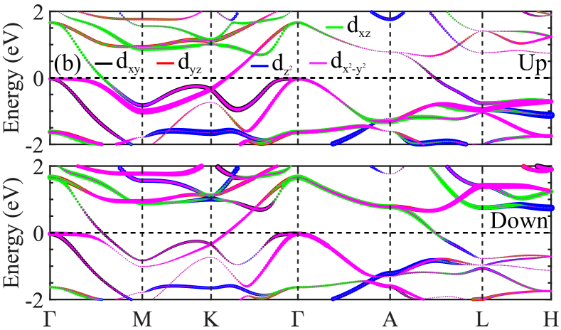
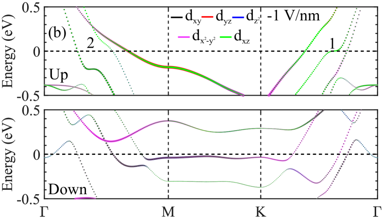
To understand the physical origin of the transition due to charge depletion, we consider the d-orbital resolved band structures for a Cr atom plotted for 2 different electron numbers in the unit cell, 22 (equilibrium) in Fig. 2(a) and 21 in Fig. 2(b). Within second-order perturbation theory, the MAE is approximately expressed asWang et al. (1993)
| (2) | ||||
where (), (), and are the (un)occupied states, (un)occupied eigenvalues, and the spin-orbit coupling constant, respectively. and are the out-of plane and in-plane components of the orbital angular momentum operator, and and denote spin-up and spin-down. The non-zero matrix elements in the Eq. (2) are , , , , , , , and . The largest contributions to Eq. (2) come from pairs of nearly degenerate occupied and unoccupied states near the Fermi level. In equilibrium (Fig. 2(a)), the main contributions to the MAE come from the spin-orbit coupling between occupied and unoccupied states at the point and near the point, and between occupied and unoccupied states near the point. All of these states couple through the operator, which results in the positive MAE value (out-of-plane anisotropy). When CrSb is depleted (see Fig. 2(b)), the entire band structure moves upward so that the main contributor states of the perpendicular anisotropy become unoccupied. This reduces the value of the MAE, and eventually reverses the sign for .
Below, we will compare the sensitivity of the bulk crystal MAE to electron filling with the sensitivity of the thin-film MAE to applied electric field. Such a comparison requires a common metric based on a common physical quantity that governs the MAE. Assuming that the common driving mechanism is the population change of the magnetic Cr atoms Zhang et al. (2017), we determine a slightly different parameter,
| (3) |
where is the average electron number on the Cr atoms as determined from the Bader charges. Due to the strongly ionic nature of the Cr-Sb bond, only of the hole doping goes to the Cr sublattice. The equilibrium charge resulting from a transfer of electrons from the Cr atom to the Sb atom is shown in Fig. 5(a), and the change in charge at a filling of -0.5 electrons / u.c. is shown in Fig. 5(b). The filling of -0.5 electrons / u.c. corresponds to -0.07 electrons / Cr atom. Using the values from Fig. 5(b), for hole doping, meV.
We now consider thin-film slabs with thicknesses of 2 and 3 unit cells corresponding to 1.1 nm and 1.6 nm, respectively. For the thinner slab, the cohesive energies are calculated for a 7 atomic layer structure of alternating Cr and Sb layers terminated on both ends with a Cr layer and for a 8 atomic layer structure (2 unit cells) terminated on one end with Cr and on the other with Sb. The cohesive energies of the 7 and 8 atomic layer structures are -3.328 eV and -3.517 eV, respectively. For the thicker slab, cohesive energies are calculated for an 11 atomic layer structure and a 12 atomic layer structure, and the cohesive energies are -3.522 eV and -3.636 eV, respectively. Thus, the slab strucures with an integer number of unit cells such that one face is a Cr layer and the opposing face is an Sb layer are the most stable, and they are the ones that we will consider first. We will refer to these structures as asymmetric slabs.
In these asymmetric slabs, inversion symmetry is broken, since one end is terminated with a Cr layer and the other end is terminated with a Sb layer. Thus, these thin films are also Janus structures. The two unit cell asymmetric thin-film is shown in Fig. 1(b). Below, results for strain and VCMA coefficients are presented for both the 2 and 3 unit cell asymmetric thin-films, and the in-depth microscopic analysis of the charge, magnetic moments, and electronic structure focuses on the 2 unit cell asymmetric thin-film.
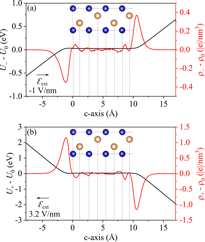
In the asymmetric thin films, there is a net polarization of electron charge between the positively charged Cr layer on the bottom and the negatively charged Sb layer on the top. The excess charges on each atom, as determined from the Bader charges, in the bulk and in the 2 unit-cell slab are shown in Fig. 5(a,c), and it is clear that, in the slab, the charge transfer is no longer balanced layer-by-layer. The net charge polarization gives rise to a built-in electric field that alternates positively and negatively within the slab, but, its average value points from the positive Cr layer on the bottom to the negative Sb layer on the top. This built-in electric field results in a built-in potential across the slab of 1.7 eV as shown by the plot of the equilibrium planar averaged Hartree potential in Fig. 5(d).
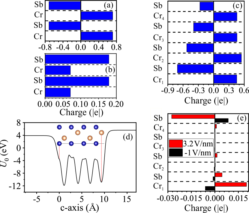
The truncation of the bulk to a finite slab results not only in a loss of local balance between the positive and negative charges, but also in a global imbalance of the magnetic moments of the Cr ions. In other words, the cancellation of magnetic moments between alternating layers of Cr is no longer exact, and a small net magnetic moment exists in the slab. The magnetic moments on each Cr atom are listed in the ‘’ column of Table 1 with the numbering of the Cr atoms corresponding to that shown in Fig. 1(b). The magnitudes of the magnetic moments in the Cr layers monotonically decrease from bottom to top as the Cr atoms approach the Sb terminated end of the slab. The breaking of the spin degeneracy is readily apparent in the bandstructure of the slab shown in Fig. 6(a). The degeneracy between the up-spin and down-spin bands is broken, and the CrSb slab has become a ferrimagnet (FiM). The breaking of the spin degeneracy of the AFM states in a finite slab of a layered AFM is explained by a simple chain model with different end terminations described in [NDj, ]. The wavefunctions of a pair of degenerate AFM states are weighted differently on alternate atoms of the magnetic lattice. Thus, the coupling of the two states to an end atom is different, and this different coupling breaks the degeneracy of the two states.
| Atom | |||
|---|---|---|---|
| Cr1 | 3.035 | 3.763 | 3.905 |
| Cr2 | 3.035 | 3.190 | 2.994 |
| Cr3 | 3.116. | 2.994 | |
| Cr4 | 2.889. | 3.904 |
A third result of truncating the bulk to a slab is that the MAE decreases. For the 1.1 nm slab, the MAE is reduced by a factor of 15 from 1.2 meV/u.c. to 0.079 meV/u.c. (0.17 erg/cm2), and for the 1.6 nm slab, the MAE is reduced by a factor of 2.1 to 0.58 meV/u.c. (1.85 erg/cm2). Also, the sensitivity of the MAE to strain increases. The strain coefficients of the 1.1 and 1.6 nm slabs () increase from 0.013 meV/%strain in the bulk to 0.068 meV/%strain and 0.062 meV/%strain, respectively, where the energies are per bulk unit cell (2 Cr atoms). The combined result of the reduced MAE and increased strain coefficient is that a 1.5% uniaxial compressive strain along [1000] direction in the 1.1 nm thin film causes a rotation of the Néel vector from out-of-plane to in-plane as shown in Fig. 3(b).
A fourth result is that the MAE also becomes sensitive to an external electric field as shown in Fig. 7. In other words, the thin slab exhibits intrinsic VCMA. Typically VCMA is found when a magnetic layer is placed in contact with a heavy-metal layer that provides SOC. However, the Sb layers provide large SOC, and the terminating Sb layer serves as the HM layer, such that the CrSb slab has intrinsic VCMA. The MAE decreases linearly as the electric field is increased, and, for the 1.1 nm slab, it changes sign at 3.2 V/nm, which indicates that the Néel vector rotates 90∘ from out-of-plane to in-plane.

The standard metric describing the sensitivity of the MAE to the applied electric field is given by the VCMA coefficient defined as
| (4) |
where is the MAE per unit area of the slab, is the external electric field and and are the electric field and the relative dielectric constant in the insulator, repectively. In a typical experiment, the insulator would be an oxide layer with . In our case, the insulator is the vacuum, so that and . The values of , evaluated at V/nm, are 76.4 fJV-1m-1 for the 1.1 nm film and 55.3 fJV-1m-1 for the 1.6 nm slab.
The calculated magnitudes of are comparable with many of the experimentally measured values of from heavy metal/FM/MgO heterostructures, Shiota et al. (2017); Kawabe et al. (2017); Skowroński et al. (2015a, b); Li et al. (2017); Nozaki et al. (2014); Hibino et al. (2015); Wen et al. (2017) with magnitudes ranging from 65 fJV-1m-1 in a Ta/Co0.25Fe0.55B0.20/MgO structure Shiota et al. (2017) to 139 fJV-1m-1 in a Ru/Co2FeAl/MgO structure. Wen et al. (2017) However, they are considerably smaller than the values of 370 fJV-1m-1 and 1043 fJV-1m-1 measured in Cr/Fe/MgO and Ir/CoFeB/MgO structures, respectively. Kozioł-Rachwał et al. (2017); Kato et al. (2018) A lengthy table of experimental values compiled from the literature is provided in a recent review Miwa et al. (2018). Theoretical studies of AFM materials have calculated magnitudes of both larger and smaller than the values for CrSb. For a G-AFM FeRh/MgO bilayer, the magnitude of was in the range of 130 to 360 fJV-1m-1 depending on the sign of the electric field, the strain, and the termination layer of either Fe or Rh Zheng et al. (2017). A value of 22.6 fJV-1m-1 was calculated for Pt/MnPd with vacuum as the dielectric Su et al. (2020). VCMA calculations of a MgO/MnPt/MgO slab found magnitudes of 170 fJV-1m-1 and 70 fJV-1m-1 depending on whether the MnPt layer was terminated on both ends with either Mn or Pt, respectively Chang et al. (2020).
To understand which Cr atoms contribute to the VCMA effect, we inspect the change in charge of the Cr atoms in response to the applied field. The change in charge with applied electric field, plotted in Figs. 5(e) and 8, shows that, among the Cr atoms, the only significant change in charge occurs on Cr1. This is to be expected, since the electric field is screened by the first and last atomic layers from the interior of the CrSb metal. The first atomic layer is Cr and the last is Sb, so that an applied field creates a net change in charge on the Cr sublattice with the charge being transferred to the Sb sublattice.
The sensitivities of the MAE of the thin film slabs to the average charging of the Cr atoms due to an applied electric field is comparable to the sensitivity of the bulk MAE to the filling of the Cr atoms. The values of evaluated at are 19.7 meV and 13.9 meV for the 2 layer and 3 layer slabs, respectively. For comparison, the bulk value for hole doping is meV. Thus, the sensitivity of the MAE per unit cell to the change in the average charge on the Cr atoms lies in the range of 13 - 20 meV for both of the slabs and the bulk.
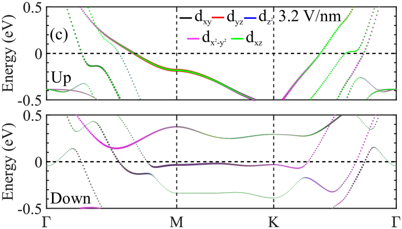
To elucidate the physical origin of switching mechanism in the two layer slab, the d-orbital resolved band structures for the Cr1 atom under different electric fields are plotted in Fig. 6(b,c). At the electric field of 1 V/nm, the major contribution of the perpendicular anisotropy comes from the spin-orbit coupling between the unoccupied and occupied states through operator in the region 1. Although the states in the region 1 are coupled through the in-plane angular momentum operator, the contribution of the MAE is positive since they are from different spin channels. In the region 2, the occupied states are coupled with unoccupied states through , which contributes the in-plane anisotropy. As the external field increases (see Fig. 6 (c)), the unoccupied states in the region 1 move away from the Fermi level by 18 meV, which results in the reduction of the out-of-plane anisotropy, since the denominator in the Eq. 2 increases. In addition, in the region 2, the occupied states move closer to the Fermi energy by 67 meV as the electric field increases so that the in-plane anisotropy increases.
Previous studies have shown that the choice of surface termination of a FM layer can alter, or even change the sign of the MAE Yang et al. (2011); Okabayashi et al. (2014); Zheng et al. (2017); Chang et al. (2020). Thin film CrSb is no exception. The final structure that we consider is the slab shown in Fig. 1(c). It is identical to the 1.1 nm thin film analyzed above, except that the top Sb layer is removed so that the thin film becomes mirror symmetric with respect to the plane. As a result, there is no net electrical dipole moment or built-in potential across the slab. The net magnetic moment of the slab remains zero, as shown in the last column of Table 1. The magnetic moment is no longer compensated locally in each unit cell; the compensation occurs between the mirror symmetric pairs of Cr atoms. Furthermore, the magnitude of the MAE ( meV / u.c) is more than an order of magnitude larger compared to that of the asymmetric slab ( meV / u.c), and it changes sign, so that in-plane alignment of the magnetic moments is preferred. The magnitude of the MAE is similar to that of the bulk ( meV / u.c), but with opposite sign. Note that the value of meV / u.c. is obtained by taking the total MAE of the slab and dividing by two, since it contains two unit cells of magnetic ions even though the last Sb layer of the top unit cell is missing.
Applying an electric field to this symmetric slab depletes electrons from the bottom Cr layer and accumulates electrons on the top Cr layer, so that the net change in charge on the Cr layers is zero. This is in contrast to the effect of an electric field on the antisymmetric slab where the applied field depletes electrons from the bottom Cr layer and accumulates electrons on the top Sb layer, with the overall effect being a net depletion of electrons on the Cr atoms. In the symmetric slab, with no net change in charge on the Cr atoms, the MAE remains unchanged to 4 significant digits over the range of V/nm. This is consistent with results of prior simulations of symmetric MgO / FM / MgO and MgO / AFM / MgO structures Duan et al. (2008); Chang et al. (2020).
To estimate the sensitivity of the MAE of the symmetric slab to electron filling, we alter the electron number of the slab by applying a compensating background charge, as we did in the bulk. Since the background charge is uniformly distributed throughout the simulation domain, which includes the vacuum region, the majority of the compensating charge in the CrSb slab is located on the outer two Cr layers. Depleting 0.5 electrons from the CrSb slab results in a total reduction of 0.32 electrons from the Cr sublattice with an average reduction of 0.080 electrons from the Cr atoms. The MAE changes from meV to meV, so that meV. The negative sign means that as electrons are removed, the in-plane orientation of the Néel vector becomes less stable. The magnitude of is a factor of 4 less than that of the asymmetric slab, and the sign is opposite. Thus, the mirror symmetric slab of just 4 Cr layers has a high in-plane MAE, similar in magnitude to that of the bulk, and it is relatively insensitive to filling. Physically realizing such a structure would be challenging.
In a typical physical structure, the CrSb slab will be sandwhiched between a MgO layer on one face and a grounded heavy-metal (HM) layer on the opposing face. The electric field in the dielectric MgO will terminate at the CrSb where it will accumulate or deplete charge on the first atomic layer of the CrSb as shown at the left of Fig. 8. In the physical structure, there is no corresponding charge depletion or accumulation on the opposing face of the CrSb slab, since the HM is grounded and supplies the charge required to screen the electric field at the MgO/CrSb interface. Also, there will naturally be asymmetry and a built in potential across the CrSb slab due to the proximity of MgO on one face and a HM on the other. Since breaking the mirror symmetry of the slab breaks the degeneracy of the AFM states, it is most probable that the CrSb in a MgO/CrSb/HM structure will be in a FiM state. For the electric field in the MgO to significantly alter the charge on the Cr sublattice, the CrSb should be terminated with a Cr layer at the MgO interface.
Finally, we note that the parameter , which gives the sensitivity of the MAE to the magnetic sublattice filling, is simply related to the conventional VCMA parameter by
| (5) |
where , is the dielectric constant of the insulator, and the the negative sign is consistent with the sign of the positive electric field and the orientation of the slab in Fig. 1. The sign would reverse if either the field or the slab were reversed. Equation (5) is derived by noting that the induced charge lies primarily on Cr1, and, therefore, it can be approximated as a sheet density of an ideal metal given by where is the area of the unit cell in the basal plane, and is the number of Cr layers in the slab. Also, where . With these relations, we can write, , which is Eq. (5). This expression slightly underestimates the magnitude of , since the screening is not ideal. For example, in the asymmetric 2-layer slab, fJV-1m-1. Using this value in Eq. (5), gives meV, whereas the actual value is meV. This relationship between and assumes that the slab terminates with a magnetic layer adjacent to the dielectric, and the one term specific to CrSb comes from the ratio that was explicitly evaluated to give the factor of in Eq. (5). This provides a simple relationship between the conventional metric and the sensitivity of the MAE to the underlying driving mechanism of sublattice filling.
IV Summary and Conclusions
The effects of strain, band filling, and electric field on the MAE of bulk and thin-film CrSb are determined and analysed. A new metric that describes the sensitivity of the MAE to the filling of the magnetic sublattice provides a means to compare the effects of electric field and band filling on the MAE. The magnitude of the bulk magnetostriction coefficient is comparable with those from other antiferromagnets and ferromagnets, however the MAE is large (1.2 meV/u.c.) and its sign cannot be changed by strain for bulk material. For bulk CrSb, depleting the electron density by 0.75 electrons per unit cell depletes the flat, nearly-degenerate d-orbital bands near the Fermi energy and causes a rotation of the Néel vector from out-of-plane to in-plane. Due to the significant ionic nature of the Cr-Sb bond, finite slabs are strongly affected by end termination. Truncation of the bulk crystal to a thin film consisting of an even number of unit cells, such that one face is a Cr layer and the opposing face is an Sb layer, breaks inversion symmetry, creates a large charge dipole and potential difference across the slab, and breaks spin degeneracy such that the CrSb slab becomes a ferrimagnet. For the 1.1 nm (1.6 nm) slab, the MAE is reduced from 1.2 meV/u.c. to 0.079 meV/u.c. (0.58 meV/u.c) and the strain coefficient is increased from 0.013 meV/%strain to 0.068 meV/%strain (0.062 meV/%strain). As a result of the reduced MAE and increased strain coefficient, the sign of the MAE in the 1.1 nm slab can be switched with 1.5% uniaxial compressive strain. The large SOC from the Sb combined with broken inversion symmetry of the thin film results in an intrinsic VCMA. The calculated VCMA coefficients for the free-standing 1.1 nm and 1.6 nm thin films with vacuum as the insulator are 76.8 fJV-1m-1 and 55.6 fJV-1m-1, respectively. If the CrSb slab is terminated with Cr layers on both faces, then it remains a compensated AFM, but with the compensation occurring nonlocally between mirror symmetric Cr pairs. The MAE changes sign so that in-plane alignment of the moments is preferred, the magnitude of the MAE remains large similar to that of the bulk, and it is relatively insensitive to filling. Finally, in a standard experimental configuration, the CrSb slab will have different end terminations with MgO on one face and a HM on the other, so that the FiM state of the asymmetric slab will be the most probable one observed experimentally.
Acknowledgements: This work was supported as part of Spins and Heat in Nanoscale Electronic Systems (SHINES) an Energy Frontier Research Center funded by the U.S. Department of Energy, Office of Science, Basic Energy Sciences under Award DE-SC0012670. This work used the Extreme Science and Engineering Discovery Environment (XSEDE)Towns et al. (2014), which is supported by National Science Foundation Grant No. ACI-1548562 and allocation ID TG-DMR130081.
References
- Baltz et al. (2018) V. Baltz, A. Manchon, M. Tsoi, T. Moriyama, T. Ono, and Y. Tserkovnyak, Rev. Mod. Phys. 90, 015005 (2018).
- Jungwirth et al. (2016) T. Jungwirth, X. Marti, P. Wadley, and J. Wunderlich, Nature Nanotechnology 11, 231 (2016).
- Gomonay and Loktev (2014) E. V. Gomonay and V. M. Loktev, Low Temperature Physics 40, 17 (2014).
- Keffer and Kittel (1952) F. Keffer and C. Kittel, Physical Review 85, 329 (1952).
- Lopez-Dominguez et al. (2019) V. Lopez-Dominguez, H. Almasi, and P. K. Amiri, Physical Review Applied 11, 024019 (2019).
- Nogués and Schuller (1999) J. Nogués and I. K. Schuller, Journal of Magnetism and Magnetic Materials 192, 203 (1999).
- Wadley et al. (2016) P. Wadley, B. Howells, J. Železnỳ, C. Andrews, V. Hills, R. P. Campion, V. Novák, K. Olejník, F. Maccherozzi, S. S. Dhesi, et al., Science 351, 587 (2016).
- Chiang et al. (2019) C. C. Chiang, S. Y. Huang, D. Qu, P. H. Wu, and C. L. Chien, Phys. Rev. Lett. 123, 227203 (2019).
- Churikova et al. (2020) A. Churikova, D. Bono, B. Neltner, A. Wittmann, L. Scipioni, A. Shepard, T. Newhouse-Illige, J. Greer, and G. S. D. Beach, Applied Physics Letters 116, 022410 (2020).
- Semenov et al. (2017) Y. G. Semenov, X.-L. Li, and K. W. Kim, Physical Review B 95, 014434 (2017).
- Barra et al. (2018) A. Barra, J. Domann, K. W. Kim, and G. Carman, Physical Review Applied 9, 034017 (2018).
- Yan et al. (2019) H. Yan, Z. Feng, S. Shang, X. Wang, Z. Hu, J. Wang, Z. Zhu, H. Wang, Z. Chen, H. Hua, et al., Nature Nanotechnology 14, 131 (2019).
- Park et al. (2019) I. J. Park, T. Lee, P. Das, B. Debnath, G. P. Carman, and R. K. Lake, Applied Physics Letters 114, 142403 (2019).
- Chen et al. (2019) X. Chen, X. Zhou, R. Cheng, C. Song, J. Zhang, Y. Wu, Y. Ba, H. Li, Y. Sun, Y. You, et al., Nature materials 18, 931 (2019).
- Wang et al. (2019a) X. Wang, Z. Feng, P. Qin, H. Yan, X. Zhou, H. Guo, Z. Leng, W. Chen, Q. Jia, Z. Hu, et al., Acta Materialia 181, 537 (2019a).
- Boldrin et al. (2018) D. Boldrin, A. P. Mihai, B. Zou, J. Zemen, R. Thompson, E. Ware, B. V. Neamtu, L. Ghivelder, B. Esser, D. W. McComb, et al., ACS applied materials & interfaces 10, 18863 (2018).
- Liu et al. (2018) Z. Liu, H. Chen, J. Wang, J. Liu, K. Wang, Z. Feng, H. Yan, X. Wang, C. Jiang, J. Coey, et al., Nature Electronics 1, 172 (2018).
- Feng et al. (2020) C. Feng, Y. Li, L. Wang, Y. Cao, M. Yao, F. Meng, F. Yang, B. Li, K. Wang, and G. Yu, Advanced Functional Materials 30, 1909708 (2020).
- Duan et al. (2008) C.-G. Duan, J. P. Velev, R. F. Sabirianov, Z. Zhu, J. Chu, S. S. Jaswal, and E. Y. Tsymbal, Phys. Rev. Lett. 101, 137201 (2008).
- Nakamura et al. (2009) K. Nakamura, R. Shimabukuro, Y. Fujiwara, T. Akiyama, T. Ito, and A. J. Freeman, Phys. Rev. Lett. 102, 187201 (2009).
- Niranjan et al. (2010) M. K. Niranjan, C.-G. Duan, S. S. Jaswal, and E. Y. Tsymbal, Applied Physics Letters 96, 222504 (2010).
- Amiri and Wang (2012) P. K. Amiri and K. L. Wang, in Spin, Vol. 2 (World Scientific, 2012) p. 1240002.
- Alzate et al. (2014) J. G. Alzate, P. Khalili Amiri, G. Yu, P. Upadhyaya, J. A. Katine, J. Langer, B. Ocker, I. N. Krivorotov, and K. L. Wang, Applied physics letters 104, 112410 (2014).
- Nozaki et al. (2014) T. Nozaki, H. Arai, K. Yakushiji, S. Tamaru, H. Kubota, H. Imamura, A. Fukushima, and S. Yuasa, Applied Physics Express 7, 073002 (2014).
- Ong et al. (2015) P. V. Ong, N. Kioussis, D. Odkhuu, P. Khalili Amiri, K. L. Wang, and G. P. Carman, Phys. Rev. B 92, 020407 (2015).
- Skowroński et al. (2015a) W. Skowroński, T. Nozaki, D. D. Lam, Y. Shiota, K. Yakushiji, H. Kubota, A. Fukushima, S. Yuasa, and Y. Suzuki, Physical Review B 91, 184410 (2015a).
- Skowroński et al. (2015b) W. Skowroński, T. Nozaki, Y. Shiota, S. Tamaru, K. Yakushiji, H. Kubota, A. Fukushima, S. Yuasa, and Y. Suzuki, Applied Physics Express 8, 053003 (2015b).
- Hibino et al. (2015) Y. Hibino, T. Koyama, A. Obinata, K. Miwa, S. Ono, and D. Chiba, Applied Physics Express 8, 113002 (2015).
- Nozaki et al. (2016) T. Nozaki, A. Kozioł-Rachwał, W. Skowroński, V. Zayets, Y. Shiota, S. Tamaru, H. Kubota, A. Fukushima, S. Yuasa, and Y. Suzuki, Phys. Rev. Applied 5, 044006 (2016).
- Shiota et al. (2017) Y. Shiota, T. Nozaki, S. Tamaru, K. Yakushiji, H. Kubota, A. Fukushima, S. Yuasa, and Y. Suzuki, Applied Physics Letters 111, 022408 (2017).
- Zhang et al. (2017) J. Zhang, P. V. Lukashev, S. S. Jaswal, and E. Y. Tsymbal, Phys. Rev. B 96, 014435 (2017).
- Wen et al. (2017) Z. Wen, H. Sukegawa, T. Seki, T. Kubota, K. Takanashi, and S. Mitani, Scientific reports 7, 45026 (2017).
- Kozioł-Rachwał et al. (2017) A. Kozioł-Rachwał, T. Nozaki, K. Freindl, J. Korecki, S. Yuasa, and Y. Suzuki, Scientific Reports 7, 5993 (2017).
- Kawabe et al. (2017) T. Kawabe, K. Yoshikawa, M. Tsujikawa, T. Tsukahara, K. Nawaoka, Y. Kotani, K. Toyoki, M. Goto, M. Suzuki, T. Nakamura, et al., Physical Review B 96, 220412 (2017).
- Li et al. (2017) X. Li, K. Fitzell, D. Wu, C. T. Karaba, A. Buditama, G. Yu, K. L. Wong, N. Altieri, C. Grezes, N. Kioussis, et al., Applied Physics Letters 110, 052401 (2017).
- Kato et al. (2018) Y. Kato, H. Yoda, Y. Saito, S. Oikawa, K. Fujii, M. Yoshiki, K. Koi, H. Sugiyama, M. Ishikawa, T. Inokuchi, et al., Applied Physics Express 11, 053007 (2018).
- Kwon et al. (2019a) S. Kwon, Q. Sun, F. Mahfouzi, K. L. Wang, P. K. Amiri, and N. Kioussis, Phys. Rev. Applied 12, 044075 (2019a).
- Kwon et al. (2019b) S. Kwon, P.-V. Ong, Q. Sun, F. Mahfouzi, X. Li, K. L. Wang, Y. Kato, H. Yoda, P. K. Amiri, and N. Kioussis, Physical Review B 99, 064434 (2019b).
- Nozaki et al. (2020) T. Nozaki, M. Endo, M. Tsujikawa, T. Yamamoto, T. Nozaki, M. Konoto, H. Ohmori, Y. Higo, H. Kubota, A. Fukushima, et al., APL Materials 8, 011108 (2020).
- Chen et al. (2020) W. Z. Chen, L. N. Jiang, Z. R. Yan, Y. Zhu, C. H. Wan, and X. F. Han, Phys. Rev. B 101, 144434 (2020).
- Miwa et al. (2018) S. Miwa, M. Suzuki, M. Tsujikawa, T. Nozaki, T. Nakamura, M. Shirai, S. Yuasa, and Y. Suzuki, Journal of Physics D: Applied Physics 52, 063001 (2018).
- Wang et al. (2015) K. L. Wang, H. Lee, and P. Khalili Amiri, IEEE Transactions on Nanotechnology 14, 992 (2015).
- Kang et al. (2017) W. Kang, Y. Ran, Y. Zhang, W. Lv, and W. Zhao, IEEE Transactions on Nanotechnology 16, 387 (2017).
- Kang et al. (2016) W. Kang, Y. Ran, W. Lv, Y. Zhang, and W. Zhao, IEEE Magnetics Letters 7, 1 (2016).
- Zheng et al. (2017) G. Zheng, S.-H. Ke, M. Miao, J. Kim, R. Ramesh, and N. Kioussis, Scientific reports 7, 1 (2017).
- Su et al. (2020) Y. Su, M. Li, J. Zhang, J. Hong, and L. You, Journal of Magnetism and Magnetic Materials 505, 166758 (2020).
- Chang et al. (2020) P.-H. Chang, W. Fang, T. Ozaki, and K. Belashchenko, arXiv preprint arXiv:2008.03249 (2020).
- Dijkstra et al. (1989) J. Dijkstra, C. Van Bruggen, C. Haas, and R. de Groot, Journal of Physics: Condensed Matter 1, 9163 (1989).
- Ito et al. (2007) T. Ito, H. Ido, and K. Motizuki, Journal of Magnetism and Magnetic Materials 310, e558 (2007).
- Kahal et al. (2007) L. Kahal, A. Zaoui, and M. Ferhat, Journal of Applied Physics 101, 093912 (2007).
- Polesya et al. (2011) S. Polesya, G. Kuhn, S. Mankovsky, H. Ebert, M. Regus, and W. Bensch, Journal of Physics: Condensed Matter 24, 036004 (2011).
- Takei et al. (1963) W. Takei, D. E. Cox, and G. Shirane, Physical Review 129, 2008 (1963).
- He et al. (2017) Q. L. He, X. Kou, A. J. Grutter, G. Yin, L. Pan, X. Che, Y. Liu, T. Nie, B. Zhang, S. M. Disseler, B. J. Kirby, W. Ratcliff II, Q. Shao, K. Murata, X. Zhu, G. Yu, Y. Fan, M. Montazeri, X. Han, J. A. Borchers, and K. L. Wang, Nature Materials 16, 94 (2017).
- He et al. (2018) Q. L. He, G. Yin, L. Yu, A. J. Grutter, L. Pan, C.-Z. Chen, X. Che, G. Yu, B. Zhang, Q. Shao, A. L. Stern, B. Casas, J. Xia, X. Han, B. J. Kirby, R. K. Lake, K. T. Law, and K. L. Wang, Phys. Rev. Lett. 121, 096802 (2018).
- Wang et al. (2019b) T. Wang, D. Gao, and M. Si, Japanese Journal of Applied Physics 58, 080910 (2019b).
- Kresse and Hafner (1993) G. Kresse and J. Hafner, Physical Review B 47, 558 (1993).
- Blöchl (1994) P. E. Blöchl, Physical Review B 50, 17953 (1994).
- Perdew et al. (1996) J. P. Perdew, K. Burke, and M. Ernzerhof, Physical Review Letters 77, 3865 (1996).
- Snow (1952) A. I. Snow, Phys. Rev. 85, 365 (1952).
- Henkelman et al. (2006) G. Henkelman, A. Arnaldsson, and H. Jónsson, Computational Materials Science 36, 354 (2006).
- Wang et al. (2020) V. Wang, N. Xu, J. C. Liu, G. Tang, and W.-T. Geng, (2020), arXiv:1908.08269 .
- Neugebauer and Scheffler (1992) J. Neugebauer and M. Scheffler, Physical Review B 46, 16067 (1992).
- Makov and Payne (1995) G. Makov and M. Payne, Physical Review B 51, 4014 (1995).
- Yu et al. (2015) G. Yu, Z. Wang, M. Abolfath-Beygi, C. He, X. Li, K. L. Wong, P. Nordeen, H. Wu, G. P. Carman, X. Han, I. A. Alhomoudi, P. K. Amiri, and K. L. Wang, Applied Physics Letters 106, 072402 (2015).
- Charifi et al. (2018) Z. Charifi, D. Guendouz, H. Baaziz, F. Soyalp, and B. Hamad, Physica Scripta 94, 015701 (2018).
- Wang et al. (1993) D.-s. Wang, R. Wu, and A. J. Freeman, Phys. Rev. B 47, 14932 (1993).
- (67) See discussion surrounding Eq. (46) of N. Djavid and R. K. Lake, Phys. Rev. B, 102, 024419 (2020).
- Yang et al. (2011) H. X. Yang, M. Chshiev, B. Dieny, J. H. Lee, A. Manchon, and K. H. Shin, Phys. Rev. B 84, 054401 (2011).
- Okabayashi et al. (2014) J. Okabayashi, J. W. Koo, H. Sukegawa, S. Mitani, Y. Takagi, and T. Yokoyama, Applied Physics Letters 105, 122408 (2014).
- Towns et al. (2014) J. Towns, T. Cockerill, M. Dahan, I. Foster, K. Gaither, A. Grimshaw, V. Hazlewood, S. Lathrop, D. Lifka, G. D. Peterson, et al., Computing in Science & Engineering 16, 62 (2014).