Spin readout of a CMOS quantum dot by gate reflectometry and spin-dependent tunnelling
Abstract
Silicon spin qubits are promising candidates for realising large scale quantum processors, benefitting from a magnetically quiet host material and the prospects of leveraging the mature silicon device fabrication industry. We report the measurement of an electron spin in a singly-occupied gate-defined quantum dot, fabricated using CMOS compatible processes at the 300 mm wafer scale. For readout, we employ spin-dependent tunneling combined with a low-footprint single-lead quantum dot charge sensor, measured using radiofrequency gate reflectometry. We demonstrate spin readout in two devices using this technique, obtaining valley splittings in the range 0.5–0.7 meV using excited state spectroscopy, and measure a maximum electron spin relaxation time () of s at 1 Tesla. These long lifetimes indicate the silicon nanowire geometry and fabrication processes employed here show a great deal of promise for qubit devices, while the spin-readout method demonstrated here is well-suited to a variety of scalable architectures.
pacs:
Valid PACS appear hereI Introduction
Spin qubits in silicon have been shown to fulfil most of the requirements to realise a quantum computer Loss and DiVincenzo (1998), including high-fidelity qubit manipulation Yoneda et al. (2018), single-shot readout Urdampilleta et al. (2019); Connors et al. (2020); Yoneda et al. (2020) and long coherence times Veldhorst et al. (2014); Kawakami et al. (2014). Remaining challenges to realise a silicon quantum processor include building on recent demonstrations of two-qubit gates Veldhorst et al. (2015a); Zajac et al. (2018); Watson et al. (2018); Xue et al. (2019) to reach the fault-tolerant threshold, as well as showing how scalable control and measurement of silicon qubits can be achieved in a way that is compatible with their high intrinsic density. While hole spin qubits have been demonstrated using CMOS-compatible manufacturing processes based on nanowire field effect transistors (NW-FETs) Maurand et al. (2016), open questions remain as to how the nanowire and its fabrication in industry standard cleanrooms impact electron spin properties such as relaxation and coherence times.
Spin qubit readout in silicon requires a spin-to-charge conversion step followed by charge detection. Various forms of spin-to-charge conversion exist such as Pauli spin blockade (PSB) Ono et al. (2002) or spin-dependent tunnelling to a reservoir Elzerman et al. (2004). PSB can be detected dispersively West et al. (2019); Zheng et al. (2019); Pakkiam et al. (2018), but typically charge sensors close to the qubit have been used in combination with both spin-dependent processes Morello et al. (2010); Veldhorst et al. (2014); Kawakami et al. (2014); Watson et al. (2015); Fogarty et al. (2018); Zhao et al. (2019). Standard three-terminal charge sensors such as the quantum point contact (QPC) or the single-electron transistor (SETs) have achieved spin readout fidelities as high as 99.9 in 6 µs Harvey-Collard et al. (2018); Curry et al. (2019) in DC mode and 99 in 1.6 µs in RF mode Connors et al. (2020). However, these sensors require two charge reservoirs near the qubit, complicating the use of this method at scale in dense qubit arrays.
As a more scalable alternative, charge sensors consisting of just two terminals in which a charge island is connected to a single reservoir, i.e. a single-electron box (SEB), have gained considerable traction Urdampilleta et al. (2019); House et al. (2016); Chanrion et al. ; Ansaloni et al. . In this method, the complex impedance of a quantum dot, which may contain both dissipative and dispersive contributions Persson et al. (2010); Gonzalez-Zalba et al. (2015), is measured by connecting a lumped element resonator either via a gate that controls the dot or via the reservoir. Changes in the surrounding charge environment modify the bias point of the SEB, which in turn produce an RF response conditional to the charge state of the sensed element. A spin-polarized SEB has been used to achieve spin parity readout with a fidelity of in 1 ms Urdampilleta et al. (2019). However, a demonstration of SEB-based single spin readout is still lacking.
In this article, we demonstrate time-averaged spin readout of a single electron in a quantum dot through spin-dependent tunnelling, detected using an adjacent quantum dot (charge sensor) which is connected to a gate-based reflectometry setup. The quantum dots are formed on opposite corners of a silicon split-gate NW-FET, fabricated using CMOS-compatible processes (Fig. 1a). We perform excited state spectroscopy of the quantum dot and measure spin relaxation times () as a function of magnetic field magnitude and orientation. We measure up to seconds — to our knowledge the longest measured so far for silicon quantum dots. This suggests that the CMOS processes and nanowire geometry do not pose limitations on spin relaxation and hold considerable promise for high-quality qubits compatible with scalable manufacture.
II Setup
Below, we present spin readout in two NW-FET devices, an example of which is shown in Fig. 1a. ‘Device A’ has a gate length nm and nanowire width nm, and ‘device B’ has nm and nm. Two gates wrap onto the nanowire, in a face-to-face arrangement, with a separation between the gates, , of nm for device A and nm for device B. Each gate can be tuned using a DC voltage to electrically induce quantum dots in the opposite corners of the silicon nanowire Voisin et al. (2014), while AC signals applied to the gates are used for control and RF reflectometry read-out. The two quantum dots are tunnel-coupled (in a parallel configuration) to self-aligned, heavily implanted, n-type source and drain electron reservoirs, and capacitively coupled to each other. The device is notionally symmetric; however, we nominate one of the dots the ‘sensor-dot’ by connecting its gate to an LC resonator for gate-based reflectometry Ahmed et al. (2018). Further details of the devices, including fabrication methods, are presented in Supplementary §I.
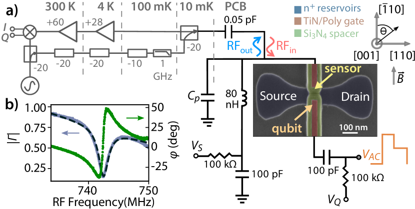
By monitoring the phase of the reflected RF signal, while the sensor and qubit potentials and are swept, it is possible to map out charge transitions for the two quantum dots (see Fig. 2d for detail and Supplementary Fig. S4 for a full stability diagram). Because the reflectometry signal is a function of the tunnelling rate of the sensor dot to the reservoir, and this rate depends on the sensor dot occupancy, , it is not straightforward to assign an electron occupation for this dot Lundberg et al. . Nevertheless, is not central to the charge sensing we employ here. The number of electrons in the qubit dot, , can be measured using the inter-dot capacitive coupling with the sensor: each change in shifts the sensor dot electrochemical potential (see Fig. 2d) allowing us to ensure complete depletion in the qubit dot by reducing until no further shifts are observed by the sensor (see Fig. S4).
III Spin readout
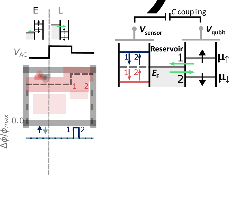
Once the qubit dot is depleted to its last electron, the spin degeneracy is lifted by applying a magnetic field in the plane of the device and perpendicular to the nanowire, in the crystallographic direction. The spin readout procedure follows a 3-level pulse applied to the gate forming the qubit dot, cycling between three states: ‘load’-‘empty’-‘read’ marked as ‘L’, ‘E’ and ‘R’, respectively in Fig. 2a. The potential of the ‘read’ state sits between ‘load’ and ‘empty’, at the charge transition for , such that Fermi energy of the reservoir lies between the Zeeman-split spin and states Elzerman et al. (2004). At this point, a spin electron remains in the qubit dot, while a spin electron tunnels out to the reservoir, to be subsequently replaced by a spin electron tunnelling on the qubit dot. This spin-dependent tunnelling is detected using the sensor dot when tuned to a point in the stability diagram where the reflectometry signal depends on the qubit dot electron occupation. Useable ‘read’ points in the stability diagram are ones where the charge transition intersects with the transition that yields a reflectometry signal. Two such points can be identified in Fig. 2d labelled ‘AR’ and ‘BR’. At ‘BR’, a reflectometry signal (arising from the transition) is visible only when the qubit dot is empty (). In this case, the signature of a spin electron on the qubit dot is the brief emergence of a reflectometry signal at the read point, as the electron tunnels out of the dot (and a new spin tunnels in). Conversely, at ‘AR’, a reflectometry signal is visible only when the qubit dot is occupied (), in which case the signature of spin is a transient reduction in the signal. Experiments on device B used point BR for readout, while those on device A used a point equivalent to AR in the device A stability diagram. Fig. 2c shows the ideal and measured spin readout traces averaged over 1024 ‘ELR’ cycles at both ‘AR’ and ‘BR’. Further tests of spin readout are shown in Supplementary §IV.
Detecting the spin-dependent transient signals requires that the tunneling rate between the qubit dot and reservoir falls within the resonator bandwidth. The resonator Q-factor in our experiments was magnetic field-dependent leading to a detection bandwidth in the range 1.4–5.0 MHz. Dot-to-reservoir tunnelling rates in these devices can be tuned by applying a voltage to a global metal top-gate (not shown in Fig. 1a) or to the substrate Ibberson et al. (2018); Ansaloni et al. . We applied 0 V and V to the metal top gate for Devices A and B respectively, with the substrate at 0V, to achieve suitably low tunnelling rates: MHz for device A and MHz for device B. The spin readout signal was further optimised by fine-tuning the sensor and qubit gate voltages and . Through simulations of the signal dependence on these voltages, arising from the energy-dependent tunnelling rates (see Eq. 1 and Supplementary §III, we obtain the tunnelling rates quoted above, as well as (for device B) an estimated g-factor of , and the qubit dot effective temperature of mK. This temperature limits the minimum Zeeman splitting (and hence magnetic field) at which spin readout is feasible and its elevation compared to the device temperature ( mK) is attributed to the influence of the rf readout signal applied to the sensor dot acting on the qubit dot. The rf power used for readout can be decreased, albeit with a reduction in the spin-up visibility (see Supplementary §VI), however, amplifiers operating at the quantum limit of introduced noise can be used to achieve higher sensitivity in RF reflectometry while using lower drive powers Schaal et al. (2020).
IV Spin relaxation
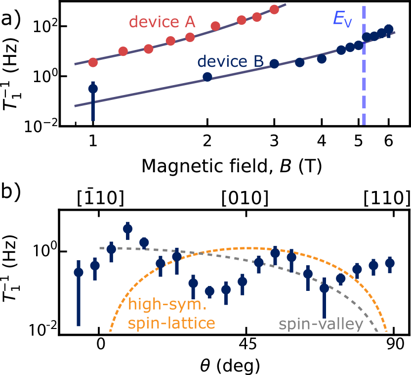
We next consider the effect of spin relaxation by varying the duration of the ‘load’ period in the 3-level pulse sequence. The spin of the loaded electron relaxes from its initial randomised state into the spin ground state with a time constant . We observe exponential decays in the spin fraction (see Supplementary §VIII) which we fit to obtain relaxation rates , plotted in Fig. 3 as a function of magnetic field strength and orientation. In both devices, we observe an increase in as the magnetic field in decreased up to a maximum of s (device A) and (device B) at T.
The magnetic field dependence of varies according to the relaxation mechanism and the direction of the field with respect to crystal axes. For the measurements presented in Fig. 3a the magnetic field was parallel to . Spin relaxation may arise from magnetic noise at the spin Zeeman frequency or, more commonly and given some spin-orbit coupling (SOC) that mixes the spin degree of freedom with orbital or valley states, from phonon-induced electric field noise or Johnson noise. At this field orientation, and far from any anti-crossing with higher-lying excited states Yang et al. (2013), the primary contributions from phonons to the relaxation rate -1 are proportional to Tahan and Joynt (2014a); Bourdet and Niquet (2018), while those from Johnson Nyquist noise are proportional to Tahan and Joynt (2014a). We therefore fit the data in Fig. 3a to a combination of such processes: (see Supplementary §IX).
We studied the angular dependence of the spin relaxation rate in device B, rotating a 1 T field in the plane of the device. A minimum in the relaxation rate is seen as the magnetic field is parallel to the direction of the nanowire, aligned along the [110] crystallographic direction. Such a minimum is expected as there is no spin-valley mixing (a typically dominant spin-orbit mixing mechanism) when the magnetic field is perpendicular to a mirror symmetry plane of the device Corna et al. (2018); Bourdet and Niquet (2018). However, we find that the usual models for spin-orbit driven relaxation Tahan and Joynt (2014b); Scarlino et al. (2014); Bourdet and Niquet (2018); Glavin and Kim (2003) (see dashed lines in Fig. 3b) are not able to account for all features in the angular dependence. In general though, spin-lattice relaxation can produce higher order harmonics in the dependence on magnetic field orientation, especially in quantum dots with high in-plane symmetry (see Supplementary §IX). Such a high symmetry would also suggest a weak spin-valley mixing, with implications on the relaxation behaviour when then Zeeman splitting becomes comparable to the excited state valley splitting.
V Excited state spectroscopy
To gain further insights into the spin relaxation mechanism for this device, we move on to study the excited valley states of this quantum dot by sweeping the voltage of the ‘load’ stage, . The rate at which an electron loads from the reservoir into some dot state depends on the difference in electrochemical potential, , between and the reservoir Fermi energy. Here, we consider four dot states, , where and are respectively the ground and excited -valley states, each with spin-up and spin-down states. Assuming elastic tunnelling and a constant reservoir density of states, the loading rate follows a Fermi-Dirac distribution centred at , when dot and lead potentials are aligned MacLean et al. (2007); Amasha et al. (2008):
| (1) |
where is the natural tunnel rate for each state , is the Boltzmann constant and the effective temperature. We assume here that the natural tunnel rates are spin-independent (i.e. for the ground states and they are equal to , and similarly for the excited state natural tunnel rate ), as well as independent of over the small ( mV) range of voltages studied here. The energy separation can be tuned with as , where is the voltage at which the dot state and reservoir potential align and is the gate lever arm of the ‘qubit gate’ to the qubit dot. From Eq. 1, tunnelling rates tend to zero for load voltages smaller than , and towards the natural tunnelling rate, , for higher voltages. As a result, varying the ‘load’ voltage changes the tunnelling rates into the various dot states, and thus the probability of loading a spin-up, which we detect using the spin-readout described above.
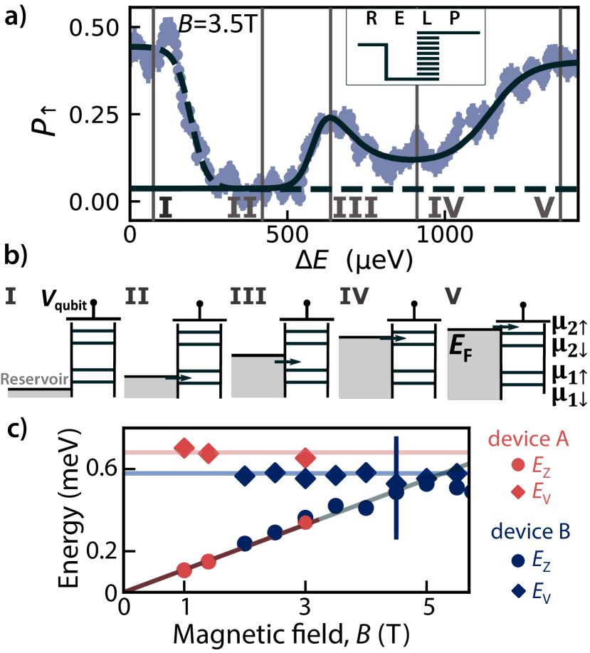
To perform excited state spectroscopy on the qubit dot we use a 4-level pulse-sequence (‘empty’-‘load’-‘plunge’-‘read’) applied to the qubit dot gate Morello et al. (2010), where the additional ‘plunge’ stage ensures that an electron is always loaded for any cycle, while the loading voltage is swept between the ‘empty’ and ‘plunge’ levels (see inset in Fig. 4a). We define a spin-up fraction based on the integrated spin-up signal, baseline-corrected, and normalised to obtain in the limit of zero load time (to neglect relaxation) and random loading using only the ‘plunge’ phase. The dependence of on the ‘load’ voltage (converted to energy) is shown in Fig. 4a, and can be understood by considering the schematics in Fig. 4b. In the limit (I) of low , no electron tunnels into the qubit dot during the ‘load’ phase and an electron of random spin is loaded during ‘plunge’. When the Fermi energy, , of the reservoir lies between the spin-up and spin-down states (II), only spin-down electrons tunnel into the dot, and drops to zero. Assuming the duration of the ‘load’ period in the pulse sequence is long compared to the natural tunnelling rates , the transition between regions I and II is characterised by the spin-down ground state loading rate, :
| (2) |
used to generate dashed curve in Fig. 4a.
As the ‘load’ voltage is further increased (III), both spin states can be loaded and the measured spin-up fraction increases. Excited states can also be measured in this way provided their decay rates to the ground state are sufficiently high Friesen et al. (2004); Tahan and Joynt (2014a). Once the spin-down excited state becomes available during the load process (IV), the measured spin-up fraction again reduces, since the excited state rapidly decays in a spin-conserving manner Simmons et al. (2011). Finally, in region (V), an electron of either spin orientation can be loaded into the excited state. In regions II–V, the measured spin up fraction can be modelled by combining all relevant rates Simmons et al. (2011):
| (3) |
By fitting the data to Eq. 3 (see solid line in Fig.4a) we can extract several parameters: i) The Zeeman splitting between the spin-up and spin-down states (fixed to be constant for the ground and excited valley states), related to the width of regions II and IV; ii) The valley splitting , related to the separation of regions II and IV; iii) The ratio between ground and excited state natural tunnelling rates, , related to the amplitude in region IV; and iv) the effective temperature , related to the sharpness of transitions between various regions (which can be seen to be different for the ground and excited states, as discussed further in Supplementary §VII).
Extracted values for and for both devices are shown in Fig. 4c as a function of magnetic field. As expected, shows a linear dependence with field with a g-factor of 1.91(10), while is field-independent and measured to be 0.68(2) meV (device A) and 0.57(3) meV (device B). These values are broadly similar (within a factor of two) to those measured in similar nanowire devices Urdampilleta et al. (2019) — furthermore, a large valley splitting is beneficial for spin qubits to remain within the computational basis states and maximise spin relaxation times Hollmann et al. (2020). The valley splitting in device B is shown as an equivalent magnetic field in Fig. 3, confirming the lack of an evident relaxation ‘hot-spot’ Yang et al. (2013); Petit et al. (2018); Borjans et al. (2019) where when there is a finite inter-valley spin-orbit matrix element leading to spin-valley mixing. A possible explanation for this absence is that the corner dot has greater symmetry than expected, with two orthogonal quasi-symmetry planes, thus weakening spin-valley mixing Corna et al. (2018) — this would be consistent with the complex magnetic field-orientation dependence of discussed above. Another possible explanation is phase cancellations between the valley coupling and spin-orbit coupling matrix elements strongly suppressing spin-valley mixing Nestoklon et al. (2006); Veldhorst et al. (2015b). In both cases, this interesting regime warrants investigation of further devices to ascertain the relationship between these conditions and the device geometry, growth conditions, and electrostatic environment.
VI Conclusions and Outlook
We have demonstrated time-averaged readout of a single spin confined in a CMOS quantum dot, using a nanowire device fabricated at the 300 mm wafer scale. We introduce a spin-readout method based on spin-dependent tunnelling combined with gate-based reflectometry of a neighbouring quantum dot to act as a charge sensor, representing a low-footprint approach to spin readout in silicon devices.
Our detector bandwidth and tunnel coupling of the sensor dot to the reservoir would permit spin readout on the timescale of 10 µs. However, further improvements in the signal-to-noise ratio (SNR) of the gate-based reflectometry are required to achieve high-fidelity single-shot measurements in such short times Keith et al. (2019); Connors et al. (2020); House et al. (2016). For a charge transition in the sensor dot, we measure an SNR of 1 for an integration time of 50 µs. The magnitude of the signal increases quadratically with the gate lever arm to the sensor dot Gonzalez-Zalba et al. (2015). Based on the values in our device ( and ) and similar asymmetries reported for nominally identical devices Lundberg et al. ; Ibberson et al. , SNR power could be increased by 16 simply by swapping the assignment of sensor and qubit.
Further improvements in SNR power (20 and 16 respectively) can be expected by further optimising the resonator design to detect capacitance changes Ibberson et al. and by lowering the noise floor through use of a quantum-limited amplifier Schaal et al. (2020). Combining these methods, improvements in SNR power of three orders of magnitude are possible, bringing single-shot readout well within reach while simultaneously reducing the RF power used for readout to avoid limiting the minimum measurable Zeeman splitting.
These split-gate nanowire devices can be naturally scaled to produce 2x arrays of corner quantum dots Hutin et al. (2019); Chanrion et al. — such devices could represent a 1D spin qubit array along one edge of the nanowire, where end qubits have charge sensors used for readout based on the approach presented here. 1D qubit arrays are well-suited for certain quantum simulation problems, such as a variational quantum eigensolver approach to the Hubbard model Cai (2019); Cade et al. . Spin shuttling Fujita et al. (2017) or qubit SWAPping Sigillito et al. (2019) could transport qubits to the ends of the array, however, for some algorithms readout of an end-qubit ancilla is sufficient Yuan et al. (2019).
While it is the spin coherence time which ultimately limits qubit fidelity, the long spin relaxation times we measure (up to 9 s) is particularly encouraging for these devices. These indicate that both the CMOS-compatible fabrication methods and the nanowire geometry with its corner quantum dots are all consistent with large valley splittings and long spin relaxation times, making them an attractive platform for scalable quantum computing.
Acknowledgements.
We acknowledge the financial support from the European Union’s Horizon 2020 research and innovation programme under grant agreement No 688539 (http://mos-quito.eu); as well as the UK’s Engineering and Physical Sciences Research Council (EPSRC) through the Centre for Doctoral Training in Delivering Quantum Technologies (EP/L015242/1), QUES2T (EP/N015118/1) and the Hub in Quantum Computing and Simulation (EP/T001062/1). V.N.C.T. acknowledges the support from the Telefónica British-Spanish society scholarship. ”Y.-M.N. and J.L. acknowledge support from the French national research agency (ANR project MAQSi). M.F.G.Z. acknowledges support from the Royal Society.References
- Loss and DiVincenzo (1998) D. Loss and D. P. DiVincenzo, Quantum computation with quantum dots, Phys. Rev. A 57, 120 (1998).
- Yoneda et al. (2018) J. Yoneda, K. Takeda, T. Otsuka, T. Nakajima, M. R. Delbecq, G. Allison, T. Honda, T. Kodera, S. Oda, Y. Hoshi, N. Usami, K. M. Itoh, and S. Tarucha, A quantum-dot spin qubit with coherence limited by charge noise and fidelity higher than 99.9%, Nat. Nanotechnol. 13, 102 (2018).
- Urdampilleta et al. (2019) M. Urdampilleta, D. J. Niegemann, E. Chanrion, B. Jadot, C. Spence, P. A. Mortemousque, C. Bäuerle, L. Hutin, B. Bertrand, S. Barraud, R. Maurand, M. Sanquer, X. Jehl, S. De Franceschi, M. Vinet, and T. Meunier, Gate-based high fidelity spin readout in a CMOS device, Nat. Nanotechnol. 14, 737 (2019).
- Connors et al. (2020) E. J. Connors, JJ Nelson, and J. M. Nichol, Rapid High-Fidelity Spin-State Readout in Si/Si-Ge Quantum Dots via rf Reflectometry, Phys. Rev. Appl. 13, 024019 (2020).
- Yoneda et al. (2020) J. Yoneda, K. Takeda, A. Noiri, T. Nakajima, S. Li, J. Kamioka, T. Kodera, and S. Tarucha, Quantum non-demolition readout of an electron spin in silicon, Nat. Commun. 11, 1144 (2020).
- Veldhorst et al. (2014) M. Veldhorst, J. C. C. Hwang, C. H. Yang, A. W. Leenstra, B. De Ronde, J. P. Dehollain, J. T. Muhonen, F. E. Hudson, K. M. Itoh, A. Morello, and A. S. Dzurak, An addressable quantum dot qubit with fault-tolerant control-fidelity, Nat. Nanotechnol. 9, 981 (2014).
- Kawakami et al. (2014) E. Kawakami, P. Scarlino, D. R. Ward, F. R. Braakman, D. E. Savage, M. G. Lagally, M. Friesen, S. N. Coppersmith, M. A. Eriksson, and L. M. K Vandersypen, Electrical control of a long-lived spin qubit in a Si/SiGe quantum dot, Nat. Nanotechnol. 9, 666 (2014).
- Veldhorst et al. (2015a) M. Veldhorst, C. H. Yang, J. C. C. Hwang, W. Huang, J. P. Dehollain, J. T. Muhonen, S. Simmons, A. Laucht, F. E. Hudson, K. M. Itoh, A. Morello, and A. S. Dzurak, A two-qubit logic gate in silicon, Nature 526, 410 (2015a).
- Zajac et al. (2018) D. M. Zajac, A. J. Sigillito, M. Russ, F. Borjans, J. M. Taylor, G. Burkard, and J. R. Petta, Resonantly driven CNOT gate for electron spins, Science 359, 439 (2018).
- Watson et al. (2018) T. F. Watson, S. G. Philips, E. Kawakami, D. R. Ward, P. Scarlino, M. Veldhorst, D. E. Savage, M. G. Lagally, M. Friesen, S. N. Coppersmith, M. A. Eriksson, and L. M. K Vandersypen, A programmable two-qubit quantum processor in silicon, Nature 555, 633 (2018).
- Xue et al. (2019) X. Xue, T. F. Watson, J. Helsen, D. R. Ward, D. E. Savage, M. G. Lagally, S. N. Coppersmith, M. A. Eriksson, S. Wehner, and L. M. K Vandersypen, Benchmarking Gate Fidelities in a Si/SiGe Two-Qubit Device, Phys. Rev. X 9, 021011 (2019).
- Maurand et al. (2016) R. Maurand, X. Jehl, D. Kotekar-Patil, A. Corna, H. Bohuslavskyi, R. Laviéville, L. Hutin, S. Barraud, M. Vinet, M. Sanquer, and S. De Franceschi, A CMOS silicon spin qubit., Nat. Commun. 7, 13575 (2016).
- Ono et al. (2002) K. Ono, D. Austing, Y. Tokura, and S. Tarucha, Current rectification by pauli exclusion in a weakly coupled double quantum dot system, Science 297, 1313 (2002).
- Elzerman et al. (2004) J. M. Elzerman, R. Hanson, L. H. Van Beveren, B. Witkamp, L. M. K Vandersypen, and L. P. Kouwenhoven, Single-shot read-out of an individual electron spin in a quantum dot, Nature 430, 431 (2004).
- West et al. (2019) A. West, B. Hensen, A. Jouan, T. Tanttu, C. H. Yang, A. Rossi, M. F. Gonzalez-Zalba, F. E. Hudson, A. Morello, D. J. Reilly, and A. S. Dzurak, Gate-based single-shot readout of spins in silicon, Nat. Nanotechnol. 14, 437 (2019).
- Zheng et al. (2019) G. Zheng, N. Samkharadze, M. L. Noordam, N. Kalhor, D. Brousse, A. Sammak, G. Scappucci, and L. M. K Vandersypen, Rapid gate-based spin read-out in silicon using an on-chip resonator, Nat. Nanotechnol. 14, 742 (2019).
- Pakkiam et al. (2018) P. Pakkiam, A. V. Timofeev, M. G. House, M. R. Hogg, T. Kobayashi, M. Koch, S. Rogge, and M. Y. Simmons, Single-Shot Single-Gate rf Spin Readout in Silicon, Phys. Rev. X 8, 41032 (2018).
- Morello et al. (2010) A. Morello, J. J. Pla, F. A. Zwanenburg, K. W. Chan, K. Y. Tan, H. Huebl, M. Mottonen, C. D. Nugroho, C. Yang, J. A. Van Donkelaar, A. D. Alves, D. N. Jamieson, C. C. Escott, L. C. Hollenberg, R. G. Clark, and A. S. Dzurak, Single-shot readout of an electron spin in silicon, Nature 467, 687 (2010).
- Watson et al. (2015) T. F. Watson, B. Weber, M. G. House, H. Büch, and M. Y. Simmons, High-Fidelity Rapid Initialization and Read-Out of an Electron Spin via the Single Donor D- Charge State, Phys. Rev. Lett. 115, 166806 (2015).
- Fogarty et al. (2018) M. Fogarty, K. Chan, B. Hensen, W. Huang, T. Tanttu, C. Yang, A. Laucht, M. Veldhorst, F. E. Hudson, K. M. Itoh, et al., Integrated silicon qubit platform with single-spin addressability, exchange control and single-shot singlet-triplet readout, Nat. Commun. 9, 4370 (2018).
- Zhao et al. (2019) R. Zhao, T. Tanttu, K. Y. Tan, B. Hensen, K. W. Chan, J. C. C. Hwang, R. Leon, C. H. Yang, W. Gilbert, F. E. Hudson, et al., Single-spin qubits in isotopically enriched silicon at low magnetic field, Nat. Commun. 10, 5500 (2019).
- Harvey-Collard et al. (2018) P. Harvey-Collard, B. D’Anjou, M. Rudolph, N. T. Jacobson, J. Dominguez, G. A. Ten Eyck, J. R. Wendt, T. Pluym, M. P. Lilly, W. A. Coish, M. Pioro-Ladrière, and M. S. Carroll, High-Fidelity Single-Shot Readout for a Spin Qubit via an Enhanced Latching Mechanism, Phys. Rev. X 8, 021046 (2018).
- Curry et al. (2019) M. J. Curry, M. Rudolph, T. England, A. Mounce, R. Jock, C. Bureau-Oxton, P. Harvey-Collard, P. Sharma, J. Anderson, D. Campbell, et al., Single-shot readout performance of two heterojunction-bipolar-transistor amplification circuits at millikelvin temperatures, Sci. Rep 9, 16976 (2019).
- House et al. (2016) M. G. House, I. Bartlett, P. Pakkiam, M. Koch, E. Peretz, J. Van Der Heijden, T. Kobayashi, S. Rogge, and M. Y. Simmons, High-Sensitivity Charge Detection with a Single-Lead Quantum Dot for Scalable Quantum Computation, Phys. Rev. Appl. 6, 044016 (2016).
- (25) E. Chanrion, D. J. Niegemann, B. Bertrand, C. Spence, B. Jadot, J. Li, P.-A. Mortemousque, L. Hutin, R. Maurand, X. Jehl, M. Sanquer, S. De Franceschi, C. B äuerle, F. Balestro, Y.-M. Niquet, M. Vinet, T. Meunier, and M. Urdampilleta, Charge detection in an array of CMOS quantum dots, arXiv:2004.01009 .
- (26) F. Ansaloni, A. Chatterjee, H. Bohuslavskyi, B. Bertrand, L. Hutin, M. Vinet, and F. Kuemmeth, Single-electron control in a foundry-fabricated two-dimensional qubit array, arXiv:2004.00894 .
- Persson et al. (2010) F. Persson, C. M. Wilson, M. Sandberg, G. Johansson, and P. Delsing, Excess Dissipation in a Single-Electron Box: The Sisyphus Resistance, Nano Lett. 10, 953 (2010).
- Gonzalez-Zalba et al. (2015) M. F. Gonzalez-Zalba, S. Barraud, A. J. Ferguson, and A. C. Betz, Probing the limits of gate-based charge sensing, Nat. Commun. 6, 6084 (2015).
- Voisin et al. (2014) B. Voisin, V. H. Nguyen, J. Renard, X. Jehl, S. Barraud, F. Triozon, M. Vinet, I. Duchemin, Y. M. Niquet, S. De Franceschi, and M. Sanquer, Few-electron edge-state quantum dots in a silicon nanowire field-effect transistor, Nano Lett. 14, 2094 (2014).
- Ahmed et al. (2018) I. Ahmed, J. A. Haigh, S. Schaal, S. Barraud, Y. Zhu, C. M. Lee, M. Amado, J. W. A. Robinson, A. Rossi, J. J. L. Morton, and M. F. Gonzalez-Zalba, Radio-Frequency Capacitive Gate-Based Sensing, Phys. Rev. Appl. 10, 014018 (2018).
- (31) T. Lundberg, J. Li, L. Hutin, B. Bertrand, D. J. Ibberson, C.-M. Lee, D. J. Niegemann, M. Urdampilleta, N. Stelmashenko, T. Meunier, J. W. A. Robinson, L. Ibberson, M. Vinet, Y. M. Niquet, and M. F. Gonzalez-Zalba, A Spin Quintet in a Silicon Double Quantum Dot: Spin Blockade and Relaxation, arXiv:1910.10118 .
- Ibberson et al. (2018) D. J. Ibberson, L. Bourdet, J. C. Abadillo-Uriel, I. Ahmed, S. Barraud, M. J. Calderón, Y. M. Niquet, and M. F. Gonzalez-Zalba, Electric-field tuning of the valley splitting in silicon corner dots, Appl. Phys. Lett. 113, 053104 (2018).
- Schaal et al. (2020) S. Schaal, I. Ahmed, J. A. Haigh, L. Hutin, B. Bertrand, S. Barraud, M. Vinet, C.-M. Lee, N. Stelmashenko, J. W. A. Robinson, J. Y. Qiu, S. Hacohen-Gourgy, I. Siddiqi, M. F. Gonzalez-Zalba, and J. J. L. Morton, Fast Gate-Based Readout of Silicon Quantum Dots Using Josephson Parametric Amplification, Phys. Rev. Lett. 124, 67701 (2020).
- Glavin and Kim (2003) B. A. Glavin and K. W. Kim, Spin-lattice relaxation in Si quantum dots, Phys. Rev. B 68, 045308 (2003).
- Yang et al. (2013) C. H. Yang, A. Rossi, R. Ruskov, N. S. Lai, F. A. Mohiyaddin, S. Lee, C. Tahan, G. Klimeck, A. Morello, and A. S. Dzurak, Spin-valley lifetimes in a silicon quantum dot with tunable valley splitting, Nat. Commun. 4, 2069 (2013).
- Tahan and Joynt (2014a) C. Tahan and R. Joynt, Relaxation of excited spin, orbital, and valley qubit states in ideal silicon quantum dots, Phys. Rev. B 89, 075302 (2014a).
- Bourdet and Niquet (2018) L. Bourdet and Y. M. Niquet, All-electrical manipulation of silicon spin qubits with tunable spin-valley mixing, Phys. Rev. B 97, 155433 (2018).
- Corna et al. (2018) A. Corna, L. Bourdet, R. Maurand, A. Crippa, D. Kotekar-Patil, H. Bohuslavskyi, R. Laviéville, L. Hutin, S. Barraud, X. Jehl, M. Vinet, S. De Franceschi, Y. M. Niquet, and M. Sanquer, Electrically driven electron spin resonance mediated by spin-valley-orbit coupling in a silicon quantum dot, npj Quantum Inf. 4, 6 (2018).
- Tahan and Joynt (2014b) C. Tahan and R. Joynt, Relaxation of excited spin, orbital, and valley qubit states in ideal silicon quantum dots, Phys. Rev. B 89, 075302 (2014b).
- Scarlino et al. (2014) P. Scarlino, E. Kawakami, P. Stano, M. Shafiei, C. Reichl, W. Wegscheider, and L. M. K. Vandersypen, Spin-relaxation anisotropy in a GaAs quantum dot, Phys. Rev. Lett. 113, 256802 (2014).
- MacLean et al. (2007) K. MacLean, S. Amasha, I. P. Radu, D. M. Zumbühl, M. A. Kastner, M. P. Hanson, and A. C. Gossard, Energy-dependent tunneling in a quantum dot, Phys. Rev. Lett. 98, 036802 (2007).
- Amasha et al. (2008) S. Amasha, K. MacLean, I. P. Radu, D. M. Zumbühl, M. A. Kastner, M. P. Hanson, and A. C. Gossard, Spin-dependent tunneling of single electrons into an empty quantum dot, Phys. Rev. B 78, 041306(R) (2008).
- Friesen et al. (2004) M. Friesen, C. Tahan, R. Joynt, and M. A. Eriksson, Spin Readout and Initialization in a Semiconductor Quantum Dot, Phys. Rev. Lett. 92, 037901 (2004).
- Simmons et al. (2011) C. B. Simmons, J. R. Prance, B. J. Van Bael, T. S. Koh, Z. Shi, D. E. Savage, M. G. Lagally, R. Joynt, M. Friesen, S. N. Coppersmith, and M. A. Eriksson, Tunable spin loading and T1 of a silicon spin qubit measured by single-shot readout, Phys. Rev. Lett. 106, 156804 (2011).
- Hollmann et al. (2020) A. Hollmann, T. Struck, V. Langrock, A. Schmidbauer, F. Schauer, T. Leonhardt, K. Sawano, H. Riemann, N. V. Abrosimov, D. Bougeard, and L. R. Schreiber, Large, Tunable Valley Splitting and Single-Spin Relaxation Mechanisms in a Quantum Dot, Phys. Rev. Appl. 13, 034068 (2020).
- Petit et al. (2018) L. Petit, J. M. Boter, H. G. J. Eenink, G. Droulers, M. L. V. Tagliaferri, R. Li, D. P. Franke, K. J. Singh, J. S. Clarke, R. N. Schouten, V. V. Dobrovitski, L. M. K Vandersypen, and M. Veldhorst, Spin Lifetime and Charge Noise in Hot Silicon Quantum Dot Qubits, Phys. Rev. Lett. 121, 076801 (2018).
- Borjans et al. (2019) F. Borjans, D. M. Zajac, T. M. Hazard, and J. R. Petta, Single-Spin Relaxation in a Synthetic Spin-Orbit Field, Phys. Rev. Appl. 11, 044063 (2019).
- Nestoklon et al. (2006) M. O. Nestoklon, L. E. Golub, and E. L. Ivchenko, Spin and valley-orbit splittings in heterostructures, Phys. Rev. B 73, 235334 (2006).
- Veldhorst et al. (2015b) M. Veldhorst, R. Ruskov, C. H. Yang, J. C. C. Hwang, F. E. Hudson, M. E. Flatté, C. Tahan, K. M. Itoh, A. Morello, and A. S. Dzurak, Spin-orbit coupling and operation of multivalley spin qubits, Phys. Rev. B 92, 201401(R) (2015b).
- Keith et al. (2019) D. Keith, M. G. House, M. B. Donnelly, T. F. Watson, B. Weber, and M. Y. Simmons, Single-Shot Spin Readout in Semiconductors Near the Shot-Noise Sensitivity Limit, Phys. Rev. X 9, 41003 (2019).
- (51) D. J. Ibberson, T. Lundberg, J. A. Haigh, L. Hutin, B. Bertrand, S. Barraud, C.-M. Lee, N. A. Stelmashenko, J. W. A. Robinson, M. Vinet, M. F. Gonzalez-Zalba, and L. A. Ibberson, Large dispersive interaction between a CMOS double quantum dot and microwave photons, arXiv:2004.00334 .
- Hutin et al. (2019) L. Hutin, B. Bertrand, E. Chanrion, H. Bohuslavskyi, F. Ansaloni, T. . Yang, J. Michniewicz, D. J. Niegemann, C. Spence, T. Lundberg, A. Chatterjee, A. Crippa, J. Li, R. Maurand, X. Jehl, M. Sanquer, M. F. Gonzalez-Zalba, F. Kuemmeth, Y. . Niquet, S. De Franceschi, M. Urdampilleta, T. Meunier, and M. Vinet, Gate reflectometry for probing charge and spin states in linear si mos split-gate arrays, in 2019 IEEE International Electron Devices Meeting (IEDM) (2019) pp. 37.7.1–37.7.4.
- Cai (2019) Z. Cai, Resource Estimation for Quantum Variational Simulations of the Hubbard Model: The Advantage of Multi-core NISQ Processing, arXiv:1910.02719 .
- (54) C. Cade, L. Mineh, A. Montanaro, and S. Stanisic, Strategies for solving the Fermi-Hubbard model on near-term quantum computers, arXiv:1912.06007 .
- Fujita et al. (2017) T. Fujita, T. A. Baart, C. Reichl, W. Wegscheider, and L. M. K. Vandersypen, Coherent shuttle of electron-spin states, npj Quantum Inf. 3, 22 (2017).
- Sigillito et al. (2019) A. J. Sigillito, M. J. Gullans, L. F. Edge, M. Borselli, and J. R. Petta, Coherent transfer of quantum information in a silicon double quantum dot using resonant SWAP gates, npj Quantum Inf. 5, 110 (2019).
- Yuan et al. (2019) X. Yuan, S. Endo, Q. Zhao, Y. Li, and S. C. Benjamin, Theory of variational quantum simulation, Quantum 3, 191 (2019).