Spectral and spatial isolation of single WSe2 quantum emitters using hexagonal boron nitride wrinkles
Abstract
Monolayer WSe2 hosts bright single-photon emitters. Because of its compliance, monolayer WSe2 conforms to patterned substrates without breaking, thus creating the potential for large local strain, which is one activation mechanism of its intrinsic quantum emitters. Here, we report an approach to creating spatially and spectrally isolated quantum emitters from WSe2 monolayers with few or no detrimental sources of emission. We show that a bilayer of hexagonal boron nitride (hBN) and WSe2 placed on a nanostructured substrate can be used to create and shape wrinkles that communicate local strain to the WSe2 , thus creating quantum emitters that are isolated from substrate features. We compare quantum emitters created directly on top of substrate features with quantum emitters forming along wrinkles and find that the spectra of the latter consist of mainly a single peak and a low background fluorescence. We also discuss possible approaches to controlling emitter position along hBN wrinkles.
Solid-state quantum emitters (QEs) such as semiconductor quantum dots and color centers in solids have promising applications in quantum information science, optoelectronics and nano-sensing because of their versatility, stability and sensitivity O’Brien, Furusawa, and Vučković (2009); Gisin et al. (2002); Kimble (2008); Aharonovich, Englund, and Toth (2016). Monolayer transition metal dichalcogenides (TMDs) are direct bandgap semiconductors with strong light-matter interactions, large excitonic effects and a valley degree of freedom that locks excitons to a given photon helicity Mak and Shan (2016). Quantum emitters in TMDs that inherit valley properties could be used for the generation of single photons with orthogonal polarization for polarization-encoded flying qubits Schaibley et al. (2016). One TMD, tungsten diselenide (WSe2), hosts bright and stable QEs Srivastava et al. (2015); He et al. (2015); Koperski et al. (2015); Chakraborty et al. (2015), which have been used in a broad range of experiments that shows their potential: fine-structure splitting manipulation with electric field Chakraborty et al. (2019), linear-to-circular helicity conversion with magnetic field He et al. (2015), quantum confined Stark tuning of excitons Chakraborty et al. (2017), and single charge injection to trion state Chakraborty et al. (2018); Brotons-Gisbert et al. (2019).
While most reported emitters in WSe2 monolayers are located at random, a few reports demonstrate quasi-deterministic activation of QEs via local strain by placing the WSe2 monolayer over a substrate patterned with nanopillars Branny et al. (2017); Palacios-Berraquero et al. (2017), a slotted waveguide Kern et al. (2016) or hexagonal boron nitride nano-bubbles Shepard et al. (2017). Based on these works, it has become clear that strain plays a role in activating WSe2 QEs, although their precise nature – whether excitonic or defect-bound Branny et al. (2017); Zheng et al. (2019) – is still being actively investigated. There is still no reliable method to strain-engineer single QEs in WSe2 deterministically. In most reports, the strain in WSe2 monolayers that is created at random or at a pillar apex is complex and non-uniform, resulting in the creation of multiple QEs per site. Eventually this results in the excitation and emission from several QEs at once leading to degraded single photon purity and the need for tunable spectral filtering of specific emitters.
Here, we report on an alternative approach to create spatially isolated single QEs in WSe2 monolayers with the help of hexagonal boron nitride (hBN). Unlike previous WSe2 QE studies involving hBN as an insulating layer in heterostructures including graphene Chakraborty et al. (2018, 2017, 2019), we use hBN as a strain buffer from a nanostructured substrate to control the amount of strain applied to WSe2. By stacking WSe2 with sub-10-nm hBN, wrinkles nucleate from a nanostructured substrate and create local strain in WSe2 at a spatial location away from the substrate pattern. We find that these wrinkle points frequently host a single QE with very low background. These two properties – number of QEs created per site and the peak-to-background ratio at the emitter frequency – are important figures-of-merit to quantify since spectral overlap from other emitters and background light on top of a QE of interest are intrinsically detrimental to the single-photon purity of the source. We extract a peak-to-background ratio as high as for wrinkle-based QEs with an average of for a 3 nm spectral width. In comparison, pillar-based QEs have an average peak-to-background ratio of due to the typical formation of a much richer spectrum composed of several emitter lines and a larger background. We also find that using a thin hBN capping layer above WSe2 reduces spectral wandering and blinking. Finally, we discuss approaches to controllably introduce local wrinkles in hBN in desired locations, thus enabling deterministic positioning of single WSe2 QEs. In this vein, we present a sample patterned in different designs to exemplify that many strain profiles are suitable to activate QEs and that nanopillars are not the obvious way to activate WSe2 QEs.
Nanopillar versus wrinkle-based quantum emitters
Strain engineering of WSe2 monolayers is a proven method for creating QEs on demand and with position control Branny et al. (2017); Palacios-Berraquero et al. (2017); Cai et al. (2018). Previous methods have employed WSe2 monolayers strained directly on top of a nano-patterned substrate to create QEs. Our approach uses a nano-patterned substrate as an indirect means to communicate strain to WSe2 via a thin hBN layer. By conforming to the uneven substrate, the thin hbN layer supports wrinkles and small height variations, which strains WSe2 differently than if WSe2 were to conform to the lithographically defined structures by itself. In the first part of this work, we use a substrate patterned with nanopillars following the fabrication recipe of Proscia et al. Proscia et al. (2018) and make a comparative study of emitters forming directly on the pillars versus along hBN wrinkles that propagate between pillars.
The nanopillars are fabricated from an SiO2(500 nm)/p-Si(500 µm) substrate via electron-beam lithography (JEOL 6300) using M-aN 2403 negative resist Proscia et al. (2018). The nanopillars (and other structures) are etched into SiO2 and are cylindrical with a diameter of 200 nm and height of 300 nm. The spacing between pillars is 4 µm, which we found is phenomenologically the minimum spacing that allows the WSe2/hBN stack to both conform to the pillars and adhere to the substrate via Van der Waals forces. To place an exfoliated WSe2 monolayer deterministically over the fabricated nanopillars, we employ a polycarbonate (PC) on polydimethylsiloxane (PDMS) stamp technique Wang et al. (2013), which is commonly used to make heterostructures of 2D materials. The PC is used to pick up WSe2 and hBN (or vice versa) successively and melted at 180 C on top of the target substrate. The melted PC is finally dissolved in chloroform for 10 minutes. The hBN/WSe2 stack is transferred such that the WSe2 monolayer is in contact with a Au electrode. A small bias of 1 V is applied accross the SiO2 layer between the WSe2 monolayer and the back silicon layer, which is used to passivate the electrostatic environment and stabilize QEs. In this section, we study two samples made from the same substrate: sample 1 contains a hBN(bottom)/WSe2 stack and sample 2 contains a WSe2/hBN(top) stack.
We study the samples using a homebuilt confocal microscope setup with a 637 nm continuous wave laser focused with a 50x Olympus () to the diffraction limit ( m). The sample is placed in a helium flow cryostat at 10 K. The laser light is filtered out in collection with a long-pass filter and sent onto silicon avalanche photodiodes (APDs) for time-resolved measurements or a spectrometer (Princeton Acton SP-2500) with focal length mm and a 300 g/mm grating. Single QE lines are filtered through a Semrock tunable filter with a 3 nm transmission bandwidth.
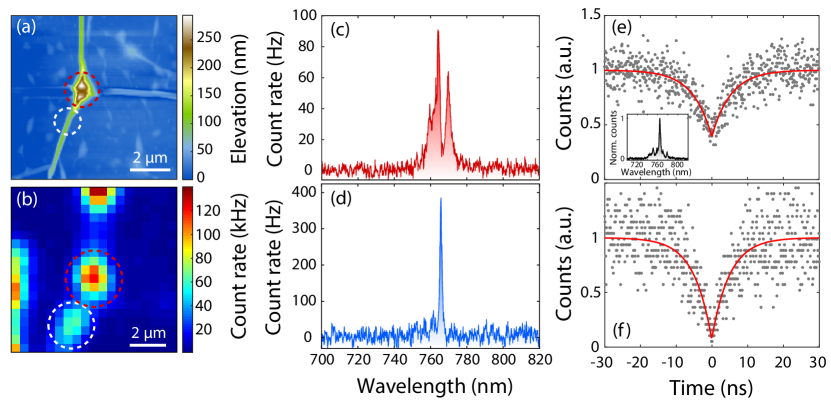
Previous studies using nanopillars to activate QEs show that WSe2 strained by a nanopillar apex become the brightest centers of photoluminescence on the monolayer Kumar, Kaczmarczyk, and Gerardot (2015); Palacios-Berraquero et al. (2017); Branny et al. (2017). The spectra associated with these bright spots are composed of several sharp lines and a broad background of weakly bound excitons (720-780 nm). In this present work, we are able to reproduce similar results when we study the bright emission centers directly on top of nanopillars. Most remarkably, we identify that one emission center along a hBN wrinkle corresponds to a single QE with low surrounding background emission. Figure 1(a) plots an atomic force microscopy (AFM) image of sample 1 consisting of a hBN/WSe2 heterostructure on a SiO2 nanopillar substrate. The photoluminescence (PL) map of this sample area obtained after exciting at 637 nm with 500 nW laser power is plotted in Fig. 1(b). The brightest emission is recorded on top of pillars (center and top of the image) and at the folded monolayer edge (left). A fluorescent spot is also visible along a hBN wrinkle, as indicated with a white dashed circle in Fig. 1(a-b). The spectrum from the center of the nanopillar is shown in Fig. 1(c) and features a broad emission peak from 755 nm to 775 nm, on top of which two peaks may be identified. Figure 1(d) shows a spectrum collected from the wrinkle shooting off the nanopillar (see white circle). This spectrum features a comparably single sharp peak at 765.8 nm with minimal background emission surrounding the peak. The AFM image reveals a kink in the wrinkle, which can explain the creation of a QE at this specific site. At this location, the wrinkle is 90 nm high and has a full-width at half-maximum (FWHM) of 160 nm. The collected light from this spot is filtered through a 3 nm bandpass filter and sent to a Hanbury-Brown-Twiss interferometer for auto-correlation measurement. The time correlation between the two APD signals for the wrinkle QE is plotted as in Fig. 1(f). The data is fitted with , where and is a characteristic time and amplitude of photon antibunching, respectively. From the fit we extract , unequivocally demonstrating the single-photon nature of the emission. Figure 1(e) shows the of a filtered QE collected from a pillar (spectrum shown as inset), from which we extract . The detrimental effect of spectral proximity to other emitters and background emission collected with the QE clearly impacts the single-photon purity. In the following section, we quantify the amount of unwanted background emission associated with several QEs. This sample provides a first insight into the difference in spectral quality between pillar and wrinkle QEs; an effect that we study extensively in the next sample where we observe reproducible behavior.
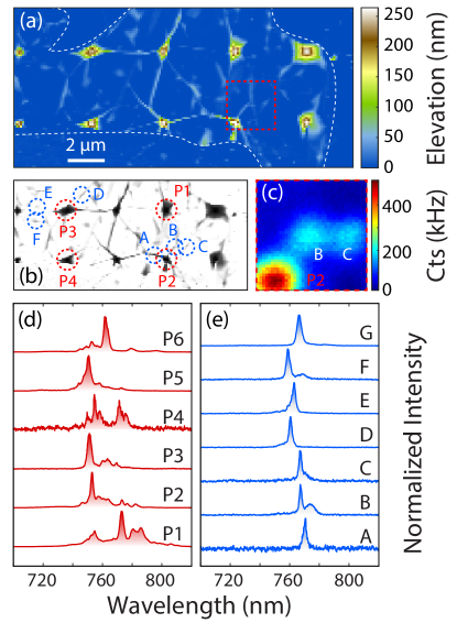
We now study sample 2 where the hBN layer is on top of WSe2 instead of the bottom. As in the previous case, single QEs are found on the pillars as well as between pillars where hBN forms wrinkles or nano-bubbles Shepard et al. (2017); Darlington et al. (2020). Figure 2(a) shows an AFM image of the sample where 6 nanopillars are investigated. All on-pillar and off-pillar emission centers are labeled in Fig. 2(b). Again, a PL-map – recorded from the area inside the red square box in Fig. 2(a) – shows that pillars emit the most light while there are other emission centers away from the pillars, see Fig. 2(c). We compare emission spectra of 6 on-pillar emitters and 7 off-pillar emitters in Figs. 2(d-e). The spectra collected from the top of the pillars show one or several lines attributed to QEs and a broad emission background. We quantify the peak-to-background ratio for a 3 nm spectral window, corresponding to our experimental conditions. To extract and , each spectra is fitted with the following function , where is proportional to the peak intensity, is the peak center wavelength, is the peak full-width at half maximum (FWHM) and is the wavelength-dependent background level. is computed as the integrated intensity of the peak and is the integrated , both of which limited to a 3 nm spectral window around the emitter center wavelength. For a graphical representation of how the ratio is extracted from a spectrum, refer to Fig. 6 in Appendix A. Quantum emitters stemming from pillars have an average of . That is, a fourth of the filtered emission comes from sources other than the single-photon source of interest. This background emission cannot be experimentally separated from the single photons and such sources will intrinsically have a low single-photon purity and limited applicability Gisin et al. (2002); Broome et al. (2013). In Fig. 2(e), we sample spectra that are collected along wrinkles that form away from the pillars. The spectra consistently display a single peak, i.e., a single QE probed at a time, while the background level is significantly reduced compared to the spectra of Fig. 2(b). The average for wrinkle-based QEs is , meaning one photon in eight comes from unwanted sources in the filtered signal, which is a 2 improvement. Four emitters out of seven (labeled A, E, F and G), have with the highest value being , all allowing for high single-photon purity. We speculate that the variation in is due to the different wrinkle sizes and morphology, which influence the confining potential and the presence of weakly bound excitons that contribute to background fluorescence. We also note that there are multiple instances in the literature that report spectrally isolated single quantum emitters, formed at random over a thick exfoliated hBN substrate Kumar et al. (2016) or from high aspect ratio nanopillars with sub-100 nm diameter Palacios-Berraquero et al. (2017).
The peak-to-background ratio estimation can be extended to the full spectrum as a way to probe the overall amount of background and other emitters collected in the signal along with the QE of interest. In practice, we compare a QE peak intensity to the sum of all pixels in the collected spectrum. On average, the main QE peak makes 60 % of the signal along wrinkles and 26 % on pillars. That is, for equal peak intensity, single photons from wrinkle-based QEs are collected with roughly 4 times as little unwanted emission in the unfiltered spectrum compared to pillar QEs. In the best case, we find that one wrinkle QE has a full-spectrum peak-to-background ratio of . Further improvement of this ratio could allow for direct use of the single-photon source without spectral filtering, which is currently a default setting for semiconductor sources Lodahl, Mahmoodian, and Stobbe (2015). A known way to clean a QE’s spectrum is to use quasi-resonant excitation, whereby the QE is excited through a higher energy state and other emitters do not respond to the same excitation energy Kumar et al. (2016). This requires a tunable laser close to the QE ground state energy and most often a cross-polarization excitation scheme.
Influence of Hexagonal boron nitride on the spectral stability of WSe2 quantum emitters

Another aspect that influences the applicability of single-photon sources is the emitter’s spectral and temporal stability. Spectral diffusion and blinking is commonly observed in all solid-state emitters because of fluctuations in the electrostatic environment. Such spectral instabilities are detrimental because they reduce the two-photon indistinguishability and overall excitation/collection efficiency with resonant excitation or spectral filtering Lodahl, Mahmoodian, and Stobbe (2015). Spectral wandering is commonly reported for WSe2 QEs on SiO2 substrates, however, blinking is seldom observed Srivastava et al. (2015); Chakraborty et al. (2015). Hexagonal boron nitride has been previously used with WSe2 as a buffer layer to isolate from the substrate Kumar et al. (2016), however the effect of the substrate on QE stability has not been fully understood. Tonndorf et al. Tonndorf et al. (2015) studied the effect of using hBN versus SiO2 substrates and found no clear influence on QE stability although hBN was found to increase non-radiative recombination channels. Substrate engineering with InGaP was also shown to yield WSe2 QEs with no detectable spectral diffusion Iff et al. (2017). For strain-activated QEs, pillars with a 2:1 aspect ratio (200 nm tall, 100 nm width) create less emitters per pillar with low spectral wandering and blinking whereas 1:1 aspect ratio pillars host more QEs, which tend to display substantial blinking and spectral diffusion over time Palacios-Berraquero et al. (2017).
In the process of working with hBN/WSe2 stacks on SiO2 substrates, we have also examined the effect of using an hBN passivation layer (hBN) on the spectral stability of QEs. Figure 3 shows a spectral time trace for three different configurations of WSe2 QE environments, in particular with respect to the presence of hBN. Figure 3(a-b) shows two QE spectra from sample 2 taken from two nanopillars in an area of the sample where hBN does not cover the WSe2 monolayer. Overall, we observe that all emitters in direct contact to SiO2, without hBN either above or below, show significant spectral wandering and blinking. Figure 3(c-d) shows two QE spectra from sample 1 where the WSe2 is not capped, but hBN separates the QEs from the SiO2 substrate. Data from 3(c) and (d) comes from a pillar QE and wrinkle QE and correspond to the same QEs shown in Fig.1(e) and (d,f), respectively. Finally, Fig. 3(e-f) plots data for two wrinkle QEs from sample 2 (spots F an G) that are capped by a thin hBN layer.
Between the two latter configurations, we find that using hBN as a capping layer instead of a separation layer from the substrate creates the most spectrally stable emitters. On sample 2, wrinkle-based emitters show no sign of blinking or spectral wandering, and we notice that about 75 % of pillar QEs are spectrally stable. One difference between the two cases is the fact that wrinkles elevate WSe2 from the substrate, meaning that wrinkle-based QEs do not touch the substrate whereas nanopillars emitters likely do. Direct contact of WSe2 with the substrate in Fig. 3(a-b) is clearly detrimental to the emitter stability and could explain why pillar emitters on average have worse spectral stability than wrinkle-based emitters. Another strong indication that wrinkle emitters are not spectrally wandering is the fact that a Lorentzian function fits very well the QE line in multiple cases (as observed when calculating for sample 2). Spectral wandering on a time scale shorter than the integration time would distort the Lorentzian lineshape and make the fit impractical. Moreover, the study of spectral wandering should be refined in a further study but is currently limited to the larger linewidth of the emitters at 10 K (FWHM meV).
Three-dimensional confinement of excitons from hBN wrinkles
Multiple experiments suggest that single-photon emitters in WSe2 are quantum dot like, i.e., originating from the quantum confinement of single excitons Shepard et al. (2017); Darlington et al. (2020); Branny et al. (2017); Palacios-Berraquero et al. (2017). Tensile strain locally shrinks the WSe2 bandgap energy, which may lead to a potential well that hosts discrete energy levels similarly to semiconductor quantum dots Santori et al. (2001). Some theoretical works speculate that tensile strain gradient serves to funnel excitons towards a defect, the presence of which being necessary for single-photon emission Zheng et al. (2019); Linhart et al. (2019); Dang et al. (2020). Despite the difference in the underlying capturing process of the exciton, controlling the size scale over which strain is applied to WSe2 is equally crucial in both cases. When using nanopillars with diameter nm to purposefully strain WSe2, it is likely that confinement over the full size scale of the nanopillar is likely not happening. Based on the nanopillar data of Fig. 1(c), Fig. 2(e) and other works Palacios-Berraquero et al. (2017); Branny et al. (2017), we hypothesize that multiple confining sites are created around the nanopillars due to a complex and uncontrolled strain profile much larger than the size scale suitable to create quantum confinement Lodahl, Mahmoodian, and Stobbe (2015). As a result, nanopillars larger than few tens of nanometers are likely to host several QEs within the excitation/emission spot.

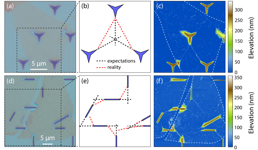
Figures 1-2 have shown that the use of a thin hBN flake over a nano-patterned substrate to regulate the amount of strain in WSe2 may be a better choice to create single WSe2 QEs than using substrate features directly to strain WSe2. However, the positioning of QEs along hBN wrinkles in these samples is random, whether at a kink or in nano-bubbles. The remainder of this paper focuses on ways to create hBN wrinkles so as to control the positioning of QEs. A single wrinkle only provides one in-plane dimension of confinement, similar to semiconductor nanowires. We have considered several ways to extend the confinement provided by wrinkles to two in-plane dimensions. As a first approach, we designed the structures shown in Fig. 4, which are meant to have two propagating wrinkles cross and create a high strain point. Figure 4(a,b,c) show an optical micrograph and an AFM image of sample 3a containing star-triangle structures overlaid by a thin hBN flake. In most cases, wrinkles connect nearest-neighbor ridge structures instead of propagating independently and in the direction of the ridge, i.e., creating a crossing of two wrinkles is not straightforward. Moreover, since the transfer process is manually operated and uses a visco-elastic PDMS stamp, the details of the transfer matter: propagation direction, transfer speed and amount of pressure applied all influence the outcome. In Fig. 4(d,e,f), we show sample 3b containing propagating ridges with varying separation angles. At shallow angles (30 degrees), the ridges do form wrinkles that propagate in the direction of the ridge, however, rather than crossing, the two wrinkles avoid one another, ending up propagating in a roughly parallel path. At larger angles, the wrinkles bind directly between nearest-neighbor ridge ends as seen in Fig. 4(c). Figures. 4(b) and (e) sum up our expected and observed wrinkle propagation direction as black and red dashed lines, respectively. We conclude that creating two independent hBN wrinkles to achieve a wrinkle crossing is not feasible. Other approaches may be better, e.g., a hybrid sample designed such that a single hBN wrinkle crosses a lithographically defined shallow feature to bring additional strain on a single wrinkle.
Several groups have demonstrated that strain activation of QEs extends beyond the use of nanopillars, by using e.g., slotted waveguides Kern et al. (2016); Blauth et al. (2018) or hBN nano-bubbles Shepard et al. (2017). We also exemplify the universality of strain induction of QEs in WSe2 monolayers by using a star-triangle patterned substrate (sample 3a) with a WSe2/hBN heterostructure. The heterostructure is transferred on top of 12 star-triangle shapes: we record bright distinguishable emission centers on every structure with an average of 2.9 bright centers per star-triangle feature and an average of 3.1 emitters per bright center (out of 21 studied). Figure 5 shows results from two star-triangles. The AFM images in Fig. 5(a)(d) show how the heterostructure conforms to the star-triangle shape. Interestingly, we notice a wrinkle pattern on top of each star that resembles a triangle. In both instances, bright emission centers appear at the tip of one branch and from the center of the structure, see PL map in Fig. 5(b)(e). The star-triangle shape is indicated in a yellow dashed line and was inferred from cross referencing the PL-map, AFM scan and optical image of the sample. The associated spectra and filtered are shown in Fig. 5(c)(f). The spectra are reminiscent of those collected from pillars in samples 1 and 2, where the background level is rather pronounced. The bright emission centers recorded at the center of the star-triangle may be coming from the wrinkles that form on top of the stars in the AFM images. However, we speculate that the tightness of the wrinkles along with the complexity on top of the star structures creates a complex strain profile, hence the more crowded spectra. The filtered extracted from the fit are 0.14 and 0.16. This sample shows that working with any structure that produces local strain is likely to create QEs in WSe2 and that the spectral quality of emitters can vary based on transfer process, hBN thickness and morphology.
Conclusion
We have reported the observation of WSe2 quantum emitters that form from strain created along hexagonal boron nitride wrinkles. These emitters have been shown to be frequently isolated from other emitters and background emission. Quantum emitters found along hBN wrinkles typically have a peak-to-background ratio exceeding 90 %, which defines the fraction of a QE intensity over all the collected light in a 3 nm spectral window. Remarkably, an analysis of the unfiltered spectrum shows that on average, bright emission centers associated with QEs along hBN wrinkles contain four times as little residual emission (background and other emitters) compared to emitters formed directly on substrates features such as a nanopillar. We also found that using a capping hBN layer to protect WSe2 QEs from the environment confers the best configuration to suppress spectral wandering and blinking in our study. In particular, we attribute the ideal spectral stability of wrinkle QEs to the fact that hBN wrinkles elevate WSe2 from the SiO2 substrate, while pillar emitters remain in contact with the substrate. Finally, we have studied alternative substrates to control hBN wrinkle propagation and conclude that crossing two wrinkles to create a high-strain point is not feasible. We suggest for a future work that propagating a hBN wrinkle over a perpendicularly defined shallow structure could create a high-strain point along the wrinkle, thereby creating a WSe2 QE with position control. Our combined results – single QE created per site, low surrounding background, and spectral stability – make wrinkle-based WSe2 QEs promising for applications requiring highly pure single-photon sources Lodahl, Mahmoodian, and Stobbe (2015); O’Brien, Furusawa, and Vučković (2009); Gisin et al. (2002); Kimble (2008). Further research that enables the use of the valley properties of WSe2 excitons would bring even more functionality to the source, such as control over photon polarization Mak and Shan (2016).
Author’s contributions
RSD, TAV and GDF designed the experiment and wrote the manuscript. RSD and TAV prepared samples, collected and analyzed data. AM and ANV performed additional measurements on the samples. ZW, KFM and JS helped with sample preparation. All authors reviewed the manuscript.
Data Availability
The data that support the findings of this study are available from the corresponding author upon reasonable request.
acknowledgments
This work was primarily supported by an AFOSR MURI (FA9550-18-1-0480) with partial support from the Cornell Center for Materials Research (CCMR) with funding from the NSF MRSEC program (DMR-1719875), NSF Career (DMR-1553788) and AFOSR FA9550-19-1-0074. We also acknowledge facility use from the CCMR and from the Cornell NanoScale Facility, a member of the National Nanotechnology Coordinated Infrastructure (NNCI), which is supported by the National Science Foundation (NNCI-1542081).
Appendixes
Appendix A Peak-to-background ratio calculation details
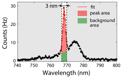
Figure 6 shows the spectrum of wrinkle QE B from sample 2 (see Fig. 2(e)) along with a fit of the QE line. The fitted function is composed of a Lorentzian lineshape plus a wavelength-dependent background as discussed in the main text. The peak area and background are calculated by summing the pixels of the red and green area within a spectral window of 3 nm indicated as a dashed box. In this example, the computed .
References
- O’Brien, Furusawa, and Vučković (2009) J. L. O’Brien, A. Furusawa, and J. Vučković, “Photonic quantum technologies,” Nat. Photonics 3, 687–695 (2009).
- Gisin et al. (2002) N. Gisin, G. Ribordy, W. Tittel, and H. Zbinden, “Quantum cryptography,” Rev. Mod. Phys. 74, 145 (2002).
- Kimble (2008) H. J. Kimble, “The quantum internet,” Nature 453, 1023–1030 (2008).
- Aharonovich, Englund, and Toth (2016) I. Aharonovich, D. Englund, and M. Toth, “Solid-state single-photon emitters,” Nat. Photonics 10, 631 (2016).
- Mak and Shan (2016) K. F. Mak and J. Shan, “Photonics and optoelectronics of 2D semiconductor transition metal dichalcogenides,” Nat. Photonics 10, 216 (2016).
- Schaibley et al. (2016) J. R. Schaibley, H. Yu, G. Clark, P. Rivera, J. S. Ross, K. L. Seyler, W. Yao, and X. Xu, “Valleytronics in 2D materials,” Nat. Rev. Mater. 1, 1–15 (2016).
- Srivastava et al. (2015) A. Srivastava, M. Sidler, A. V. Allain, D. S. Lembke, A. Kis, and A. Imamoğlu, “Optically active quantum dots in monolayer ,” Nat. Nanotech. 10, 491 (2015).
- He et al. (2015) Y.-M. He, G. Clark, J. R. Schaibley, Y. He, M.-C. Chen, Y.-J. Wei, X. Ding, Q. Zhang, W. Yao, X. Xu, C.-Y. Lu, and J.-W. Pan, “Single quantum emitters in monolayer semiconductors,” Nat. Nanotech. 10, 497–502 (2015).
- Koperski et al. (2015) M. Koperski, K. Nogajewski, A. Arora, V. Cherkez, P. Mallet, J.-Y. Veuillen, J. Marcus, P. Kossacki, and M. Potemski, “Single photon emitters in exfoliated structures,” Nat. Nanotech. 10, 503 (2015).
- Chakraborty et al. (2015) C. Chakraborty, L. Kinnischtzke, K. M. Goodfellow, R. Beams, and A. N. Vamivakas, “Voltage-controlled quantum light from an atomically thin semiconductor,” Nat. Nanotech. 10, 507 (2015).
- Chakraborty et al. (2019) C. Chakraborty, N. R. Jungwirth, G. D. Fuchs, and A. N. Vamivakas, “Electrical manipulation of the fine-structure splitting of WSe2 quantum emitters,” Phys. Rev. B 99, 045308 (2019).
- Chakraborty et al. (2017) C. Chakraborty, K. M. Goodfellow, S. Dhara, A. Yoshimura, V. Meunier, and A. N. Vamivakas, “Quantum-confined Stark effect of individual defects in a van der Waals heterostructure,” Nano Letters 17, 2253–2258 (2017).
- Chakraborty et al. (2018) C. Chakraborty, L. Qiu, K. Konthasinghe, A. Mukherjee, S. Dhara, and N. Vamivakas, “3D localized trions in monolayer in a charge tunable van der Waals heterostructure,” Nano Letters 18, 2859–2863 (2018).
- Brotons-Gisbert et al. (2019) M. Brotons-Gisbert, A. Branny, S. Kumar, R. Picard, R. Proux, M. Gray, K. S. Burch, K. Watanabe, T. Taniguchi, and B. D. Gerardot, “Coulomb blockade in an atomically thin quantum dot coupled to a tunable Fermi reservoir,” Nat. Nanotech. 14, 442–446 (2019).
- Branny et al. (2017) A. Branny, S. Kumar, R. Proux, and B. D. Gerardot, “Deterministic strain-induced arrays of quantum emitters in a two-dimensional semiconductor,” Nat. Comm. 8, 1–7 (2017).
- Palacios-Berraquero et al. (2017) C. Palacios-Berraquero, D. M. Kara, A. R.-P. Montblanch, M. Barbone, P. Latawiec, D. Yoon, A. K. Ott, M. Loncar, A. C. Ferrari, and M. Atatüre, “Large-scale quantum-emitter arrays in atomically thin semiconductors,” Nat. Comm. 8, 1–6 (2017).
- Kern et al. (2016) J. Kern, I. Niehues, P. Tonndorf, R. Schmidt, D. Wigger, R. Schneider, T. Stiehm, S. Michaelis de Vasconcellos, D. E. Reiter, T. Kuhn, and R. Bratschitsch, “Nanoscale positioning of single-photon emitters in atomically thin WSe2,” Advanced materials 28, 7101–7105 (2016).
- Shepard et al. (2017) G. D. Shepard, O. A. Ajayi, X. Li, X. Y. Zhu, J. Hone, and S. Strauf, “Nanobubble induced formation of quantum emitters in monolayer semiconductors,” 2D Materials 4, 021019 (2017).
- Zheng et al. (2019) Y. J. Zheng, Y. Chen, Y. L. Huang, P. K. Gogoi, M.-Y. Li, L.-J. Li, P. E. Trevisanutto, Q. Wang, S. J. Pennycook, A. T. S. Wee, and S. Y. Quek, “Point defects and localized excitons in 2D WSe2,” ACS Nano 13, 6050–6059 (2019).
- Cai et al. (2018) T. Cai, J.-H. Kim, Z. Yang, S. Dutta, S. Aghaeimeibodi, and E. Waks, “Radiative enhancement of single quantum emitters in WSe2 monolayers using site-controlled metallic nanopillars,” ACS Photonics 5, 3466–3471 (2018).
- Proscia et al. (2018) N. V. Proscia, Z. Shotan, H. Jayakumar, P. Reddy, C. Cohen, M. Dollar, A. Alkauskas, M. Doherty, C. A. Meriles, and V. M. Menon, “Near-deterministic activation of room-temperature quantum emitters in hexagonal boron nitride,” Optica 5, 1128–1134 (2018).
- Wang et al. (2013) L. Wang, I. Meric, P. Y. Huang, Q. Gao, Y. Gao, H. Tran, T. Taniguchi, K. Watanabe, L. M. Campos, D. A. Muller, J. Guo, P. Kim, J. Hone, K. L. Shepard, and C. R. Dean, “One-dimensional electrical contact to a two-dimensional material,” Science 342, 614–617 (2013).
- Kumar, Kaczmarczyk, and Gerardot (2015) S. Kumar, A. Kaczmarczyk, and B. D. Gerardot, “Strain-induced spatial and spectral isolation of quantum emitters in mono-and bilayer ,” Nano Letters 15, 7567–7573 (2015).
- Darlington et al. (2020) T. P. Darlington, C. Carmesin, M. Florian, E. Yanev, O. Ajayi, J. Ardelean, D. A. Rhodes, A. Ghiotto, A. Krayev, K. Watanabe, T. Taniguchi, J. W. Kysar, A. N. Pasupathy, J. C. Hone, F. Jahnke, N. J. Borys, and P. J. Schuck, “Imaging strain-localized exciton states in nanoscale bubbles in monolayer WSe2 at room temperature,” arXiv:2003.01789 (2020).
- Broome et al. (2013) M. A. Broome, A. Fedrizzi, S. Rahimi-Keshari, J. Dove, S. Aaronson, T. C. Ralph, and A. G. White, “Photonic boson sampling in a tunable circuit,” Science 339, 794–798 (2013).
- Kumar et al. (2016) S. Kumar, M. Brotóns-Gisbert, R. Al-Khuzheyri, A. Branny, G. Ballesteros-Garcia, J. F. Sánchez-Royo, and B. D. Gerardot, “Resonant laser spectroscopy of localized excitons in monolayer ,” Optica 3, 882–886 (2016).
- Lodahl, Mahmoodian, and Stobbe (2015) P. Lodahl, S. Mahmoodian, and S. Stobbe, “Interfacing single photons and single quantum dots with photonic nanostructures,” Rev. Mod. Phys. 87, 347 (2015).
- Tonndorf et al. (2015) P. Tonndorf, R. Schmidt, R. Schneider, J. Kern, M. Buscema, G. A. Steele, A. Castellanos-Gomez, H. S. J. van der Zant, S. M. de Vasconcellos, and R. Bratschitsch, “Single-photon emission from localized excitons in an atomically thin semiconductor,” Optica 2, 347–352 (2015).
- Iff et al. (2017) O. Iff, Y.-M. He, N. Lundt, S. Stoll, V. Baumann, S. Höfling, and C. Schneider, “Substrate engineering for high-quality emission of free and localized excitons from atomic monolayers in hybrid architectures,” Optica 4, 669–673 (2017).
- Santori et al. (2001) C. Santori, M. Pelton, G. Solomon, Y. Dale, and Y. Yamamoto, “Triggered single photons from a quantum dot,” Phys. Rev. Lett. 86, 1502 (2001).
- Linhart et al. (2019) L. Linhart, M. Paur, V. Smejkal, J. Burgdörfer, T. Mueller, and F. Libisch, “Localized intervalley defect excitons as single-photon emitters in WSe2,” Phys. Rev. Lett. 123, 146401 (2019).
- Dang et al. (2020) J. Dang, S. Sun, X. Xie, Y. Yu, K. Peng, C. Qian, S. Wu, F. Song, J. Yang, S. Xiao, L. Yang, Y. Wang, and C. W. . X. X. M. A. Rafiq, “Identifying defect-related quantum emitters in monolayer WSe2,” NPJ 2D Materials and Applications 4, 1–7 (2020).
- Blauth et al. (2018) M. Blauth, M. Jürgensen, G. Vest, O. Hartwig, M. Prechtl, J. Cerne, J. J. Finley, and M. Kaniber, “Coupling single photons from discrete quantum emitters in WSe2 to lithographically defined plasmonic slot waveguides,” Nano Letters 18, 6812–6819 (2018).