Topological quantum switch and controllable quasi 1D wires in antimonene
Abstract
Based on the recently found non-trivial topology of buckled antimonene, we propose the conceptual design of a quantized switch that is protected by topology and a mechanism to create configurable 1D wire channels. We show that the topologically required edge states in this system can be turned on and off by breaking the inversion symmetry (reducing the symmetry from to ), which can be achieved by gating the system. This is shown to create a field-effect quantum switch projected by topology. Secondly we show that by locally gating the system with different polarity in different areas, a soliton-like domain wall is created at their interface, which hosts a protected electronic state, in which transport could be accessed by gated doping.
Introduction:
Mono-layer antimony (antimonene) in the honeycomb lattice (-Sb) is emerging rapidly as a 2D system exhibiting various interesting physical phenomena. RecentlyRadha and Lambrecht (2019) we showed that this system in its flat state (which is a nodal line semimetal) is the first example of planar goniopolarity: i.e. the transport carrier is hole- or electron-like depending on in-plane direction. We also showed that the much sought after Dirac cone annihilation physics can in principle be achieved in this system by controlling the in-plane tensile strain. Two topologial transitions occur under increasing buckling (decreasing in plane tensile strain) at which pairs of Dirac cones (of opposite winding number) protected by the crystal symmetry axes annihilate when band inversion occurs between bands beloging to different irreducible representations. In another paperRadha and Lambrecht (2020) we showed that the fully buckled equilibrium structure of the free standing monolayer is a Higher Order Topological Insulator (HOTI) with protected corner states. Chiel et al. Chiel et al. (2019) showed that the buckled form could host mechanical edge modes leading to strain solitons. It is particularly promising that these need not be confined to theoretical predictions because several experimental routes to achieve monolayers of -Sb have already been reported, including mechanical exfoliation and epitaxial growth.Ares et al. (2018); Ji et al. (2016)
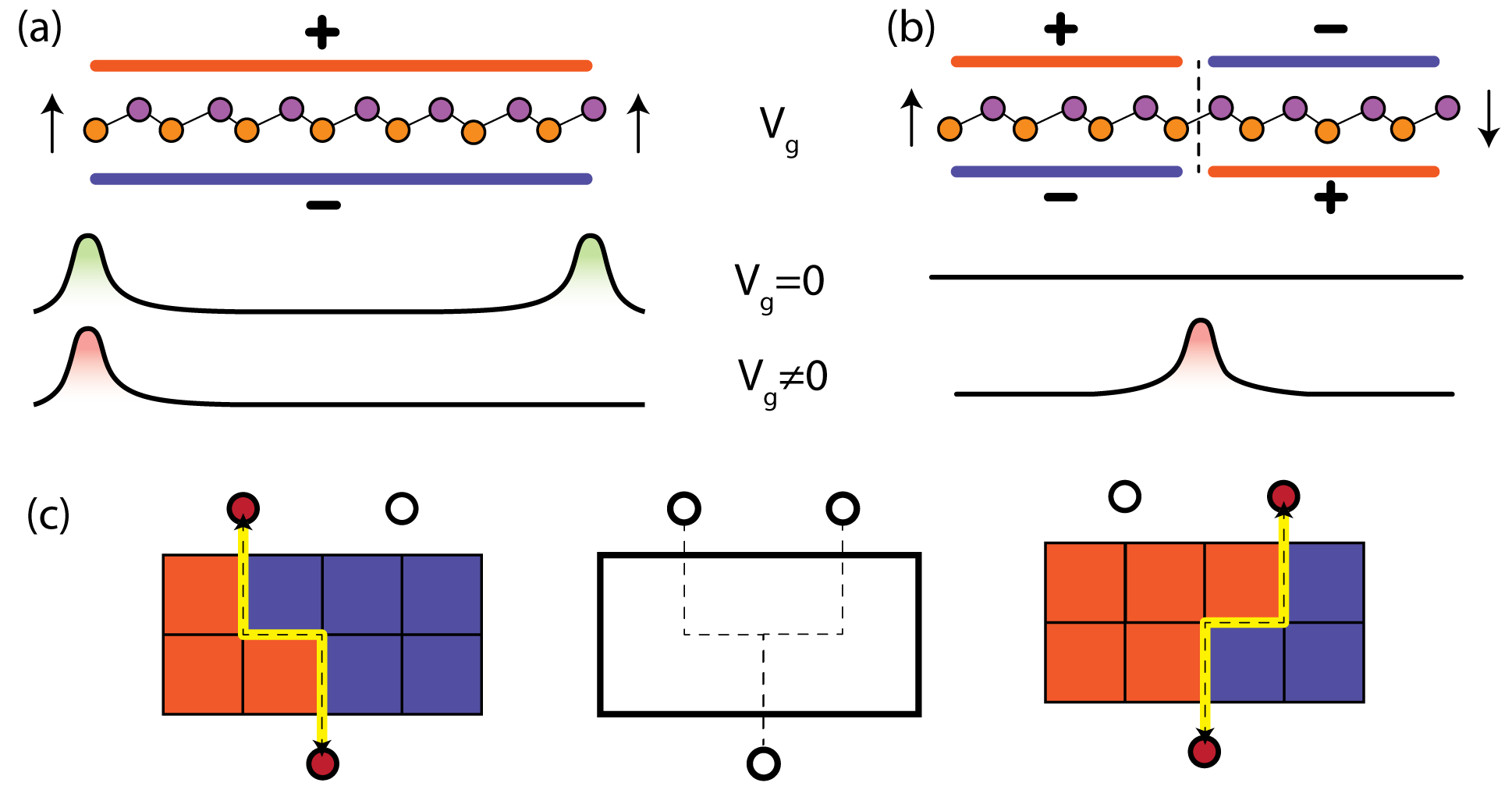
Field effect transistors (FET) are the key elements in modern electronics and function by turning on and off the conductivity through a channel between source and drain by means of a gate. Typically, the channel is a 2D electron gas between two semiconductors and the gate voltage is applied through an insulating layer, such as an oxide in a MOSFET, which thereby controls the carrier concentration in the 2D gas. An important quantity is the ratio between on and off state resistance. Here we propose a switch based on turning off the conduction in topological edge states of a 2D topological crystal insulator by means of an electric field gate. In the 2D Sb system under consideration, the conducting edge states are topologically protected by inversion symmetry and an electric field breaks the inversion symmetry thereby turning the conducting channel off in an abrupt way. Furthermore the conductance itself can be in the ballistic quantized regime. This is illustrated in Figure 1 (left).
A somewhat related but not identical idea for a topology based switching device was proposed by Liu et al. Liu et al. (2014). However that device is based on breaking the mirror plane symmetry, which protects a topological state, by means of an electric field in the 3D material SnTe. Strong effects on magnetotransport due to mirror symmetry breaking were also reported by Wei et al. Wei et al. (2018).
.
A second intriguing idea in advanced electronics is that of reconfigurable circuits. Cheng et al. Cheng et al. (2011, 2013); Bi et al. (2010) demonstrated this idea by creating a conducting local 2D electron gas at the LAO/STO (LaAlO3/SrTiO3) interface induced by removing surface adsorbed OH groups using a scanning tunneling microscope tip along selected lines drawn on the surface of LAO a few layers above the LAO/STO interface. Here we propose a different mechanism for creating reconfigurable quasi 1D semi-conducting channels in the monolayer Sb system. Furthermore the conductance in this 1D system could show quantized conductance in the low-temperature ballistic regime.Imryt (1987) This is also based on breaking the inversion symmetry. But instead of breaking it in the entire system, we show that by locally breaking inversion with opposite polarity one can form domain walls hosting localized 1D dispersing states in the gap which can become semi-conducting channels for electron or holes. Unlike the drawing mechanism used in the LAO/STO system, which requires nanoscale scanning probe type manipulations, the process to reconfigure the path in our proposed scheme is much simpler. First, it is a low energy process as one needs a very small amount of bias to open and close the channel because its existence is based on topology. Second it would only involve applying bias voltages to a static configuration of localized pixelated gates without the need for mechanical motion. A schematic illustration of this device is shown in Figure 1 (right)
The main idea behind both types of devices presented here is based on applying an electric field normal to the layers which breaks the inversion symmetry between the two sublattices because of the alread present buckling which exposes each sublattice to a different potential in the presence of an electric field. The use of an electric field normal to the layers of a 2D system to tune the electronic structure has been considered before, in particular for flat monolayer Sb.Hsu et al. (2016) However, in that case the electric field’s role is to break the horizontal mirror plane rather than the inversion symmetry. The topological edge states in that regime are different and result from the spin-orbit coupling.
Symmetry and topology:
In monolayer honeycomb group-V systems, unlike in graphene, the atomic -orbital derived bands are disentangled from the -orbitals.Radha and Lambrecht (2019) In the completely flat limit, interaction between and is absent because of mirror symmetry. Buckling breaks the mirror symmetry and becomes a tuning parameter for the interaction and after a critical angle ( for Sb) or equivalently reduction of tensile in-plane strain, the system gaps up and attains the lowest energy stable structure that has been synthesizedJi et al. (2016). In this structure, all three orbitals are hybridized and determine the low-energy physics near the gap, by forming a set of bonding and antibonding combinations in the valence and conduction band respectively. As described in Ref. Radha and Lambrecht, 2020 the valence band manifold has bond-centered Wannier functions obeying symmetry. This places the system in the “obstructed atomic limit” (OAL) as defined by Bradlyn et al. Bradlyn et al. (2017); Cano et al. (2018) which has non-trivial crystalline topological (TCI) properties, leading to weakly protected edge-states as well as corner states. In Ref. Radha and Lambrecht, 2020 we showed the system can be mapped to the bond-alternating honeycomb or Kekulé lattice, which can be viewed as a 2D generalization of the iconical Su-Schrieffer-Heeger (SSH) model whose alternating weak and strong bonds are well known to lead to protected end states when the unit cell is chosen so that the strong bonds are broken at the ends of a finite chain. The group has 3D inversion as well as symmetry operations and it is the inversion symmetry which protects the edge and corner states.Benalcazar et al. (2019); Schindler et al. (2019); Radha and Lambrecht (2020) This inversion is directly connected with the identical Sb atoms in this bipartite system, which leads to mid-gap 1D edge bands and corner states of 0D symmetry preserving flakes.
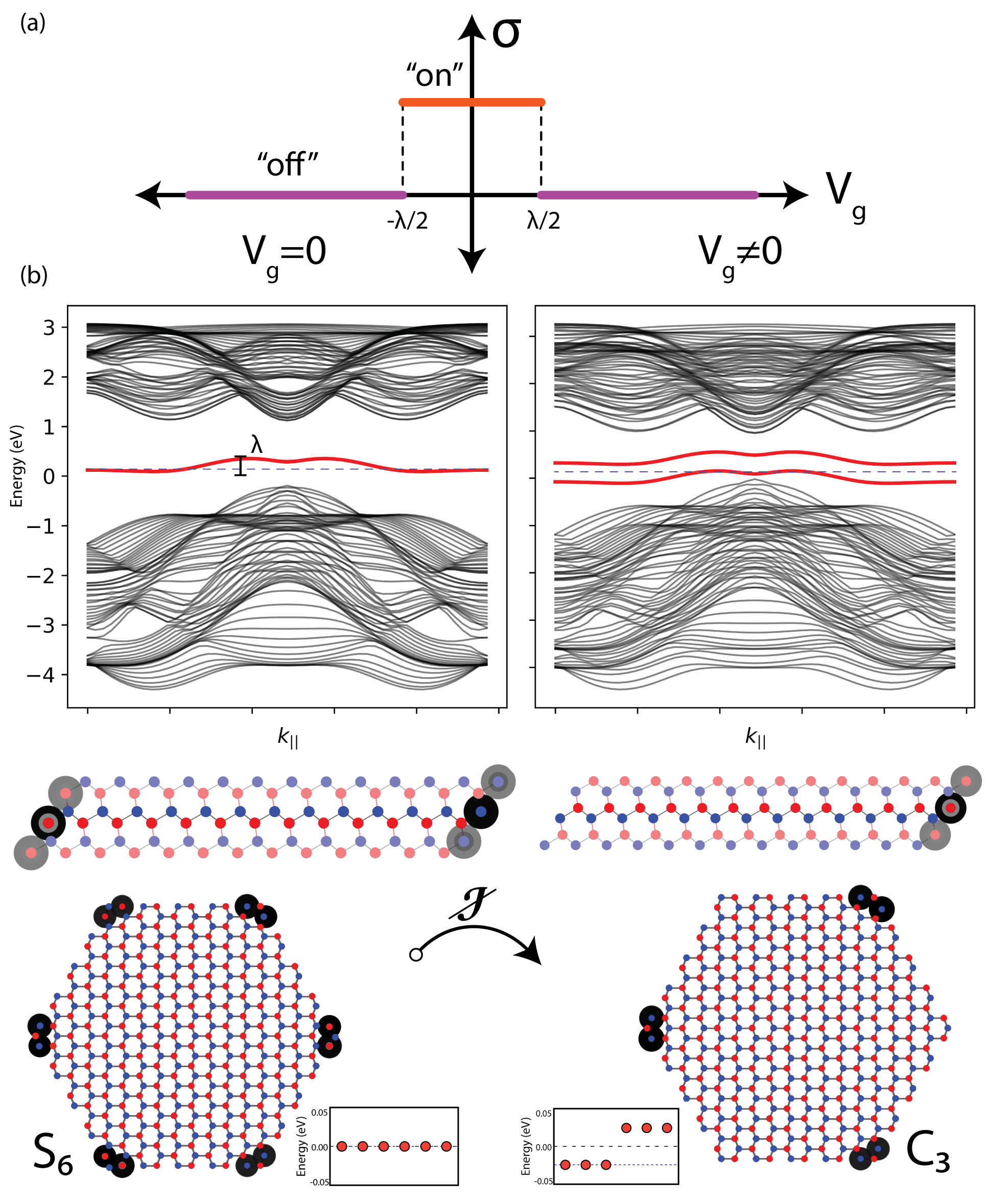
Unlike for a flat honeycomb lattice, because of buckling, one can easily break this sub-lattice (inversion) symmetry by an applied electric field (or gating) in the direction perpendicular to the layers, thereby creating a modulated on-site potential. This is obvious from Figure 1. This then leads to a point group as the reduced symmetry. As a result the edge states gap up and hence the fractionalized electrons previously spread over the two identical edges will now reside on the one edge (corner) with the lower energy. This, in principle, leads from partially filled edge (corner) states on both edges to a completely filled and empty edge (corner) state on opposite sides and hence a metal-insulator transition in the case of dispersing edge states or a switch in which half of the corner states switch from half occupied to fully occupied and the other ones to empty as detailed next.
.
Topological switch:
At low temperature, graphene is known to have quantized low bias conductance in 1D armchair (zigzag) edge modes given byPeres et al. (2006) () with the transmission coefficients to the leads, whereby the conductance occurs in steps but which are not exact multiples of the quantum of conductance. In this nanoscale ballistic transport regime, the conductance is determined by the number of 1D transverse modes contributing to the transport.Imryt (1987) In the present case of a 1D Sb nanoribbon and for zero bias normal to the plane of the ribbon, we have two zero energy edge modes (one for each edge) with half occupation for each spin channel, therefore giving conductance, when the Fermi level lies within this band. In contrast to graphene, where the edge bands connect the host valence and conduction bands, the large gap in the 2D Sb host system ( 3eV) implies a huge barrier before carriers can access the high/low lying 2D host bands in the ribbon giving us zero conductance for any Fermi level location in the gap outside the range set by the 1D dispersion of the edge bands. Note that the dispersive nature of the 1D edge bands and their bandwidth stem from the next nearest neighbor interaction along the parallel direction and are hence small (of order 0.3 eV). Breaking the inversion symmetry between the sublattices by a gate voltage, as already described in the previous section, now opens a gap between the edge bands as soon as the splitting becomes larger than the 1D edge band dispersion. Assuming that the gate voltage changes the on-site potentials on the two sub-lattices by and thus opens a splitting between the energy centers of the two edge bands and a dispersion in the edge modes of width , a gap between the two edge bands occurs when and one enters the insulating limit with zero conductance. Because is small compared to the gap of the 2D system, only a small gate voltage will be required to switch the device from its “on” (conducting) to its “off” or insulating state.
There are three major advantages to device of this type compared to traditional switches: (i) this switch has topological protection as the on state is protected from perturbations including defects in the lattice because of topological non-triviality (as shown in Radha and Lambrecht (2020)); (ii) unlike traditional switches, we have quantized binary states; and finally (iii) the barrier to turn off the switch requires only low power with a value set by the dispersion of the edge modes.
Another possible device that uses the inversion symmetry as switch is to use the same mechanism in the corresponding finite size symmetric hexagonal flakes of the system. With inversion symmetry preserving the , one is guaranteed (spinless) charge fractionalization of in each sector. But as soon as one reduces the symmetry to , the edge modes can interact and open a gap. This leads to the charges being transferred to the respective previously inversion symmetric point. (Including spin the charge trasfer occurs for each spin so becomes .) Thus at zero bias voltage, where inversion symmetry is preserved, one has no potential difference between each sectors while a inversion breaking non-zero bias potential difference between symmetric inversion points as shown in Figure 2(c).
1D Quantum wires:
We now look at selectively breaking inversion symmetry in the system with opposite polarity which we will show leads to a domain boundary localized state in the gap. To gain qualitative insight, note that breaking inversion by biasing the system essentially acts like adding a mass gap of to the 1D SSH system. This breaks the chiral/inversion symmetry (in the 1D case) which can be easily seen in the finite 1D chain with one end being A site and the other end being B site. Thus the previously degenerate edge modes trivially gap with the occupied state being at the low energy side. The same physics holds here with one edge being occupied by the low potential part of the inversion broken sub-lattice and other side being empty when an inversion breaking bias is applied.
.
For creating a 1D quantum wire, we split the device into two regions, where in one region we apply a bias voltage of and in the other . This has the effect of creating alternating onsite terms on one side and the opposite onsite terms on the other side with the junction between them having a domain wall of two . To understand the energetics of this system, we start by looking at the same effect in a simpler 1D SSH, which is nothing but the 1D projection of the buckled Sb 2D system. The SSH Hamiltonian can be written as
| (1) |
where creates (annihilates) an electron in unit cell on sublattice site and is the Heaviside step function. The first terms is the usual SSH Hamiltonian with controlling the hopping anisotropy. For , we are at the critical point between the trivial/non-trivial regimes of the SSH model and the system would be metallic with zero gap. However, the effect we are concerned with here would still be valid because it depends on the second term. We just want a gap to more clearly see the edge states but whether the SSH gap is of the trivial or non-trivial type is irrelevant for the following discussion. The second term here adds a mass gap of for and for . It is easy to see that this system has inversion w.r.t. origin, the sites to the left and right of origin (A and B) gain the same value of to their on-site term.
.
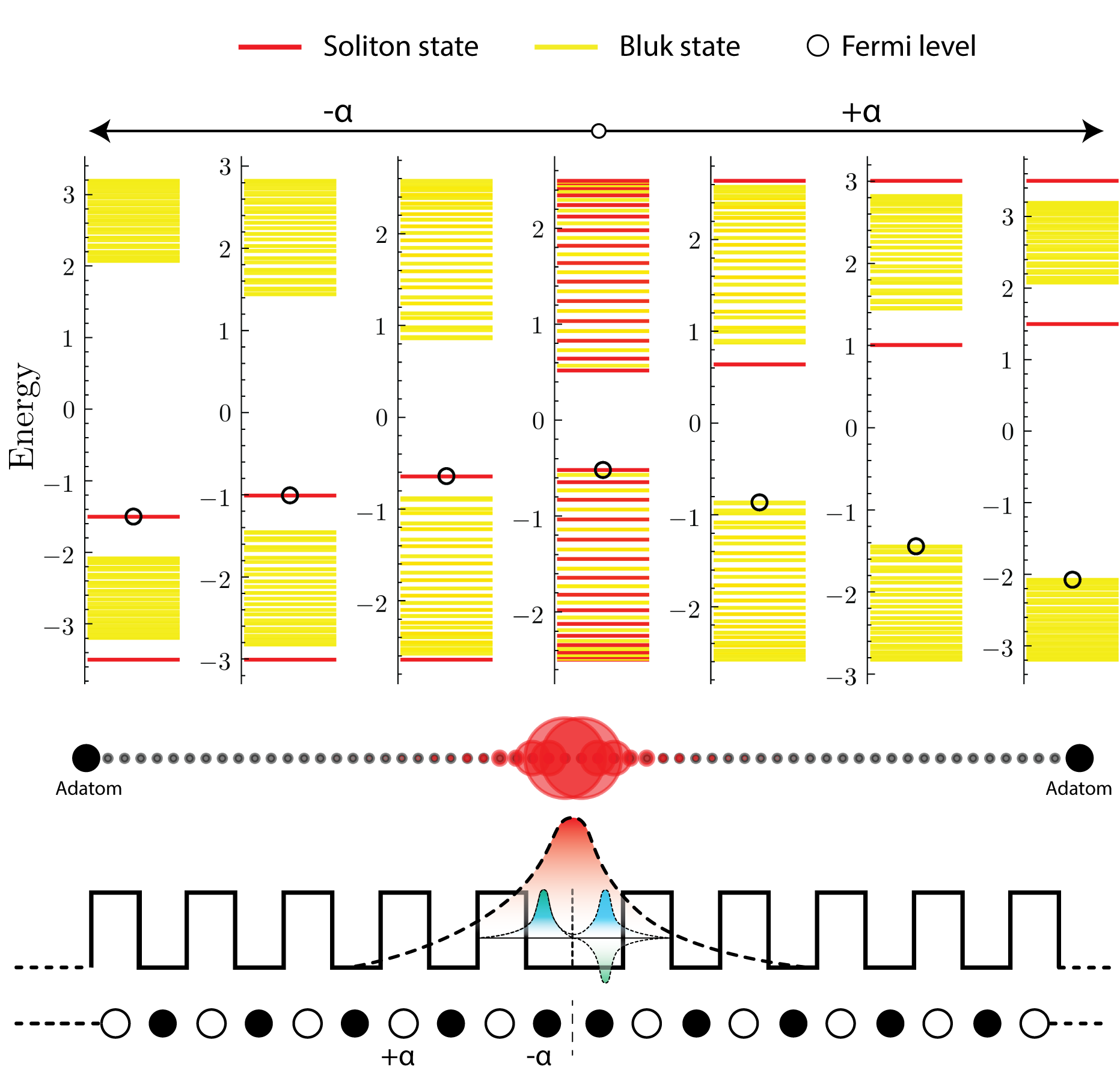
Figure 3 shows the eigenvalue spectrum of the system. The states colored red are the ones localized at the origin where the switch occurs between the two polarities. Since the system has lost its periodicity because of the step function, we treat the system as a large but finite number of sites. Whether it is trivial or not depends on the sign of . We consider a system with , so that there is indeed a gap as in the SSH. In the non-trivial limit we would have an edge state which is not essential for the following discussion and hence is avoided by adding an adatom to the edges as shown in Figure 3. For the effect we consider, it is not important whether the SSH is in the trivial or non-trivial regime as long as there is a gap. Indeed the effect is related to the potential shifts on the atoms rather than on the alternation of strong and weak bonds. Alternatively, we may also envision a periodic Kronig-Penney (KP) type model with alternating wells and barriers. Starting from a finite chain, what the gate voltage does is to flip the wells into barriers in the right half of the system, which creates a well of double width at the center as two atoms with on-site shift and become adjacent at the boundary between the two regions. For the opposite gate voltage, occurs at both center atoms, or in the KP model, a barrier of double width occurs.
For (shown in middle of the top plot), one can see that the spectrum is gapped because of the interaction anisotropy from but the energy states are all having comparable contribution at the origin. In other words, the states are extended and not localized at the domain boundary. Next, applying a negative bias to the atoms next to the origin, as illustrated at the bottom, we see that states localized at the origin (indicated in red) form below and above the occupied bands. They split farther and farther apart from the continuum of levels as the magnitude of the bias is increased.
For as in the case of SSH, we have bonding valence and anti-bonding conduction bands in the lattice with respect to the strong bond. Within the valence band, the weak bonds will form the most bonding combination of the bond-centered Wannier orbitals (same sign on each site) at the bottom of the valence band and the most antibonding arrangement, (alternating signs) at the top of the band. But with the on-site shift, at the domain boundary we create a pair of local bonding and anti-bonding states from the domain boundary adjacent atoms. Thus a state with even stronger bonding character forms below and another one with more antibonding character above the VBM. In the KP model, one may think of the lowest state in each well as corresponding to a strong bond of the SSH model and these bond orbitals are now weakly coupled by tunneling through the barriers and forming a band. In this context, one might reason that the center well being wider will have a lower level and hence when it interacts with the other wells, a new level will appear below the band. But there will now also be a second antisymmetric band in the central well of double width and this one will occur slightly above the band but well below the CBM formed by broadening the antisymmetric states of the narrow wells into a band. The electron count does not change, so this level becomes the highest occupied level of the system and is fully occupied. Thus, one can see that we have essentially created a potential domain wall hosting a localized state at the origin, as shown in the bottom part of Figure 3. If the system is slightly doped p-type, say by removing one electron from the whole system, the split-off top level localized at the center will become partially filled, or in other words, a hole becomes preferentially trapped at this site.
For opposite polarity, where the two central atoms experience an upward potential shift or a barrier, we can see in the right panels of energy levels, that now states localized on the origin appear above and below the conduction band. In the KP model one may think of this bound state in the gap as resulting from having a weaker tunneling trough the double well at the center. The highest occupied band stays at the top of the valence band but a bound state localized near the domain wall now appears below the conduction band. So, for slight n-type doping the electron will become localized at the boundary.
We may call this domain wall boundary localized state a soliton state. In fact, the boundary could be moved in principle by shifting the region where positive and negative bias is applied, which would move the localized state around like a solitary wave. Note, however, that it does not originate from having two strong bonds or two weak bonds next to each other as in the SSH soliton like states but rather by having two adjacent atoms with downward or upward potential (or mass shift).
Another interesting perspective for the occurrence of this state can be deduced from topology. Breaking chiral symmetry breaks the notion of topological protection for the system, but still guarantees one localized occupied and one unoccupied edge mode (as long as SSH non triviality is satisfied)Mong and Shivamoggi (2011). As mentioned before, we essentially have created two copies of non-chiral SSH with one being the mirror symmetric reflection of the other (Figure 3 lowest panel). Thus, at the origin, the ends of these two chains meet which then topologically guarantees us a localized state. The left system consists of a lattice with while right and thus there is a domain boundary between the two ionic lattices creating a protected bound state.
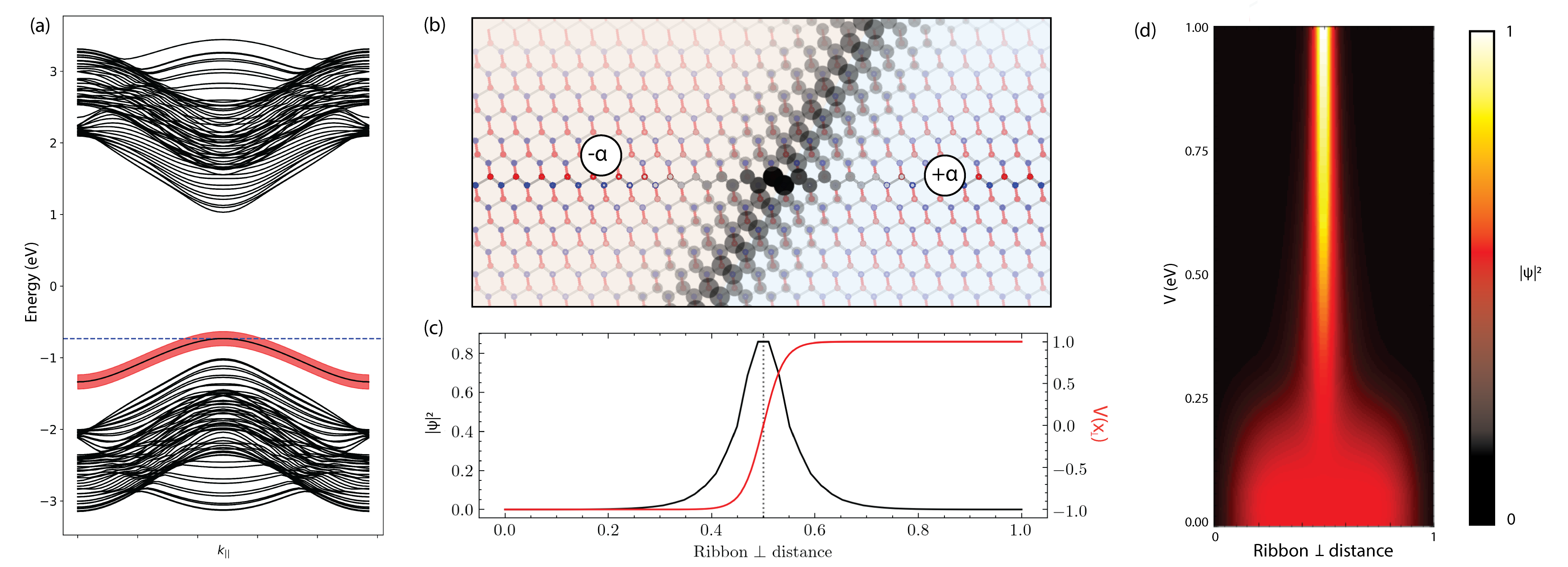
Now moving on to our actual system, we can follow the same procedure to create this domain wall state. But since we have the added dimension , we have a dispersive band at the 1 dimensional domain wall. To simulate a realistic device, we use as shown in Figure 4(c). This essentially ensures that the domain wall is smooth and the smoothness factor is controlled by .Figure 4(a)shows the band structure of this system (for eV). Again, as in the case of SSH, we have added adatoms at the edges of the nanoribbon to remove the outer edge modes. Alternatively, one could use two semi-infinite systems and use a Green’s function technique. Marked in red is the localized domain wall band and its localization is plotted as by the gray scale in Figure 4(b). To numerically check the localization we also look at the which is exponentially localized normal to the domain boundary as shown by the applied potential profile. We also show the degree of localization as function of applied gate voltage in Figure 4(d). Clearly the higher the gate voltage, the narrower the soliton like bound state becomes. Strictly speaking what we mean by gate voltage here is the applied on-site terms on the Sb atoms. How these are related to an actual applied voltage would depend on the technical implementation of the device and the screening or self-consistent potential in the Sb layer. Modeling that in detail is beyond the scope of this qualitative paper which focuses on the concept.
These domain wall states remain occupied/unoccupied and become the highest valence/ lowest conduction bands depending on the sign of just like in the SSH toy model. Thus by electron or hole doping the system (possibly by global gating), one could achieve localized conduction because electrons or holes would thermalize to these domain boundary bound states. Interestingly, since the polarity of the channel dependents on the sign of applied voltage, one can turn a hole doped system conducting and insulating along this channel by simple reversing the global gate polarity.
Although we have here discussed the principle of the creation of a 1D wire only, it doesn’t take much imagination to see that one could apply such opposite voltages in patches creating 1D wires at their boundaries. By creating a pixelated gate on top and below the Sb layer, one could imagine just changing the pattern where the voltages are applied and hence where the wires are created by which pixels are addressed. This is in principle a design for a reconfigurable network or circuit of connecting wires as shown in Figure 1(c). As mentioned above, this localization is guaranteed by topology and thus defects/perturbations in the bulk part away from the domain wall would not interfere with this localization, hence creating robust 1D quantum channels. In order to make the 1D wires at the boundaries conducting the system needs to be doped in just the right way that free carriers, holes or electrons will tend to be confined to the 1D localized domain wall states. This doping itself can conceivably also be realized by a global gating of the system rather than by adding chemical dopant atoms, whereby the overall carrier density in the system would also be controllable. We emphasize that domain walls of this type can be made along several directions in the 2D Sb. Their origin depends on breaking the inversion symmetry and is thus not confined to specific edges, such as zigzag or arm-chair edges at which the domains meet.
Summary:
In this paper we have described two device concepts related to the inversion symmetry breaking in monolayer Sb. Since the inversion symmetry leads to topologically protected edge states, breaking inversion does not remove the edge states but can be used to move the edge states in energy in a controlled way and hence their electron occupation can be controlled. Because of the buckled nature of monolayer honeycomb Sb, this symmetry breaking can be simply created by a gate voltage normal to the layer. This leads to the possibility of creating a switch between a topologically protected metallic edge state to an insulating state protected by the large gap of the host 2D system. Furthermore in the low temperature ballistic limit, the conductance in this 1D edge state would be quantized to a value of apart from a transmission coefficient to the leads connecting to the system. The step-like conductivity switch would be abrupt and the off state is protected by a large gap of these edge states toward the 2D band edges. The bias required for switching the off-state is determined by the band width of the dispersing edge band which follows from second nearest neighbor interactions only and is very small compared to the gap protecting the off state.
Secondly, applying the symmetry breaking of opposite polarity in patches, we have shown that at their interface, a 1D quantum conducting wire state could be created because of the formation of a domain wall localized band. This process can in principle be used to create reconfigurable conducting networks.
Acknowledgements -
We thank Xuan Gao, Shulei Zhang, Arvind Shankar for useful discussions. This work was supported by the U.S. Department of Energy-Basic Energy Sciences under grant No. DE-SC0008933. The calculations made use of the High Performance Computing Resource in the Core Facility for Advanced Research Computing at Case Western Reserve University.
References
- Radha and Lambrecht (2019) S. K. Radha and W. R. L. Lambrecht, “Topological band structure transitions in honeycomb antimonene as function of buckling,” (2019), arXiv:1912.03755 [cond-mat.mtrl-sci] .
- Radha and Lambrecht (2020) S. K. Radha and W. R. L. Lambrecht, “Buckled honeycomb group-– symmetric higher order topological insulators,” (2020), arXiv:2003.12656 [cond-mat.mtrl-sci] .
- Chiel et al. (2019) J. Chiel, H. Mathur, and O. Narayan, “Symmetry breaking, strain solitons and mechanical edge modes in monolayer antimony,” (2019), arXiv:1912.05791 [cond-mat.mes-hall] .
- Ares et al. (2018) P. Ares, J. J. Palacios, G. Abellán, J. Gómez-Herrero, and F. Zamora, Advanced Materials 30, 1703771 (2018).
- Ji et al. (2016) J. Ji, X. Song, J. Liu, Z. Yan, C. Huo, S. Zhang, M. Su, L. Liao, W. Wang, Z. Ni, Y. Hao, and H. Zeng, Nature Communications 7, 13352 (2016).
- Liu et al. (2014) J. Liu, T. H. Hsieh, P. Wei, W. Duan, J. Moodera, and L. Fu, Nature Materials 13, 178 (2014).
- Wei et al. (2018) F. Wei, C.-W. Liu, D. Li, C.-Y. Wang, H.-R. Zhang, J.-R. Sun, X. P. A. Gao, S. Ma, and Z. Zhang, Phys. Rev. B 98, 161301 (2018).
- Cheng et al. (2011) G. Cheng, P. F. Siles, F. Bi, C. Cen, D. F. Bogorin, C. W. Bark, C. M. Folkman, J.-W. Park, C.-B. Eom, G. Medeiros-Ribeiro, and J. Levy, Nature Nanotechnology 6, 343 (2011).
- Cheng et al. (2013) G. Cheng, J. P. Veazey, P. Irvin, C. Cen, D. F. Bogorin, F. Bi, M. Huang, S. Lu, C.-W. Bark, S. Ryu, K.-H. Cho, C.-B. Eom, and J. Levy, Phys. Rev. X 3, 011021 (2013).
- Bi et al. (2010) F. Bi, D. F. Bogorin, C. Cen, C. W. Bark, J.-W. Park, C.-B. Eom, and J. Levy, Applied Physics Letters 97, 173110 (2010), https://doi.org/10.1063/1.3506509 .
- Imryt (1987) Y. Imryt, Philosophical Magazine B 56, 969 (1987), https://doi.org/10.1080/13642818708215333 .
- Hsu et al. (2016) C.-H. Hsu, Z.-Q. Huang, C. P. Crisostomo, L.-Z. Yao, F.-C. Chuang, Y.-T. Liu, B. Wang, C.-H. Hsu, C.-C. Lee, H. Lin, and A. Bansil, Scientific Reports 6, 18993 (2016).
- Bradlyn et al. (2017) B. Bradlyn, L. Elcoro, J. Cano, M. G. Vergniory, Z. Wang, C. Felser, M. I. Aroyo, and B. A. Bernevig, Nature 547, 298 (2017).
- Cano et al. (2018) J. Cano, B. Bradlyn, Z. Wang, L. Elcoro, M. G. Vergniory, C. Felser, M. I. Aroyo, and B. A. Bernevig, Phys. Rev. B 97, 035139 (2018).
- Benalcazar et al. (2019) W. A. Benalcazar, T. Li, and T. L. Hughes, Phys. Rev. B 99, 245151 (2019).
- Schindler et al. (2019) F. Schindler, M. Brzezińska, W. A. Benalcazar, M. Iraola, A. Bouhon, S. S. Tsirkin, M. G. Vergniory, and T. Neupert, Phys. Rev. Research 1, 033074 (2019).
- Peres et al. (2006) N. M. R. Peres, A. H. Castro Neto, and F. Guinea, Phys. Rev. B 73, 195411 (2006).
- Mong and Shivamoggi (2011) R. S. K. Mong and V. Shivamoggi, Phys. Rev. B 83, 125109 (2011).